Platinum contacts for 9-atom-wide armchair graphene nanoribbons
Abstract
Creating a good contact between electrodes and graphene nanoribbons (GNRs) has been a longstanding challenge in searching for the next GNR-based nanoelectronics. This quest requires the controlled fabrication of sub-20 nm metallic gaps, a clean GNR transfer minimizing damage and organic contamination during the device fabrication, as well as work function matching to minimize the contact resistance. Here, we transfer 9-atom-wide armchair-edged GNRs (9-AGNRs) grown on Au(111)/mica substrates to pre-patterned platinum electrodes, yielding polymer-free 9-AGNR field-effect transistor devices. Our devices have a resistance in the range of to in the low-bias regime, which is 2 to 4 orders of magnitude lower than previous reports. Density functional theory (DFT) calculations combined with the non-equilibrium Green’s function method (NEGF) explain the observed p-type electrical characteristics and further demonstrate that platinum gives strong coupling and higher transmission in comparison to other materials such as graphene.
Atomically precise (GNRs) are a family of graphene-based quantum materials which have been predicted to host exotic physical properties and potential electronic applications [1]. Depending on their sizes and terminations, they can manifest magnetically ordered edges [2, 3, 4], tunable band-gaps [5, 6, 7] or high-charge mobility [8]. Properties such as bandgap tunability, topological properities as well as edge magnetism [9, 10, 11] and others are intrinsic to GNRs and only appear when atomic precision in the synthesis is achieved. To translate tehse properties into devices, transfer of the ribbons to an appropriate substrate and create a good electrical contact between the GNRs and the electrodes.
Two main contact approaches have been investigated so far in the literature. One is achieved by the direct deposition of electrodes on top of GNRs with lithographic tools [12, 13, 14, 15, 16]. GNR devices fabricated with this top-contact approach show high, non-Ohmic contacts, and in some cases, the current is limited by the contact resistance [12, 13, 15]. This indicates a poor contact of the GNRs with the possible presence of a large Schottky barrier. Additionally, these top-contact GNR devices can suffer from resist contamination and heating during metal evaporation in the lithography process. This is particularly destructive for the GNRs with reactive edges, such as spin-polarized edges and topologically protected edgestates [17, 11, 18].
Another approach for contacting GNRs is by transferring GNRs onto pre-patterned electrodes. For GNRs grown on Au-mica substrates, a polymer-free transfer of 9-AGNRS has been optimized and used in previous reports of Refs. 14, 19 and Ref. 20 with Pd and graphene electrodes, respectively. However, in the case of Pd nanogaps, large Schottky barriers limited the transport through these devices. Likewise, graphene electrodes did not solve the issue of contact resistance and introduced more uncertainties related to the fabrication, i.e., not well-defined gap sizes and lithography-related PMMA residues on the electrodes, the latter being a known concern for graphene devices [21].
In this letter, we study 9-AGNRs junctions with pre-patterned Pt electrodes forming nanogap ranging from 20 to 100 nm in width and 1 m in length. We transfer the 9-AGNRs after the nanogap fabrication and show GNR devices with low-bias (200 mV) Ohmic resistance in the range of to , orders of magnitude lower than the previous reports [12, 13, 14, 15, 20]. Approximately device yield and low resistance are realized as a result of a cleaner device fabrication process compared to the previous top-contact approach, where GNRs are subjected to polymer contamination and high process temperatures. With the field effect transistor geometry, we further demonstrate the high transmission in the Pt-GNR-Pt junctions with p-type transport properties, concluded from gate-dependent measurements. These observations are rationalized by density functional theory and non-equilibrium Green’s function formalism (DFT+NEGF) calculations, estabilishing platinum as an excellent material for contacting 9-AGNRs.
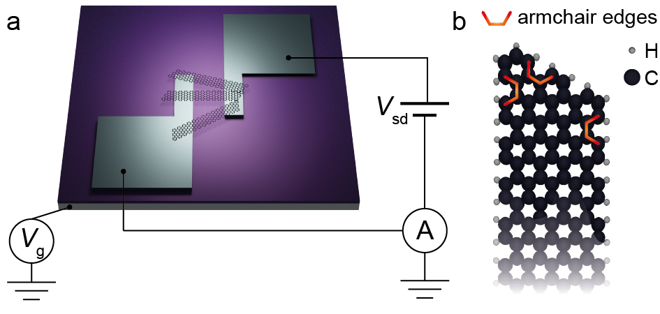
We employ a field-effect transistor geometry to electrically characterize 9-AGNRs in a vacuum probe station. A schematic device lay-out is illustrated in Fig. 1a. With this geometry we measure the current-voltage (IV) characteristics of 9-AGNRs as well as their gate dependence (). The GNRs are transferred onto pre-patterned Pt gaps on a SiO2/Si substrate, where the Si wafer is used as a global back-gate electrode. The 9-AGNRs form transport channels by bridging the pre-patterned lithographically defined Pt nanogaps. The atomic structure of 9-AGNRs is also shown in Fig. 1b, where the four sides of the GNRs are armchair-terminated.
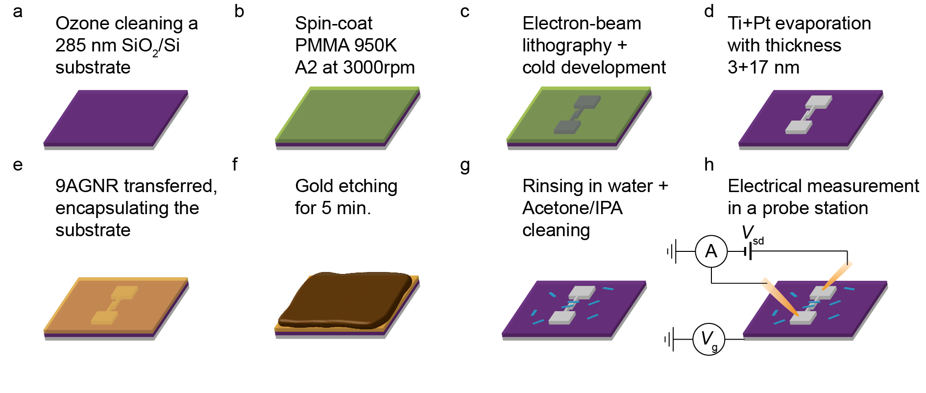
To form a clean 9-AGNR-electrode interface, we pattern Pt electrodes prior to introducing the GNRs, thus avoiding organic contamination of the junction. The device fabrication steps are shown in Fig. 2. We use a SiO2/Si substrate with a thermal oxide thickness of 285 nm. The substrates are first cleaned with acetone and isopropyl alcohol (IPA) for 5 minutes each to remove organic residues on the surface. Subsequently, the substrate is cleaned with an oxygen plasma at a power of 300 W for 3 minutes. After the cleaning, the substrate is spin-coated with PMMA 950K A2 (MicroChem) at 3000 rpm and baked at 180 ∘C for 3 min on a hot plate. This gives a resist thickness of about 80 nm.
The nanogaps with various widths (20-100 nm by design) are patterned by EBPG5000+ (Raith) with an acceleration voltage of 100 kV. To form well-defined nanogaps, a high dose at 2100 is chosen together with a cold development technique. The nanogap structure is developed in IPA:MIBK (3:1) at a temperature of -20∘C for 3 min. Afterwards, the electrodes are made by electron-beam evaporation of 3 nm of Ti at a rate of 0.5 Å/s and 17 nm of Pt at a rate of 1 nm/s, followed by a lift-off process in hot acetone at 50 ∘C. With this thin PMMA resist layer and the cold development method, we achieve Pt nanogap as small as 20 nm with an aspect ratio of more than 100. This allows the possibility to measure end-to-end connected GNRs as they are in the length of few tens of nanometers (see Fig. S1a for a STM image of 9-AGNRs on Au(111)). Moreover, the large aspect ratio provides a high device yield as several 9-AGNRs can be connected in the same junction. Similar nanogaps with large aspect ratio can also be achieved with other methods but require a more elaborated technique such as a chromium oxide mask [22].
To transfer the 9-AGNRs onto the pre-patterned substrate, we follow the polymer-free transfer process described elsewhere [23, 15, 24]. In short, an Au film containing 9-AGNRs delaminates itself from its mica substrate when placed onto an aqueous HCl solution (Fig. 2e). Afterwards, a pre-patterned substrate is used to pull out the free-standing Au film from the diluted HCl solution. To remove the Au film from the 9-AGNRs, the substrate with Au film is covered with a gold etchant for 5 min., as shown in Fig. 2f, and subsequently rinsed with deionized water and cleaned with acetone and IPA. This transfer process preserves the 9-AGNR quality as no peak shift in the Raman spectra of 9-AGNRs was observed, before and after the transfer (Fig. S1b). Afterwards, the sample is mounted in a vacuum probe station at room temperature for electrical characterization.
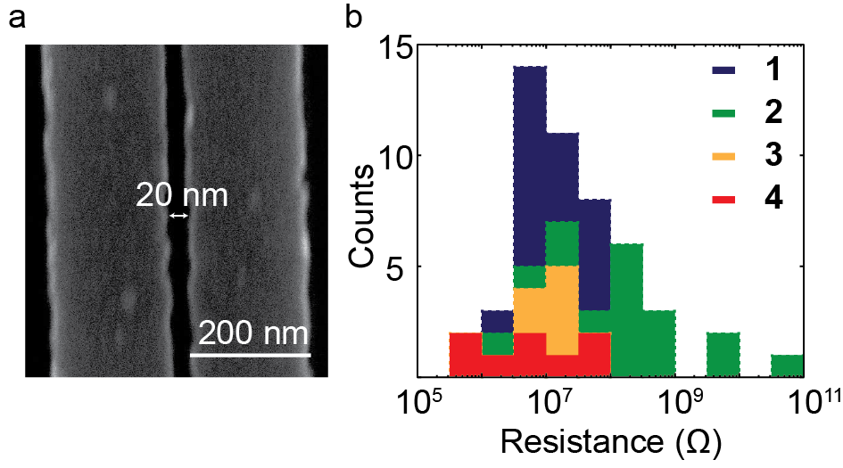
Figure 3a shows a scanning electron microscopy (SEM) image of a typical Pt nanogap with a feature size of 20 nm. 9-AGNRs with an average length of 45 nm and maximum lengths up to 100 nm are transferred onto these nanogaps, forming Pt-9-AGNR-Pt junctions. Here, we present electrical measurements of four different substrates, each contains multiple devices. Figure 3b summarizes the resistance of these junctions at 50 mV with all nanogap sizes.The junctions have a most probable low-bias resistance around , orders of magnitude lower than that in previous reports [12, 13, 14, 15, 20]. We also compare the low-bias resistance between junctions, made with a polymer-free transfer and PMMA-assisted transfer techniques on the same substrate (see Fig. S2). Consistently, the PMMA-assisted transferred junctions show a resistance that is 1 to 2 orders of magnitude higher, showing a clear influence of the use of PMMA on the transport properties, possibly due to different doping levels and contamination at the interfaces.
It is worth noting that the yield is nearly 100% for electrically conducting junctions, i.e., after GNR transfer. All devices were previously verified to be insulating. The large 9-AGNR/Pt contact area (1 m in vertical direction of Fig. 3a) may be of importance in this observation. A high yield benefiting from a large junction contact area was also observed previously, even in devices with m-size gaps [25]. This implies that the Pt-9-AGNR junctions comprise a network of GNRs, where a distance-dependent resistance is expected [25]. However, with the large spread in the resistance distribution, we do not observe significant difference in the low-bias resistance for devices with different nanogap sizes ranging from 20 nm to 100 nm (see Fig. S3).
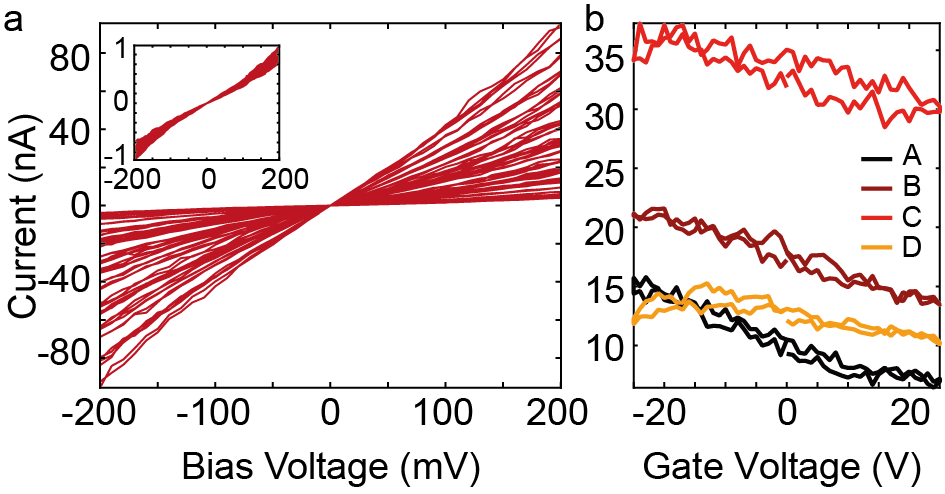
To gain more insight into charge transport in the 9-AGNR devices, we show the IV characteristics of sample 1 in Fig. 4 (see Fig. S4 for other samples). The current shows a linear dependence on the bias voltage within the range of 200 mV. To probe the linearity of the IV characteristics, we have applied a bias voltage up to 1 V, shown in Fig. S5 for sample 2. This bias limit is chosen to prevent the possible creation of filamentary paths in silicon oxide, which can occur at a few Volts applied across thin oxide layers [26]. In this case, we observe small nonlinearity taking place typically around a few hundred mV. The low resistance and nearly Ohmic s of these pre-patterned Pt-9-AGNR-Pt junctions can be a result of a better work function matching in comparison to previously investigated electrode materials [12, 13, 14, 15, 20].
Figure 4b shows the gate dependent current at a bias voltage of 100 mV. From the ratio of the maximum and minimum current for gate voltages ranging from -20 V to 20 V, the on-off ratio is determined: . We obtain small for sample 1. The highest on-off ratio of 25 is observed in sample 3, shown in Fig. S6d. Additional gate traces at a higher bias voltage of 1 V for sample 2 are shown in Fig. S7, where a maximum of 30 is observed. A crucial observation in the gate traces, consistent p-type transport, which is consistent with previous observations in 9-AGNR-based transistors [12, 13, 14, 15, 16, 25, 20].
The small gate dependence and on-off ratio of the current illustrate the poor gate efficiency of the 9-AGNR junctions. This poor efficiency may come from three contributions: (i) The electric field is screened by the metallic electrodes between the gate and GNR, and screened between GNR and GNR. These screening effects were demonstrated by simulations previously in ref. 16, where the electrostatic potential was completely screened in a densely packed GNR film with a GNR separation of 1.5 nm. It was also shown that a 20 nm nanogap is screened for more than 50% with an electrode thickness of 4 nm without the presence of GNRs [16]. This suggests that the densely packed 9-AGNR devices with a metal electrode height of 20 nm can be screened efficiently, leading to the observed poor gate efficiency. (ii) The low gate coupling is partially due to the low dielectric constant of the silicon oxide and the thick oxide thickness. An improvement for future experiments can be made by using a thin, high- gate oxide such as . (iii) The transport mechanism can be dominated by a hopping-like mechanism with an intrinsic low gate coupling. A temperature dependent measurement is necessary to elucidate the transport mechanism in these GNR devices, which is a subject of study for the future.
To describe the low resistance and nearly linear IV characteristics of the 9-AGNR junctions, we employed the density functional theory + non equilibirum Green’s function (DFT+NEGF) method to unveil the origin of this behavior in our 9-AGNR-Pt coupling. Details about the simulations can be found in SM.2.
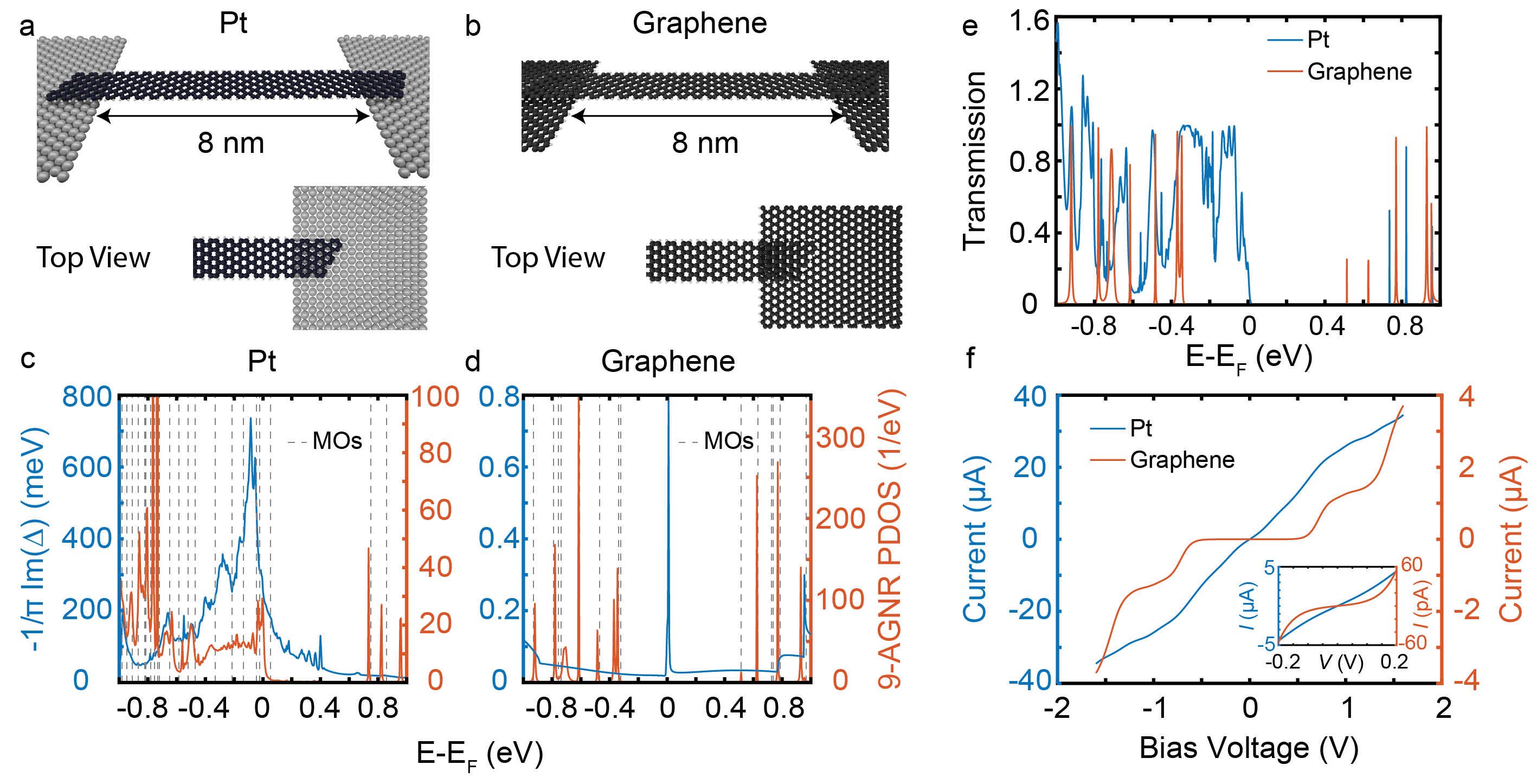
We consider the atomistic models in Figs. 5a and b. They are representative of a 9-AGNR contacted with platinum and graphene, respectively, with the goal of comparing both configurations. The length of the GNR is set to 11 nm and the contacts are separated by a 8-nm gap. For ribbons with atomically precise edges transport is expected to be ballistic and the conductance should not vary with the distance between the contacts [27]. To assess the quality of the latter we compute the hybridization strength of the GNR with the underlying electrodes and report the result in Figs. 5c-d. For platinum contacts, the hybridization is large below the Fermi level, i.e., in the valence band (VB) of the GNR, but decreases above this energy. This finding is evidenced by the density of states projected onto the GNR (PDOS), which evolves from a continuum of states below in the VB to a series of discrete and narrow peaks above it, directly linkable to the molecular orbital states (MOs) of the uncoupled GNR (vertical dashed lines).
For graphene contacts on the other hand, the hybridization remains small throughout the entire energy window relevant for transport and the PDOS strongly resembles the discrete spectrum of the dissociated GNR. This indicates that, upon contact with graphene, the electronic states in the channel remain mostly bounded. The hybridization strength is reflected in the electronic transmission (see Fig. 5e), which approaches the ideal constant value of 1 of a perfectly contacted GNR in the regions of large hybridization and reduces to sharp peaks typical of resonant transport otherwise. The current calculated by applying a symmetric bias across the electrodes shows a linear dependence for platinum contacts within the range of mV, in agreement with experiments (see Fig. 5f and 4a). In our calculations, the linear dependence stems from the -type character of the GNR - any bias window finds some open channels available for transport. Contrarily, the current for graphene contacts shows a non-linear, step-like behaviour typical of molecular junctions in the resonant transport regime in which the central molecule is loosely coupled to the leads.
Our simulation results thus indicate that, upon contact with platinum, the GNR MOs strongly hybridize with the underlying material and broaden into a continuous density of channels available for transport. This in turn yields devices with low contact resistance and nearly linear IV characteristic.
We fabricate 9-AGNR field effect transistor devices with Pt contacts by employing a polymer-free transfer technique subsequent to the deposition of electrical contacts. The GNR devices, ranging from 20 nm to 100 nm in gap width, consistently show a low-bias resistance value, , orders of magnitude lower than previous reports. Together with its nearly-Ohmic IV characteristics, the better device performance indicate that Pt electrodes with polymer-free transfer is ideal for 9-AGNR contacting. DFT+NEGF calculations demonstrate that Pt contact leads to a higher transmission than that other materials such as graphene. This not only explains the nearly linear characteristics and -type transport observed in the experiments, but also points out that Pt is a better contact material for a transparent contact interface.
Author Contributions
Chunwei Hsu: Conceptualization (equal); Methodology (equal); Validation (equal); Visualization (lead); Writing – original draft (lead); Writing – review & editing (lead).
Michael Rohde: Formal Analysis (lead); Validation (equal); Visualization (equal); Writing – review & editing (equal).
Gabriela Borin Barin: Resources (lead); Writing – original draft (equal); Writing – review & editing (equal).
Guido Gandus: Software (lead); Formal Analysis (equal); Methodology (equal); Writing – original draft (equal); Writing – review & editing (equal).
Daniele Passerone: Supervision (equal); Writing – review & editing (equal).
Mathieu Luisier: Supervision (equal); Writing – review & editing (equal).
Pascal Ruffieux: Funding Acquisition (equal); Supervision (equal); Writing – review & editing (equal).
Roman Fasel: Funding Acquisition (equal); Supervision (equal); Writing – review & editing (equal).
Herre S. J. van der Zan: Funding Acquisition (equal); Supervision (equal); Validation (equal); Writing – review & editing (equal).
Maria El Abbassi: Supervision (lead); Methodology (equal); Validation (lead); Writing – original draft (equal); Writing – review & editing (equal).
Acknowledgement
This study was supported by the EU and FET open project QuIET (number 767187). C. H. and H. S. J. v.d.Z. acknowledge The Netherlands Organization for Scientific Research (Natuurkunde Vrije Programma’s: 680.90.18.01). We acknowledge funding by the Swiss National Science Foundation under grant no. 200020-182015, the European Union Horizon 2020 research and innovation program under grant agreement no. 881603 (Graphene Flagship Core 3), and the Office of Naval Research BRC Program under the grant N00014-18-1-2708. We furthermore greatly appreciate the financial support from the Werner Siemens Foundation (Carbo Quant). DP, ML and GG acknowledge the NCCR MARVEL funded by the Swiss National Science Foundation (grant no. 51NF40-205602).
Data Availability Statement
The data that support the findings of this study are available from the corresponding author upon reasonable request.
References
References
- Saraswat, Jacobberger, and Arnold [2021] V. Saraswat, R. M. Jacobberger, and M. S. Arnold, “Materials Science Challenges to Graphene Nanoribbon Electronics,” ACS Nano 15, 3674–3708 (2021).
- Muñoz-Rojas, Fernández-Rossier, and Palacios [2009] F. Muñoz-Rojas, J. Fernández-Rossier, and J. J. Palacios, “Giant magnetoresistance in ultrasmall graphene based devices,” Physical Review Letters 102, 1–4 (2009), arXiv:0811.3831 .
- Magda et al. [2014] G. Z. Magda, X. Jin, I. Hagymási, P. Vancsó, Z. Osváth, P. Nemes-Incze, C. Hwang, L. P. Biró, and L. Tapasztó, “Room-temperature magnetic order on zigzag edges of narrow graphene nanoribbons,” Nature 514, 608–611 (2014).
- Li, Niquet, and Delerue [2016] J. Li, Y. M. Niquet, and C. Delerue, “Magnetic-Phase Dependence of the Spin Carrier Mean Free Path in Graphene Nanoribbons,” Physical Review Letters 116, 1–5 (2016).
- Son, Cohen, and Louie [2006] Y. W. Son, M. L. Cohen, and S. G. Louie, “Energy gaps in graphene nanoribbons,” Physical Review Letters 97, 1–4 (2006), arXiv:0611602 [cond-mat] .
- Schwierz [2010] F. Schwierz, “Graphene transistors,” Nature Nanotechnology 5, 487–496 (2010).
- Sevinçli, Topsakal, and Ciraci [2008] H. Sevinçli, M. Topsakal, and S. Ciraci, “Superlattice structures of graphene-based armchair nanoribbons,” Physical Review B - Condensed Matter and Materials Physics 78, 1–8 (2008).
- Baringhaus et al. [2014] J. Baringhaus, M. Ruan, F. Edler, A. Tejeda, M. Sicot, A. Taleb-Ibrahimi, A. P. Li, Z. Jiang, E. H. Conrad, C. Berger, C. Tegenkamp, and W. A. De Heer, “Exceptional ballistic transport in epitaxial graphene nanoribbons,” Nature 506, 349–354 (2014).
- Nakada et al. [1996] K. Nakada, M. Fujita, G. Dresselhaus, and M. S. Dresselhaus, “Edge state in graphene ribbons: Nanometer size effect and edge shape dependence,” Physical Review B 54, 17954–17961 (1996).
- Cao, Zhao, and Louie [2017] T. Cao, F. Zhao, and S. G. Louie, “Topological Phases in Graphene Nanoribbons: Junction States, Spin Centers, and Quantum Spin Chains,” Physical Review Letters 119, 1–5 (2017), arXiv:1702.02674 .
- Gröning et al. [2018] O. Gröning, S. Wang, X. Yao, C. A. Pignedoli, G. Borin Barin, C. Daniels, A. Cupo, V. Meunier, X. Feng, A. Narita, K. Müllen, P. Ruffieux, and R. Fasel, “Engineering of robust topological quantum phases in graphene nanoribbons,” Nature 560, 209–213 (2018), arXiv:1805.06635 .
- Bennett et al. [2013] P. B. Bennett, Z. Pedramrazi, A. Madani, Y. C. Chen, D. G. De Oteyza, C. Chen, F. R. Fischer, M. F. Crommie, and J. Bokor, “Bottom-up graphene nanoribbon field-effect transistors,” Applied Physics Letters 103, 1–5 (2013).
- Chen et al. [2016] Z. Chen, W. Zhang, C. A. Palma, A. Lodi Rizzini, B. Liu, A. Abbas, N. Richter, L. Martini, X. Y. Wang, N. Cavani, H. Lu, N. Mishra, C. Coletti, R. Berger, F. Klappenberger, M. Kläui, A. Candini, M. Affronte, C. Zhou, V. De Renzi, U. Del Pennino, J. V. Barth, H. J. Räder, A. Narita, X. Feng, and K. Müllen, “Synthesis of Graphene Nanoribbons by Ambient-Pressure Chemical Vapor Deposition and Device Integration,” Journal of the American Chemical Society 138, 15488–15496 (2016).
- Llinas et al. [2017] J. P. Llinas, A. Fairbrother, G. Borin Barin, W. Shi, K. Lee, S. Wu, B. Yong Choi, R. Braganza, J. Lear, N. Kau, W. Choi, C. Chen, Z. Pedramrazi, T. Dumslaff, A. Narita, X. Feng, K. Müllen, F. Fischer, A. Zettl, P. Ruffieux, E. Yablonovitch, M. Crommie, R. Fasel, and J. Bokor, “Short-channel field-effect transistors with 9-atom and 13-atom wide graphene nanoribbons,” Nature Communications 8, 8–13 (2017), arXiv:1605.06730 .
- Fairbrother et al. [2017] A. Fairbrother, J. R. Sanchez-Valencia, B. Lauber, I. Shorubalko, P. Ruffieux, T. Hintermann, and R. Fasel, “High vacuum synthesis and ambient stability of bottom-up graphene nanoribbons,” Nanoscale 9, 2785–2792 (2017).
- Mutlu et al. [2021] Z. Mutlu, Y. Lin, G. B. Barin, Z. Zhang, G. Pitner, S. Wang, R. Darawish, M. D. Giovannantonio, H. Wang, J. Cai, M. Passlack, C. H. Diaz, A. Narita, K. Mullen, F. R. Fischer, P. Bandaru, A. C. Kummel, P. Ruffieux, R. Fasel, and J. Bokor, “Short-Channel Double-Gate FETs with Atomically Precise Graphene Nanoribbons,” in 2021 IEEE International Electron Devices Meeting (IEDM) (IEEE, 2021) pp. 37.4.1–37.4.4.
- Ruffieux et al. [2016] P. Ruffieux, S. Wang, B. Yang, C. Sanchez-Sanchez, J. Liu, T. Dienel, L. Talirz, P. Shinde, C. A. Pignedoli, D. Passerone, T. Dumslaff, X. Feng, K. Müllen, and R. Fasel, “On-surface synthesis of graphene nanoribbons with zigzag edge topology,” Nature 531, 489–492 (2016).
- Keerthi et al. [2017] A. Keerthi, B. Radha, D. Rizzo, H. Lu, V. Diez Cabanes, I. C.-Y. Hou, D. Beljonne, J. Cornil, C. Casiraghi, M. Baumgarten, K. Müllen, and A. Narita, “Edge Functionalization of Structurally Defined Graphene Nanoribbons for Modulating the Self-Assembled Structures,” Journal of the American Chemical Society 139, 16454–16457 (2017).
- Borin Barin et al. [2022] G. Borin Barin, Q. Sun, M. Di Giovannantonio, C. Du, X. Wang, J. P. Llinas, Z. Mutlu, Y. Lin, J. Wilhelm, J. Overbeck, C. Daniels, M. Lamparski, H. Sahabudeen, M. L. Perrin, J. I. Urgel, S. Mishra, A. Kinikar, R. Widmer, S. Stolz, M. Bommert, C. Pignedoli, X. Feng, M. Calame, K. Müllen, A. Narita, V. Meunier, J. Bokor, R. Fasel, and P. Ruffieux, “Growth Optimization and Device Integration of Narrow‐Bandgap Graphene Nanoribbons,” Small 18, 2202301 (2022).
- Braun et al. [2021] O. Braun, J. Overbeck, M. El Abbassi, S. Käser, R. Furrer, A. Olziersky, A. Flasby, G. Borin Barin, Q. Sun, R. Darawish, K. Müllen, P. Ruffieux, R. Fasel, I. Shorubalko, M. L. Perrin, and M. Calame, “Optimized graphene electrodes for contacting graphene nanoribbons,” Carbon 184, 331–339 (2021), arXiv:2102.13033 .
- Li et al. [2018] R. Li, Z. Li, E. Pambou, P. Gutfreund, T. A. Waigh, J. R. P. Webster, and J. R. Lu, “Determination of PMMA Residues on a Chemical-Vapor-Deposited Monolayer of Graphene by Neutron Reflection and Atomic Force Microscopy,” Langmuir 34, 1827–1833 (2018).
- Fursina et al. [2008] A. Fursina, S. Lee, R. G. S. Sofin, I. V. Shvets, and D. Natelson, “Nanogaps with very large aspect ratios for electrical measurements,” Applied Physics Letters 92, 113102 (2008).
- Cai et al. [2014] J. Cai, C. A. Pignedoli, L. Talirz, P. Ruffieux, H. Söde, L. Liang, V. Meunier, R. Berger, R. Li, X. Feng, K. Müllen, and R. Fasel, “Graphene nanoribbon heterojunctions,” Nature Nanotechnology 9, 896–900 (2014).
- Borin Barin et al. [2019] G. Borin Barin, A. Fairbrother, L. Rotach, M. Bayle, M. Paillet, L. Liang, V. Meunier, R. Hauert, T. Dumslaff, A. Narita, K. Müllen, H. Sahabudeen, R. Berger, X. Feng, R. Fasel, and P. Ruffieux, “Surface-Synthesized Graphene Nanoribbons for Room Temperature Switching Devices: Substrate Transfer and ex Situ Characterization,” ACS Applied Nano Materials 2, 2184–2192 (2019).
- Richter et al. [2020] N. Richter, Z. Chen, A. Tries, T. Prechtl, A. Narita, K. Müllen, K. Asadi, M. Bonn, and M. Kläui, “Charge transport mechanism in networks of armchair graphene nanoribbons,” Scientific Reports 10, 1–8 (2020), arXiv:1806.00962 .
- Mehonic et al. [2018] A. Mehonic, A. L. Shluger, D. Gao, I. Valov, E. Miranda, D. Ielmini, A. Bricalli, E. Ambrosi, C. Li, J. J. Yang, Q. Xia, and A. J. Kenyon, “Silicon Oxide (SiO x ): A Promising Material for Resistance Switching?” Advanced Materials 30, 1801187 (2018).
- Koch et al. [2012] M. Koch, F. Ample, C. Joachim, and L. Grill, “Voltage-dependent conductance of a single graphene nanoribbon,” Nature nanotechnology 7, 713–717 (2012).