Far-Infrared Signatures for a Two-Steps Pressure-Driven Metallization in Transition Metal Dichalcogenides
Abstract
We present a high-pressure investigation of the semiconductor-to-metal transition in MoS2 and WS2 carried out by synchrotron-based far-infrared spectroscopy, to reconcile the controversial estimates of the metallization pressure found in the literature and gain new insight into the mechanisms ruling this electronic transition. Two spectral descriptors are found indicative of the onset of metallicity and of the origin of the free carriers in the metallic state: the absorbance spectral weight, whose abrupt increase defines the metallization pressure threshold, and the asymmetric lineshape of the E1u peak, whose pressure evolution, interpreted within the Fano model, suggests the electrons in the metallic state originate from n-type doping levels. Combining our results with those reported in the literature, we hypothesize a two-step mechanism is at work in the metallization process, in which the pressure-induced hybridization between doping and conduction band states drives an early metallic behaviour, while the band-gap closes at higher pressures.
I Introduction
Transition Metal Dichalcogenides (TMDs) are layered crystals that exhibit peculiar physical and chemical properties of great technological interest Manzeli2017 ; Choi2017 ; Mak2016 . These are mainly related to their crystalline structure made up of the stacking of weakly interacting planes. Planes are held together by strong covalent bonds while the interaction among them is mainly due to weak Van der Waals (VdW) forces. These materials are, thus, strongly anisotropic with respect to their mechanical, electrical and optical properties Johari2011 ; Kumar2012 .
The layered structure of TMDs makes the inter-layer interaction a key parameter governing their physical properties, from the lattice dynamics to the electronic structure Zhang2015 ; Sun2016 ; Yun2012 . In this perspective, the application of pressure provides an effective way to directly modulate the weak VdW forces linking adjacent layers, allowing getting a deeper insight into the fundamental physics of these materials and paving the way for a wide range of technological applications, in which the design of electronic devices with tailored features is of utmost interest Wang2015 ; Wang2012 .
Several pressure-dependent studies have been carried out aiming at studying the TMD response to a strong enhancement of the inter-layer interaction Dave2004 ; Bhattacharyya2012 ; PimentaMartins2022 ; Guo2013 . Most of the semiconducting crystals in the bulk form were found to undergo a pressure-induced transition toward a metallic state Fan2016 ; Zhao2019 ; Stellino2021 . However, in many cases, a certain degree of ambiguity persists in the exact determination of the metallization pressure as well as in the explanation of the microscopic origin of the transition.
In bulk MoTe2, resistivity measurements found evidence of the onset of a metallic behavior at 10-12 GPa Zhao2019 ; Yang2019 , while the effective closure of the band gap was observed at 24 GPa through absorption measurements in the near infrared (NIR) Stellino2022 . In a similar vein, resistivity Nayak2014 and impedance Zhuang2017 measurements carried out on bulk MoS2 suggested the crystal becomes metallic at 20 GPa, while absorption measurements in the NIR/visible range showed that the band gap closes at pressures higher than 26 GPa BrotonsGisbert2018 . As for the other semiconductors belonging to the class of TMDs, like WS2, in the majority of cases, the definition of the metallization threshold only relies on transport measurements Nayak2015 , while there lacks a direct estimate of the pressure-dependent trend of the band gap.
In the present work, we investigate the mechanisms at the origin of the metallic transition in semiconducting TMDs analysing, by synchrotron-based far-infrared (FIR) spectroscopy, the pressure-induced changes in the optical response of MoS2 and WS2. We found that the FIR spectrum can provide us with two effective descriptors that indicate both the onset of the metallic behaviour and the origin of the free charge carriers formed in the process. The first one is the absorbance spectral weight Stellino2021 ; Stellino2022 ; Postorino2003 ; Calvani1998 , whose abrupt increase under pressure defines the metallization threshold, , in good agreement with the results from resistivity measurements found in the literature for both compounds (in MoS2, 20 GPa Nayak2014 and 20 GPa, in WS2, 22 GPa Nayak2015 and 21 GPa). The second one is the lineshape of the E1u phonon, whose pressure evolution, interpreted in the framework of the Fano theory Fano1961 , suggests a reliable explanation for the origin of the free charge carriers in the metallic state. The asymmetric profile shown by the E1u phonon at ambient conditions is symptomatic of the coupling between the vibrational mode and a continuum of electronic transitions with comparable energy scales. In both MoS2 and WS2, these transitions cannot originate from a standard excitation from valence to conduction band, which is far too energetic ( eV) for the phonon (10-2 eV) to couple with, but they reasonably occur from doping levels located in the proximity of the conduction band minimum. Our measurements on MoS2 and WS2 show that, in correspondence with the increase in the absorbance spectral weight, the E1u peak abruptly symmetrizes, suggesting the energy separation between the doping levels and the conduction band minimum goes to zero.
Based on this phenomenology, our hypothesis is that the metallic behaviour we observed at 20 GPa and 21 GPa for MoS2 and WS2 respectively is driven by the injection of doping electrons in the conduction band, while the effective closure of the indirect band gap occurs at higher pressure, as indicated by NIR/visible optical measurements.
The pressure evolution of the MoS2 and WS2 absorbance spectra closely resembles that of MoTe2, previously studied and explained within the aforementioned scheme Stellino2022 . The observation of a similar phenomenology in three distinct compounds with three different metallization pressures might indicate that the observed behaviour is a common feature of semiconducting TMDs, suggesting the exploitation of our interpretation model in the general description of the metallic transition of these compounds.
II Experimental
MoS2 and WS2 single crystals were provided by HQ-Graphene. Measurements were performed on fresh-cut samples, directly cleaved from the macroscopic crystal to obtain flakes a few microns thick with a clean surface. It is worth noticing that, since the typical thickness of single-layer TMDs is 0.7 nm, in the present case, we safely work in the bulk limit.
Room temperature infrared transmission measurements on MoS2 were performed at the beamline SMIS of the SOLEIL synchrotron over the 0-26 GPa range. In the DAC, diamonds with 250 m culet were separated by a pre-indented, stainless steel, 50 m thick gasket, in which a hole of 125 m in diameter was drilled. Measurements were performed using a Thermo Fisher iS50 interferometer equipped with a solid-substrate beamsplitter. Synchrotron edge radiation was employed as a light source.
Custom-made 15x Cassegrain objectives with a large working distance allowed focusing and then collecting the transmitted radiation, finally detected by a liquid-helium-cooled bolometer detector.
Infrared transmission measurements on WS2 were performed at the beamline AILES of the SOLEIL synchrotron over the 0-25 GPa range. In the Diamond Anvil Cell (DAC), diamonds with 400 m culets were separated by a pre-indented stainless steel 50 m thick gasket, in which a hole of 150 m in diameter was drilled. Measurements were carried out using a Bruker IFS 125 HR interferometer, coupled with the synchrotron source, equipped with 15x Cassegrain objectives, a multi-layer Mylar 6 m beamsplitter and a liquid Helium cooled bolometer.
Both samples were positioned in the hole together with polyethylene (for WS2) or CsI (for MoS2) as a pressure transmitting media and a ruby chip, to measure the pressure through the ruby fluorescence technique.
At each pressure, the absorbance spectrum was obtained as
, where is the intensity transmitted with the sample loaded in the cell and is the background intensity with the DAC filled by the hydrostatic medium only.
III Evolution of the absorption spectral weight under pressure
As shown in figure 1, in both samples, all the measured curves display quite intense oscillating fringes due to interference effects between the internal diamond faces through the hydrostatic medium in . In this case, a Fourier transform smoothing procedure is not effective to remove the fringes owing to the reduced number of oscillation present in the spectrum. Besides the fringes, at ambient pressure, a sharp peak is well distinguishable at 380 cm-1 in MoS2 and at 350 cm-1 in WS2, assigned to the in-plane infrared phonon E1u. The phonon peak evolution under pressure will be discussed in detail in the next section, while, here, we will focus on the overall trend of the spectra. As we can notice, in both MoS2 (figure 1 a) and WS2 (figure 1 c), the average value, outside the phonon region, remains almost constant at low pressure and, then, abruptly rises above a pressure threshold, , around 20 GPa. In the framework of the Drude model, if , with and Drude relaxation time, the absorbance can be written in terms of the DC conductivity and the frequency as . In the FIR range here explored, we see that the Drude band contributes to the spectrum as a wavenumber-independent background, suggesting a relatively large value for compared to the values considered and, thus, allowing us to work within the low-wavenumber approximation. Based on these considerations, we can say that the increase we observed in the FIR absorbance is directly related to an increase in Stellino2021 ; Postorino2003 ; Calvani1998 and, thus, to the onset of the metallic behaviour reported in the resistivity measurements of both MoS2 and WS2 Nayak2014 ; Nayak2015 .
In order to quantitatively characterize this observation, we define at each pressure the absorption spectral weight as
. The trend of the normalized quantity , where
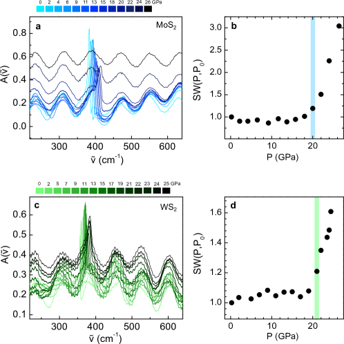
corresponds to the minimum pressure value measured in the two samples, is reported in figures 1 b,d for MoS2 and WS2 respectively. The integration is performed in the range 200-600 cm-1, but it excludes the small wavenumber interval where the phonon contribution is dominant. In the MoS2 case, we can notice a 30 of increase in at 20 GPa compared with the average value calculated at lower pressures. Therefore, we can define the metallization threshold GPa, in very good agreement with the results from resistivity measurements that observe the onset of the transition at 20 GPa Nayak2014 . As for the WS2 crystal, a 20 of increase is observed going from the 0-20 GPa range to 21 GPa, allowing us to place the metallization threshold at GPa. Again, this result is coherent with the transition pressure (22 GPa) found by resistivity measurements from the literature Nayak2015 .
A comparison between the spectral weight trends of the two samples reveals that the rate of increase of above is significantly higher in MoS2 than in WS2. Indeed, if we perform a linear fit of for values higher than we obtain a slope of 0.3 GPa-1 in the MoS2 trend and of 0.1 GPa-1 in the WS2 trend. This behaviour is consistent with the results from transport measurements on both samples Nayak2014 ; Nayak2015 , where the authors report an abrupt drop in the MoS2 resistivity () in correspondence with the metallization onset, while a more gradual decrease in was observed in the case of WS2.
IV Evolution of the Fano resonance under pressure
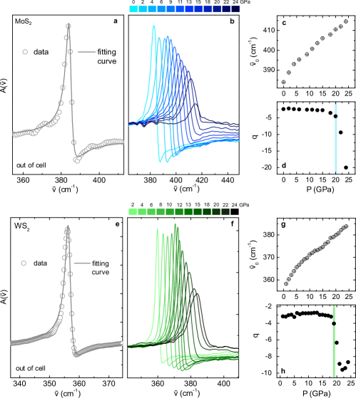
As seen in the previous section, FIR absorption spectra exhibit an intense peak at 380 cm-1 in MoS2 and at 350 cm-1 in WS2, both attributed to E1u vibrational modes. Figures 2a,e show the spectra of MoS2 and WS2, respectively, collected out of the DAC, in the wavenumber region around the phonon centre. In this configuration, the absence of interference fringes allows us to carefully examine the peak lineshape, which appears to significantly deviate from a standard Lorentzian in favour of a Fano-like profile.
The Fano theory, first introduced to describe the anomalous profile of the absorption peaks observed in the spectrum of He Fano1961 , describes, in general, the effects of the interaction between a discrete quantum state and a continuum of states with comparable energy scales. The model was reformulated by Rice et al. Rice1976 in terms of the so-called charged phonon theory, in which phonon modes with an asymmetric absorption profile are derived, under specific conditions, when the electron-phonon interaction is perturbatively inserted in the crystal Hamiltonian. In this framework, the gate-tunable asymmetric lineshape of the mode in graphene has been recently interpreted considering the coupling between the vibrational mode and the continuum formed by electron-hole transitions Cappelluti2009 ; Cappelluti2012 .
The close resemblance between TMDs and graphite in terms of lattice structure makes it possible, in principle, to interpret the phonon anomalies observed in the FIR spectrum of these crystals with the same model proposed for graphite, provided that we find suitable electronic excitations coupled with the phonon mode. In both MoS2 and WS2, the energy of standard valence-to-conduction band transitions is higher than 1.5-1.6 eV (that is the approximated value of the indirect gap of both samples), while the phonon energy, 40-65 meV, is nearly two orders of magnitude smaller. Therefore, a resonance between these two excitations is highly improbable. Since most of semiconducting TMDs are affected by a small percentage of n-type doping ( cm-3, as reported by the manufacturer HQ-Graphene), our hypothesis is that the electrons in excess may produce some extra levels right below the conduction band Leonhardt2020 ; Grzeszczyk2021 ; McCreary2016 ; Pisoni2015 . The thermal excitations from these levels to the empty states in the conduction band could be of the same energy scale of the phonon (indeed, meV and the phonon energies are lower than meV), providing the electron-phonon coupling mechanism responsible for the Fano lineshape observed in the absorption peaks.
Following this interpretation, we apply a fitting procedure for the phonon spectra of MoS2 and WS2 at ambient conditions using the Fano function reported here:
| (1) |
where is the peak centre, is the peak width and is the parameter associated with the line asymmetry. The symmetric Lorentzian profile, i.e. no resonance, is recovered in the limit .
The good agreement between the best fit curve and the experimental data out of the DAC (see figures 2 a,e for MoS2 and WS2 respectively) allows us to adopt a fitting procedure at higher pressures based on the combination of three functions: a polynomial background, a Fano-profile for the E1u phonon, and a sinusoidal curve for the interference fringes (some examples of the fitting procedure are provided in the supporting information). Figures 2 b,f show the spectra collected within the DAC at selected pressures after the background and fringes subtraction for MoS2 and WS2 respectively.
The parameters obtained from the data fit for the Fano profiles are reported in figure 2 c,d and in figure 2 g,h for MoS2 and WS2 respectively as a function of pressure. In both samples, the peak central frequency, , progressively moves toward higher wavenumbers on increasing pressure. This behaviour is coherent with what has been observed for the Raman-active counterpart of the E1u phonon, that is the E in-plane mode Nayak2014 ; Nayak2015 . In MoS2, the E1u intensity smoothly reduces in the low-pressure range and then rapidly goes to zero in the metallic regime. The screening of the phonon intensity could be regarded as a consequence of the optical response of free electrons, which progressively shield the phonon contribution in the FIR absorption Stellino2020 . As for the peak profile, figure 2 d clearly shows that the parameter keeps almost constant () for low-pressure values; then, above P18 GPa, just before the spectral weight growth observed before, the modulus of rapidly increases and the peak symmetrizes. Similarly, in WS2, we observe a nearly constant trend for the peak intensity up to 15 GPa, followed by an intensity reduction for higher pressure values. Regarding the peak profile, the parameter maintains a nearly constant value () in the semiconducting regime. Then, just before the onset of the metallic behaviour, the modulus of abruptly increases leading to the peak symmetrization, in analogy with the MoS2 sample.
Based on the previous discussion, the evolution of the parameter in the peak profile can be considered a benchmark to evaluate the response of the doping levels to the applied pressure. In particular, the peak symmetrization implies the occurrence of an electronic configuration in which transitions from intra-gap states to conduction band cannot take place. In this perspective, our hypothesis is that the pressure evolution of the sample band structure leads to a progressive reduction of the energy separation between conduction and doping states until the latter ones overlap in correspondence with the metallization pressure . Once doping levels are hybridized with the conduction band, no more direct electronic transitions from intra-gap states are available for the phonon to couple with, preventing the observation of the Fano resonance in the E1u profiles.
V Discussion and conclusion
The present work was devoted to the spectroscopic study of the metallic transition in MoS2 and WS2 under pressure in the far infrared range.
The analysis of the spectral weight under pressure proved itself as a robust, reliable indicator of the onset of the metallic behavior in both compounds, providing us with an estimate of the metallization pressure perfectly compatible with that obtained by transport measurements. The SW trends also gave us a semi-quantitative information on the different rate of increase of the DC conductivity in the two crystals, suggesting a slower transition in WS2 compared with the MoS2 case, in agreement with the results from resistivity measurements. It is worth noticing that a similar analysis conducted on Mo0.5W0.5S2 Stellino2021 gave a metallization threshold very close to the average of MoS2 and WS2, which is exactly what would be expected for an alloy compound. Moreover, a good correspondence between the metallization onset obtained from pressure-dependent FIR measurements and pressure-dependent transport measurements was found for MoTe2 Stellino2022 . These results obtained on three different TMD semiconductors and a TMD alloy indicate the SW analysis of the FIR spectrum as a reliable approach for the detection of the metallic behavior in this class of materials. Compared with transport measurements, FIR transmission measurements allow working with constant room temperature and offer the advantage of an easier assembly of the DAC, although they do not enable for a quantitative estimate of physical quantities as the carrier density and mobility.
Regarding the analysis of the phonon modes, the asymmetric profile, shown by the E1u peak at ambient conditions, was modelled in the framework of the Fano theory and interpreted as symptomatic of the coupling between the vibrational mode and a continuum of electronic transitions with comparable energy scales. These transitions cannot originate from a standard
excitation from valence to conduction band, which is far too energetic for the phonon to couple with, but they reasonably occur from doping levels located in the proximity of the conduction band minimum. Based on this consideration, the pressure evolution of the Fano resonance can provide us with a unique benchmark to evaluate the response of these doping levels to the applied pressure. In particular, our measurements on MoS2 and WS2 show that the asymmetry parameter extracted from the Fano fit of the phonon line remains finite and nearly constant in the semiconducting regime; then, just before the onset of the metallic behaviour, the peak abruptly symmetrizes suggesting the energy separation between the doping levels and the conduction band minimum goes to zero.
Following the results obtained from the analysis of the Fano resonance in the phonon peaks, we propose an alternative scenario for the metallization process in MoS2 and WS2, in which the metallic behavior at is driven by the pressure-induced overlap between doping levels and conduction band minimum, while the electronic band gap is still open. In order to observe the effective closure of the band gap, we would need to further increase the applied pressure, until valence and conduction band cross the Fermi level. This interpretation model, analogous to that proposed for the metallization process in MoTe2 Stellino2022 , can explain the coincidence between the spectral weight increase and the phonon peak symmetrization under pressure in the measured samples. Moreover, it allows reconciling the apparently controversial results reported in the literature on MoS2, where NIR/visible absorption measurements found a gap closing pressure significantly higher with respect to the metallization pressure obtained by transport measurements and by our FIR measurements. Indeed, absorption spectroscopy in the NIR/visible gives us information about the evolution of the main electronic transition without being affected by the presence of low-energy excitation from extra doping levels. Conversely, transport and FIR measurements are sensible to the increase in the sample conductivity, which might arise independently on the evolution of the valence and conduction band extremes.
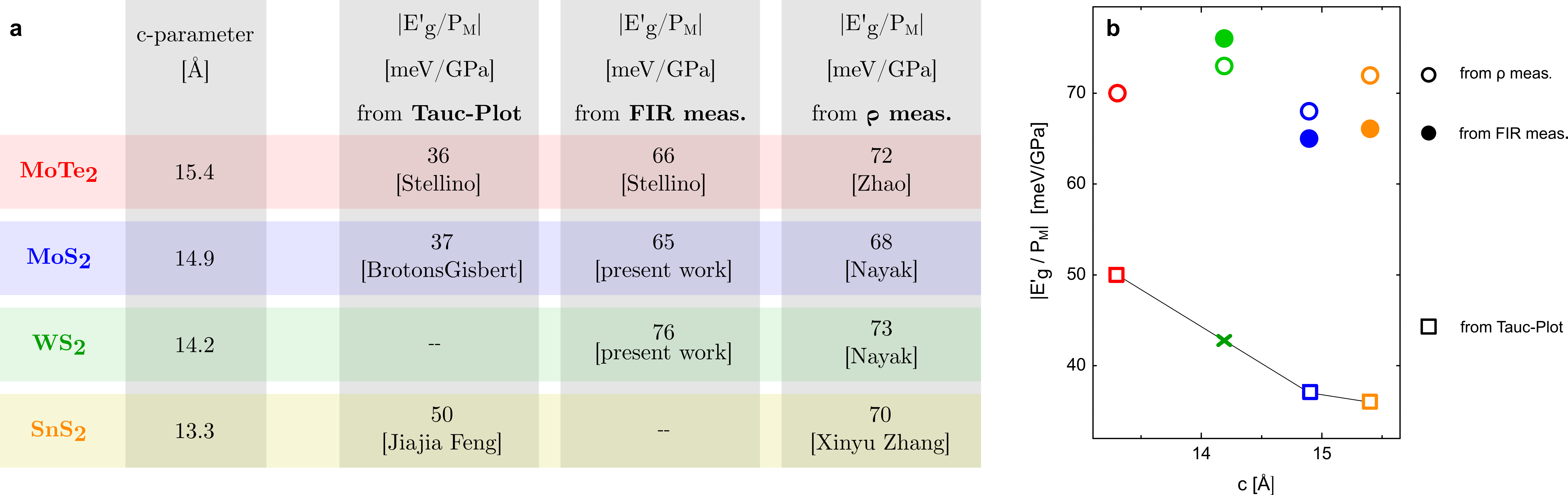
To further corroborate our hypothesis, we report in figure 3(a) different estimates of , in which is the indirect gap energy at ambient pressure and the values are the metallization pressures found by Tauc-plot extrapolation in the NIR/visible range, by absorption measurements in the FIR, and by transport measurements, for MoTe2, MoS2, WS2 and SnS2.
As shown in figure 3(b), the value of obtained by Tauc-plot extrapolation steadily increases as the c-parameter of the considered material decreases. The mutual dependence between and c supports the idea that the metallization threshold found in this case corresponds to the actual gap-closing pressure. Indeed, in TMD semiconductors, the band extremes involved in the indirect gap are dominated by out-of-plane orbitals (like the from the chalcogen atoms) Cappelluti2013 ; Kadantsev2012 , which are particularly sensitive to variations in the inter-layer distance. Therefore, the trend of the indirect band gap under pressure is expected to show some kind of correlation with the c-parameter, which defines inter-layer distance at ambient conditions.
In the same perspective, the absence of a clear dependence in the trends of versus the c-parameter obtained by FIR and transport measurements, very close to each other, corroborates the hypothesis that the metallic behaviour observed in these experiments is driven by doping effects which are not strictly related to the evolution of the indirect band gap.
To sum up, high pressure FIR measurements on MoS2 and WS2 enabled us to gain a deeper insight into the evolution of the electronic properties of semiconducting TMDs. Based on the obtained results, our idea is that the pressure-induced metallization process in these compounds comprises two distinct charge delocalization processes: the first one, here observed, driven by the reduction in the energy separation between doping levels and conduction band; the second one, taking place at higher pressures, driven by the reduction in the energy separation between valence band maximum and conduction band minimum. The observation of a nearly identical phenomenology in both MoS2 and WS2, not to mention the similar results obtained on MoTe2 in the literature, might indicate that the presence of unintentional doping levels plays a key role in the pressure evolution of the electronic properties of most of semiconducting TMDs and thus must be carefully considered in all experimental works aiming at studying metallization processes in this class of materials.
References
- (1) Sajedeh Manzeli, Dmitry Ovchinnikov, Diego Pasquier, Oleg V. Yazyev, and Andras Kis. 2d transition metal dichalcogenides. Nature Reviews Materials, 2(8), June 2017.
- (2) Wonbong Choi, Nitin Choudhary, Gang Hee Han, Juhong Park, Deji Akinwande, and Young Hee Lee. Recent development of two-dimensional transition metal dichalcogenides and their applications. Materials Today, 20(3):116–130, April 2017.
- (3) Kin Fai Mak and Jie Shan. Photonics and optoelectronics of 2D semiconductor transition metal dichalcogenides. Nature Photonics, 10(4):216–226, March 2016.
- (4) Priya Johari and Vivek B. Shenoy. Tunable dielectric properties of transition metal dichalcogenides. ACS Nano, 5(7):5903–5908, July 2011.
- (5) Ashok Kumar and P.K. Ahluwalia. Tunable dielectric response of transition metals dichalcogenides MX2 (m=mo,w x=s,se,te): Effect of quantum confinement. Physica B: Condensed Matter, 407(24):4627–4634, December 2012.
- (6) Xin Zhang, Xiao-Fen Qiao, Wei Shi, Jiang-Bin Wu, De-Sheng Jiang, and Ping-Heng Tan. Phonon and raman scattering of two-dimensional transition metal dichalcogenides from monolayer, multilayer to bulk material. Chemical Society Reviews, 44(9):2757–2785, 2015.
- (7) Yajing Sun, Dong Wang, and Zhigang Shuai. Indirect-to-direct band gap crossover in few-layer transition metal dichalcogenides: A theoretical prediction. The Journal of Physical Chemistry C, 120(38):21866–21870, September 2016.
- (8) Won Seok Yun, S. W. Han, Soon Cheol Hong, In Gee Kim, and J. D. Lee. Thickness and strain effects on electronic structures of transition metal dichalcogenides. Physical Review B, 85(3), January 2012.
- (9) Haotian Wang, Hongtao Yuan, Seung Sae Hong, Yanbin Li, and Yi Cui. Physical and chemical tuning of two-dimensional transition metal dichalcogenides. Chemical Society Reviews, 44(9):2664–2680, 2015.
- (10) Qing Hua Wang, Kourosh Kalantar-Zadeh, Andras Kis, Jonathan N. Coleman, and Michael S. Strano. Electronics and optoelectronics of two-dimensional transition metal dichalcogenides. Nature Nanotechnology, 7(11):699–712, November 2012.
- (11) Madhavi Dave, Rajiv Vaidya, S. G. Patel, and A. R. Jani. High pressure effect on MoS2 and MoSe2 single crystals grown by CVT method. Bulletin of Materials Science, 27(2):213–216, April 2004.
- (12) Swastibrata Bhattacharyya and Abhishek K. Singh. Semiconductor-metal transition in semiconducting bilayer sheets of transition-metal dichalcogenides. Physical Review B, 86(7), August 2012.
- (13) Luiz G. Pimenta Martins, Bruno R. Carvalho, Connor A. Occhialini, Natália P. Neme, Ji-Hoon Park, Qian Song, Pedro Venezuela, Mário S. C. Mazzoni, Matheus J. S. Matos, Jing Kong, and Riccardo Comin. Electronic band tuning and multivalley raman scattering in monolayer transition metal dichalcogenides at high pressures. ACS Nano, April 2022.
- (14) Huaihong Guo, Teng Yang, Peng Tao, Yong Wang, and Zhidong Zhang. High pressure effect on structure, electronic structure, and thermoelectric properties of MoS2. Journal of Applied Physics, 113(1):013709, January 2013.
- (15) Xaiofeng Fan, David J. Singh, Q. Jiang, and W. T. Zheng. Pressure evolution of the potential barriers of phase transition of MoS2 and MoTe2. Physical Chemistry Chemical Physics, 18(17):12080–12085, 2016.
- (16) X. M. Zhao, H. Y. Liu, A. F. Goncharov, Z. W. Zhao, V. V. Struzhkin, H. K. Mao, A. G. Gavriliuk, and X. J. Chen. Pressure effect on the electronic, structural, and vibrational properties of layered 2HMoTe2. Phys. Rev. B, 99:024111, 2019.
- (17) Elena Stellino, Francesca Ripanti, Giacomo Nisini, Francesco Capitani, Caterina Petrillo, and Paolo Postorino. Infrared study of the pressure-induced isostructural metallic transition in Mo0.5W0.5S2. The Journal of Physical Chemistry C, 125(28):15503–15509, July 2021.
- (18) Linfei Yang, Lidong Dai, Heping Li, Haiying Hu, Kaixiang Liu, Chang Pu, Meiling Hong, and Pengfei Liu. Characterization of the pressure-induced phase transition of metallization for MoTe2 under hydrostatic and non-hydrostatic conditions. AIP Adv., 9(6):065104, 2019.
- (19) E. Stellino, F. Capitani, F. Ripanti, M. Verseils, C. Petrillo, P. Dore, and P. Postorino. Broadband infrared study of pressure-tunable fano resonance and metallization transition in 2H-MoTe2. Scientific Reports, 12(1), October 2022.
- (20) Avinash P. Nayak, Swastibrata Bhattacharyya, Jie Zhu, Jin Liu, Xiang Wu, Tribhuwan Pandey, Changqing Jin, Abhishek K. Singh, Deji Akinwande, and Jung-Fu Lin. Pressure-induced semiconducting to metallic transition in multilayered molybdenum disulphide. Nature Communications, 5(1), May 2014.
- (21) YuKai Zhuang, LiDong Dai, Lei Wu, HePing Li, HaiYing Hu, KaiXiang Liu, LinFei Yang, and Chang Pu. Pressure-induced permanent metallization with reversible structural transition in molybdenum disulfide. Applied Physics Letters, 110(12):122103, March 2017.
- (22) Mauro Brotons-Gisbert, Alfredo Segura, Roberto Robles, Enric Canadell, Pablo Ordejón, and Juan F. Sánchez-Royo. Optical and electronic properties of 2H-MoS2 under pressure: Revealing the spin-polarized nature of bulk electronic bands. Physical Review Materials, 2(5), May 2018.
- (23) Avinash P. Nayak, Zhen Yuan, Boxiao Cao, Jin Liu, Junjie Wu, Samuel T. Moran, Tianshu Li, Deji Akinwande, Changqing Jin, and Jung-Fu Lin. Pressure-modulated conductivity, carrier density, and mobility of multilayered tungsten disulfide. ACS Nano, 9(9):9117–9123, August 2015.
- (24) P. Postorino, A. Congeduti, P. Dore, A. Sacchetti, F. Gorelli, L. Ulivi, A. Kumar, and D. D. Sarma. Pressure tuning of electron-phonon coupling: The insulator to metal transition in manganites. Physical Review Letters, 91(17):175501, October 2003.
- (25) P. Calvani, G. De Marzi, P. Dore, S. Lupi, P. Maselli, F. D'Amore, S. Gagliardi, and S-W. Cheong. Infrared absorption from charge density waves in magnetic manganites. Physical Review Letters, 81(20):4504–4507, November 1998.
- (26) U. Fano. Effects of configuration interaction on intensities and phase shifts. Phys. Rev., 124(6):1866, 1961.
- (27) M. J. Rice. Organic linear conductors as systems for the study of electron-phonon interactions in the organic solid state. Physical Review Letters, 37(1):36–39, July 1976.
- (28) A. B. Kuzmenko, L. Benfatto, E. Cappelluti, I. Crassee, D. van der Marel, P. Blake, K. S. Novoselov, and A. K. Geim. Gate tunable infrared phonon anomalies in bilayer graphene. Phys. Rev. Lett., 103:116804, 2009.
- (29) E. Cappelluti, L. Benfatto, M. Manzardo, and A. B. Kuzmenko. Charged-phonon theory and Fano effect in the optical spectroscopy of bilayer graphene. Phys. Rev. B, 86:115439, 2012.
- (30) Alessandra Leonhardt, César Javier Lockhart Rosa, Thomas Nuytten, Luca Banszerus, Stefanie Sergeant, Vivek K. Mootheri, Takashi Taniguchi, Kenji Watanabe, Christoph Stampfer, Cedric Huyghebaert, and Stefan De Gendt. Use of the indirect photoluminescence peak as an optical probe of interface defectivity in MoS2. Advanced Materials Interfaces, 7(18):2000413, August 2020.
- (31) Magdalena Grzeszczyk, Katarzyna Olkowska-Pucko, Karol Nogajewski, Kenji Watanabe, Takashi Taniguchi, Piotr Kossacki, Adam Babiński, and Maciej R. Molas. Exposing the trion’s fine structure by controlling the carrier concentration in hBN-encapsulated MoS2. Nanoscale, 13(44):18726–18733, 2021.
- (32) Kathleen M. McCreary, Aubrey T. Hanbicki, Simranjeet Singh, Roland K. Kawakami, Glenn G. Jernigan, Masa Ishigami, Amy Ng, Todd H. Brintlinger, Rhonda M. Stroud, and Berend T. Jonker. The effect of preparation conditions on raman and photoluminescence of monolayer WS2. Scientific Reports, 6(1), October 2016.
- (33) A. Pisoni, J. Jacimovic, O. S Barissic̀, A. Walter, B. Nàfràdi, P. Bugnon, A. Magrez, H. Berger, Z. Revay, and L. Forrò. The role of transport agents in MoS2 single crystals. J. Phys. Chem. C, 119(8):3918–3922, 2015.
- (34) E Stellino. Pressure evolution of the optical phonons of mote2. Il nuovo cimento C, 43(4-5):1–8, 2020.
- (35) Jiajia Feng, Cong Li, Wen Deng, Bencheng Lin, Wenhui Liu, Resta A. Susilo, Hongliang Dong, Zhiqiang Chen, Nan Zhou, Xiaolei Yi, Xiangzhuo Xing, Feng Ke, Zhenxian Liu, Hongwei Sheng, Zhixiang Shi, and Bin Chen. Superconductivity induced by lifshitz transition in pristine SnS2 under high pressure. The Journal of Physical Chemistry Letters, 13(40):9404–9410, October 2022.
- (36) Xinyu Zhang, Lidong Dai, Haiying Hu, Meiling Hong, and Chuang Li. Pressure-induced coupled structural–electronic transition in SnS2 under different hydrostatic environments up to 39.7 GPa. RSC Advances, 12(4):2454–2461, 2022.
- (37) Anubhav Jain, Shyue Ping Ong, Geoffroy Hautier, Wei Chen, William Davidson Richards, Stephen Dacek, Shreyas Cholia, Dan Gunter, David Skinner, Gerbrand Ceder, and Kristin A. Persson. Commentary: The materials project: A materials genome approach to accelerating materials innovation. APL Materials, 1(1):011002, July 2013.
- (38) E. Cappelluti, R. Roldán, J. A. Silva-Guillén, P. Ordejón, and F. Guinea. Tight-binding model and direct-gap/indirect-gap transition in single-layer and multilayer MoS2. Physical Review B, 88(7), August 2013.
- (39) Eugene S. Kadantsev and Pawel Hawrylak. Electronic structure of a single MoS2 monolayer. Solid State Communications, 152(10):909–913, May 2012.