Bottom-up growth of monolayer honeycomb SiC
Abstract
The long theorized two-dimensional allotrope of SiC has remained elusive amid the exploration of graphenelike honeycomb structured monolayers. It is anticipated to possess a large direct band gap (2.5 eV), ambient stability, and chemical versatility. While bonding between silicon and carbon is energetically favorable, only disordered nanoflakes have been reported to date. Here we demonstrate large-area, bottom-up synthesis of monocrystalline, epitaxial monolayer honeycomb SiC atop ultrathin transition metal carbide films on SiC substrates. We find the 2D phase of SiC to be almost planar and stable at high temperatures, up to 1200℃ in vacuum. Interactions between the 2D-SiC and the transition metal carbide surface result in a Dirac-like feature in the electronic band structure, which in the case of a TaC substrate is strongly spin-split. Our findings represent the first step towards routine and tailored synthesis of 2D-SiC monolayers, and this novel heteroepitaxial system may find diverse applications ranging from photovoltaics to topological superconductivity.
Chemical bonding between C and Si may exhibit competition between the hybridization preferred by silicon and the hybridization preferred by carbonMelion2007 . Nonetheless, first-principles calculations predict that two-dimensional, bonded SiC (2D-SiC) should be stable, with the planar, stoichiometric structure the most energetically favorable conformationSahin2009 ; Huda2009 ; Zhou2013 ; Shi2015 . Despite considerable interest in its properties and several theoretical studiesChabi2020 ; Lu2012 ; Lin2013 ; Hsueh2011 , experimental synthesis of 2D-SiC has proven difficultLin2012 ; Susi2017 ; Chabi2021 . Central to this challenge is that, unlike graphitic carbon, bulk SiC does not exist in a layered form and hence does not lend itself to top-down exfoliation techniques.
Here we demonstrate a bottom-up approach to the synthesis of 2D-SiC, by preparing ultra thin carbide films (t3 nm) on SiC substrates followed by annealing to high temperature (T1700℃), similar to the process used for epitaxial growth of graphene on SiC. Underlying this approach is our ability to produce high-quality ultra thin epitaxial films of transition metal carbides on the silicon terminated face of 4H-SiC. Carbides are well known for their extreme thermal, chemical and mechanical robustness, and among the transition metal carbides TaC and NbC in particular have received renewed attention owing to their bulk superconductivity (TC 11 K) and topologically nontrivial electronic band structure Shang2020 ; Cui2020 ; Yan2021 . Both TaC and NbC can grow epitaxially on 4H-SiC, as they have a rocksalt crystal structure with a threefold symmetric (111) plane that is nearly lattice matched to 4H-SiC (0001) (2.3% and 2.7% lattice mismatch, respectively). Huder et. al. reported a bottom-up solid state reaction in which films of Ta on a SiC substrate were transformed into graphene-terminated TaC by thermal annealing, with carbon being sourced from the decomposing SiC LeQuang2017 ; Huder2018 . While the simplicity of this approach is appealing, the resulting TaC film is polycrystalline with grain sizes of 200 nm2. We have developed an alternative process involving sputter deposition of approximately ten monolayers of transition metal carbide followed by annealing to 1700℃ in an Ar atmosphere. Directly depositing a carbide rather than the base metal ensures a stoichiometric film and recrystallization upon annealing. Remarkably, we observe that while the annealing step indeed structurally orders the carbide, in addition it leaves the surface terminated with a monolayer of honeycomb SiC.
Results
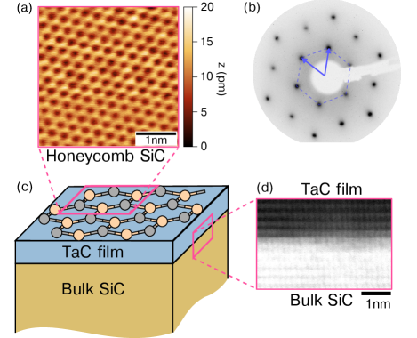
The samples studied are schematically depicted in Figure 1a. They consist of 3 nm thick films of TaC or NbC sputter deposited onto Si-terminated 4H-SiC(0001) substrates, with a lateral extent of approximately 5 mm 5 mm. The deposition was followed by a 1700℃ anneal for 10 min in an Ar atmosphere. Here we mainly focus on TaC, but later will show that a similar result is obtained from NbC. The TaC/SiC interface is abrupt and the films are epitaxial, as revealed by cross-sectional high-angle annular dark-field scanning transmission electron microscopy (HAADF-STEM). Cubic TaC has a rocksalt crystal structure with lattice parameter a=4.456ÅToth1971 , which presents {111} facets with an in-plane lattice parameter a=3.15Å, readily accommodated atop the SiC substrate with a=3.08Å. Stockmeier2009 . While hexagonal (Ta2C) or ternary (Ta2SiC) phases are in principle possible, there are several indications that the films as grown take the simple rocksalt structure. The HAADF-STEM (Figure 1d) shows cubic ordering, and the measured superconducting transition temperature of 9-10 K (see Supplementary Material) is consistent with cubic, stoichiometric TaC Giorgi1962 . After transferring the samples into UHV and briefly annealing at 1000℃ to remove surface oxidation, sharp hexagonal spots in LEED (Figure 1b) and bands in ARPES (Figure 2) become visible. Scanning tunneling microscopy (STM) (Figure 1a) indicates a hexagonal surface lattice with a=(3.120.04)Å, uniformly covering the millimeter-scale sample (see Supplementary Material for additional topographic images) . This surface is robust against longer or repeated heating cycles to similar temperatures, but at much higher temperatures will begin to transform into graphene (see Supplementary Material).
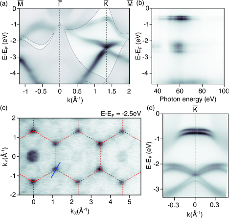
The most striking features in the ARPES measurements are spin-split surface states within a large surface-projected band gap of the TaC (Figure 2a). Photon energy scans (Figure 2b) demonstrate the 2D character of these states, while constant-energy surfaces (Figure 2c) confirm a 11 hexagonal surface lattice (overlaid in red). The zone size (- = 1.34Å-1) agrees with the lattice constant observed in STM. A high-resolution cut through (Figure 2d) clearly illustrates the spin-orbit splitting of the bands, which reaches 125 meV for the upper bands and 220 meV for the lower set. All of these states are completely occupied, with the Fermi surface dominated by TaC bulk states spanning most of the surface Brillouin zone.
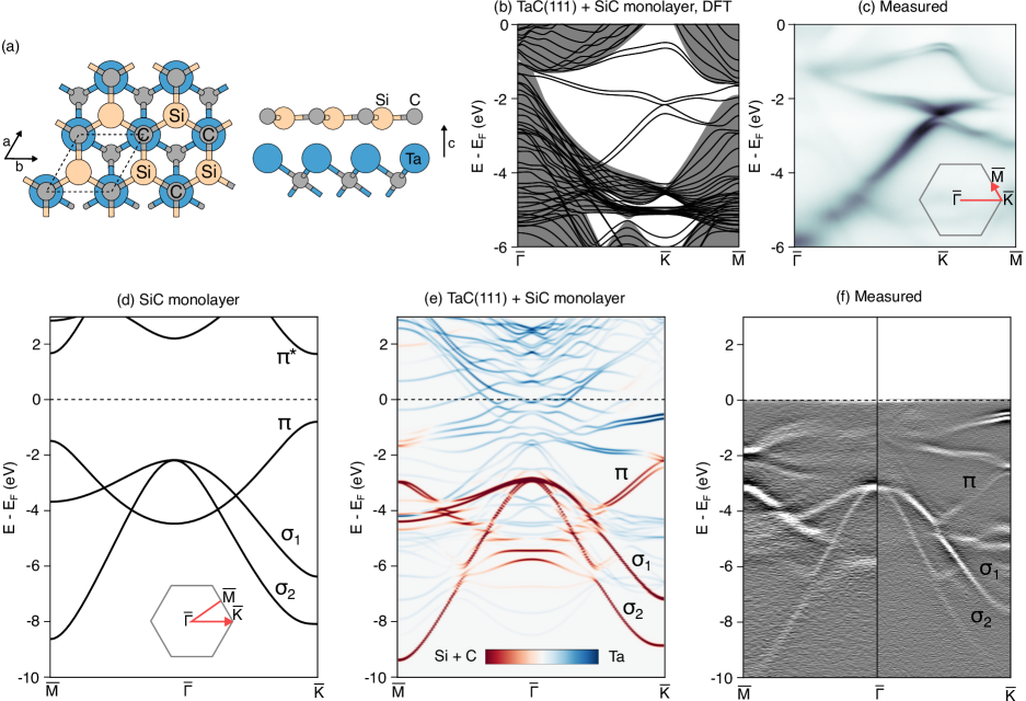
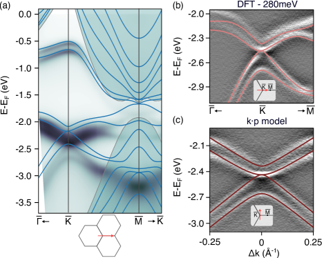
Based on evidence offered by LEED, STM, core levels (described below) and particularly DFT band structure calculations, we conclude that the ARPES measurements can only be explained by the presence of a monolayer of honeycomb SiC. The proposed structure is depicted in Figure 3a, and generates a calculated band structure that is in excellent agreement with experimental spectra (Figure 3b,c). The registry of the SiC monolayer has carbon atoms atop the substrate Ta atoms and silicon atoms in an fcc-hollow position. After relaxation along the c axis the SiC layer is weakly buckled ( = 16.8 pm) and located 2.3Å above the surface layer of Ta atoms. In order for the DFT model to reproduce the degeneracy at the buckling must be reduced to 11.8 pm (see Supplementary Information). Unlike silicene (44 pm), the 2D-SiC here is nearly planar.
To interpret the band structure calculations it is helpful to draw comparisons with an isolated, planar honeycomb SiC monolayer (Figure 3d). Quite unlike its semimetallic relatives graphene or (planar) silicene, honeycomb SiC features a large band gap between the and * bands. In Figure 3e we plot the atom-, layer- and -resolved band structure, obtained by projecting the calculated wave functions onto the topmost two atomic layers of the slab (Si, C, and Ta atoms). This suppresses the bulklike TaC slab bands and thereby mimics the surface sensitivity of an ARPES measurement. We additionally use a color scale to represent the atomic character of each state. Presented in this manner, the SiC and bands become obvious both in the calculations and in experimental spectra (Figure 3g). We can furthermore identify the valence band of the Dirac-like surface state as deriving from the SiC band, while the conduction band and also the uppermost surface state have strong Ta 5d orbital character. The hybridization of the band, together with the large spin-orbit splitting, makes it clear that the SiC layer is strongly interacting with the TaC substrate.
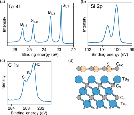
Core level spectroscopy measurements (Figure 4a-c) are consistent with the proposed structure in Figure 3a. The only species observed on the surface are Ta, Si and C, and none are trace impurities - when measured together at h = 650 eV the cross-section adjusted intensity ratio is Ta:Si:C = 0.4:0.25:1. The Ta 4f core level spectrum (Figure 4a) consists of bulk () and surface () doublets, consistent with previous studies of {111} facets of bulk transition metal carbides that uniformly find a metal element rather than carbon termination Johansson1995 . While the position of our doublet is in excellent agreement with stoichiometric bulk TaC Gruzalski1986 , the bulk-surface doublet splitting is approximately 250 meV smaller than would be expected from a simple TaC(111) surface Johansson1995 . The Si 2p spectrum (Figure 4b) consists of a single doublet and derives from silicon atoms close to the surface. This photon energy (130 eV) could in principle be weakly sensitive to silicon at the buried interface with the bulk SiC substrate, but this is unlikely to be the origin of the Si peak given that it shows an abrupt shift in binding energy when the surface oxide is removed (Supplementary Material). The C 1s spectrum (Figure 4c) contains three components, of which the component alone is closely correlated with the presence of the honeycomb SiC band structure. The other two components exist both before the SiC termination is established and after it is eliminated (see Supplementary Material). One of these peaks () can be assigned to bulk carbon in the TaC film, with a binding energy in good agreement with measurements from the (001) surface of a bulk TaC crystalGruzalski1986 . Figure 4d suggests origins for each component.
Discussion
While the overall agreement between the DFT calculations and ARPES measurements is excellent, there are two notable exceptions concerning the Dirac-like feature at . The first concerns the experimentally observed degeneracy - after full relaxation of the slab along the c-axis, band calculations rather predict a sizeable band gap of 200 meV. This can be resolved by reducing the buckling of the SiC monolayer from 16.8 pm to 11.8 pm, which is still larger than the 5 pm suggested by STM (see Supplementary Material). While it is interesting that the real system apparently assumes precisely the buckling that results in a band degeneracy at , the gap being a continuously tunable function of the buckling argues against the existence of a symmetry protection. The second exception concerns the binding energy of this feature, which requires a rigid shift of 280 meV to higher values to agree with experiments (Figure 5c). The Ta 5d derived surface state at lower binding energy does not require such a shift. We assume that these discrepancies can be resolved with a more sophisticated calculation method (e.g. DFT+U) or with a more complex structural model (e.g. including a buffer layer).
Close to the Dirac-like degeneracy at , it is possible to alternatively describe the dispersion using the kp model originally suggested for incorporating spin-orbit coupling effects into the graphene Dirac-cone dispersionGmitra2009 ; KaneMele2005 :
| (1) |
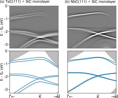
where = 1 indexes conduction and valence bands and = 1 the spin-split bands, is the band curvature while 2 and 2 are, respectively, the intrinsic spin-orbit splitting and extrinsic Bychkov-Rashba splitting. Good agreement with the experimental data is found using 2=60 meV and 2=160 meV, which at (i.e., ) corresponds to an absolute splitting in the valence bands of 220 meV. For reference, this is comparable to the largest reported band splittings observed in graphene following Au (100 meV Marchenko2012 ; Marchenko2016 ) or Pb intercalation (200 meV Klimovskikh2017 ). The sizable band splitting here derives from the heavy Ta atoms, readily confirmed by comparing with the same 2D-SiC termination that also forms on lighter niobium carbide films prepared in the same way (Figure 6)
The atomistic details of how this honeycomb SiC layer forms remain to be clarified. If we consider the SiC substrate in isolation, graphitization by thermal decomposition is a complex but by now well-understood phenomenonShtepliuk2016 . At temperatures of 1400℃ silicon atoms sublime from the surface while carbon, with a lower vapor pressure, does not. This leaves a carbon-rich layer that recrystallizes as graphene. In contrast, TaC is significantly more stable at high temperatures; to decompose it on a timescale of minutes would require extraordinary temperatures (3000℃Kempter1960 ) far from what has been reached here. Therefore we expect that the process is driven by the decomposition of the underlying SiC, leaving the TaC film intact. The most likely scenario is that the SiC termination forms during the post-deposition anneal of the TaC film to 1700℃, with Si and C diffusing through the TaC to accumulate on the surface. In this scenario, the sole function of the UHV annealing, at least for temperatures up to 1000℃, is to eliminate oxidation of the already-present SiC layer on the surface. This is consistent with our observation that the surface condition is unaffected by longer or additional UHV anneals. However, this does not hold for much higher UHV annealing temperatures (1200℃), for which the surface termination transforms into graphene (see Supplementary Material).
In conclusion, we have demonstrated a route to prepare large-area, high-quality SiC honeycomb monolayers through the annealing of thin films of transition metal carbides grown on 4H-SiC(0001). We have shown this for TaC and NbC, but anticipate that the process is generic and may also occur with other suitably lattice-matched rocksalt monocarbides on SiC such as VC, TiC, or WC. Band structure calculations provide good overall agreement with ARPES measurements. Together they reveal that the band of the SiC layer hybridizes with the underlying TaC surface states to yield a strongly spin-orbit split Dirac-like feature at the points. Beyond seeking a clearer understanding of the formation mechanism, in the future it will be interesting to explore possibilities of modifying this termination by intercalation or adsorption of other species. Such experiments may decouple the SiC layer from the substrate, alter the band splitting or even bring the Dirac-like feature towards the Fermi energy. The bottom-up fabrication technique shown here finally brings 2D SiC monolayers into the growing family of honeycomb structured monolayers.
Acknowledgements.
We thank D. Carbone for assistance during photoemission measurements and useful discussions. This work was jointly supported by the Swedish Foundation for Strategic Research (SSF) (No. GMT14-0077, No. RMA15-0024), Chalmers Excellence Initiative Nano, the Swedish Research council under Contract No. 2021-05252, 2D TECH VINNOVA competence Center (Ref. 2019-00068) and the Chalmers-MAX IV collaboration program. This work was performed in part at Myfab Chalmers. Research conducted at MAX IV, a Swedish national user facility, is supported by the Swedish Research council under Contract No. 2018-07152, the Swedish Governmental Agency for Innovation Systems under Contract No. 2018-04969, and Formas under Contract No. 2019-02496.References
- [1] P. Mélinon, and B. Masenelli and F. Tournus and A. Perez, Playing with carbon and silicon at the nanoscale, Nat. Mater. 6, 479 (2007)
- [2] H. Şahin, S. Cahangirov, M. Topsakal, E. Bekaroglu, E. Akturk, R. T. Senger, S. Ciraci, Monolayer honeycomb structures of group-IV elements and III-V binary compounds: First-principles calculations, Phys. Rev. B 80, 155453 (2009)
- [3] M. N. Huda, Y. Yan, M. M. Al-Jassim, On the existence of Si–C double bonded graphene-like layers, Chem. Phys. Lett. 479, 255 (2009)
- [4] L-J. Zhou, Y-F. Zhang, L-M. Wu, SiC2 Siligraphene and Nanotubes: Novel Donor Materials in Excitonic Solar Cells, Nano Lett. 13, 5431 (2013)
- [5] Z. Shi, Z. Zhang, A. Kutana, B. I. Yakobson, Predicting Two-Dimensional Silicon Carbide Monolayers, ACS Nano 9, 9802 (2015)
- [6] Z. Cui and Y. Qian and W. Zhang and H. Weng and Z. Fang, Type-II Dirac Semimetal State in a Superconductor Tantalum Carbide, Chin. Phys. Lett. 37, 087103 (2020)
- [7] D. Y. Yan and M. Yang and C. X. Wang and P. B. Song and C. J. Yi and Y. G. Shi, Superconductivity in centrosymmetric topological superconductor candidate TaC, Supercond. Sci. Technol. 34, 035025 (2021)
- [8] T. Shang, J. Z. Zhao, D. J. Gawryluk, M. Shi, M. Medarde, E. Pomjakushina, and T. Shiroka, Superconductivity and topological aspects of the rocksalt carbides NbC and TaC, Phys. Rev. B. 101, 214518 (2020)
- [9] L. Huder, G. Trambly de Laissardière, G. Lapertot, A.G.M. Jansen, C. Chapelier, V.T. Renard, Graphene on TaC: Air tight protection of a superconducting surface, Carbon 140, 592 (2018)
- [10] T. Le Quang, L. Huder, F. Lipp Bregolin, A. Artaud, H. Okuno, N. Mollard, S. Pouget, G. Lapertot, A.G.M. Jansen, F. Lefloch, E.F.C. Driessen, C. Chapelier, V.T. Renard, Epitaxial electrical contact to graphene on SiC, Carbon 121, 48 (2017)
- [11] S. Chabi and K. Kadel, Two-Dimensional Silicon Carbide: Emerging Direct Band Gap Semiconductor, Nanomaterial. Nanotechnol. 10, 2226 (2020)
- [12] T.-Y. Lü, X.-X. Liao, H.-Q. Wang and J.-C. Zheng, Tuning the indirect–direct band gap transition of SiC, GeC and SnC monolayer in a graphene-like honeycomb structure by strain engineering: a quasiparticle GW study, J. Mater. Chem. 22, 10062 (2012)
- [13] X. Lin, S. Lin, Y. Xu, A. A. Hakro, T. Hasan, B. Zhang, B. Yu, J. Luo, E. Li and H. Chen, Ab initio study of electronic and optical behavior of two-dimensional silicon carbide, J. Mater. Chem. C 1, 2131 (2013)
- [14] H. C. Hsueh, G. Y. Guo and S. G. Louie, Excitonic effects in the optical properties of a SiC sheet and nanotubes, Phys. Rev. B 84, 085404 (2011)
- [15] S. S. Lin, Light-Emitting Two-Dimensional Ultrathin Silicon Carbide, J. Phys. Chem. C 116, 3951 (2012)
- [16] T. Susi, V. Skákalová, A. Mittelberger, P. Kotrusz, M. Hulman, T. J. Pennycook, C. Mangler, J. Kotakoski and J. C. Meyer, Computational insights and the observation of SiC nanograin assembly: towards 2D silicon carbide, Sci. Rep. 7, 4399 (2017)
- [17] S. Chabi, Z. Guler, A. J. Brearley, A. D. Benavidez and T. S. Luk, The Creation of True Two-Dimensional Silicon Carbide, Nanomaterials 11, 1799 (2021)
- [18] L. E. Toth, Transition Metal Carbides and Nitrides (Academic Press, New York, 1971)
- [19] M. Stockmeier, R. Müller, S. A. Sakwe, P. J. Wellmann, and A. Magerl, On the lattice parameters of silicon carbide, J. Appl. Phys. 105, 033511 (2009)
- [20] See Supplementary Material for additional information about experimental methods, sample preparation and characterization and additional DFT calculations. That document includes references 21-23.
- [21] P. Giannozzi et al., Quantum Espresso: A modular and open-source software project for quantum simulations of materials, J.Phys. Condens. Matter 21, 395502 (2009)
- [22] P. Giannozzi et al., Advanced capabilities for materials modelling with Quantum Espresso, J.Phys. Condens. Matter 29, 465901 (2017)
- [23] T. Anazawa, S. Tokumitsu, R. Sekine, E. Miyazaki, K. Edamoto, H. Kato, S. Otani, Angle-resolved photoemission study of the surface electronic structure of TaC(111), Surf. Sci. 328, 263 (1995)
- [24] A. L. Giorgi, E. G. Szklarz, E. K. Storms, A. L. Bowman, and B. T. Matthias, Effect of Composition on the Superconducting Transition Temperature of Tantalum Carbide and Niobium Carbide, Phys. Rev. 125, 837 (1962)
- [25] L. I. Johansson, Electronic and structural properties of transition-metal carbide and nitride surfaces, Surf. Sci. Rep. 21, 177 (1995)
- [26] G. R. Gruzalski and D. M. Zehner, Defect states in sub-stoichiometric tantalum carbide, Phys. Rev. B 34, 3841 (1986)
- [27] Gmitra, M. and Konschuh, S. and Ertler, C. and Ambrosch-Draxl, C. and Fabian, J. Band-structure topologies of graphene: Spin-orbit coupling effects from first principles, Phys. Rev. B 80, 235431 (2009)
- [28] C. L. Kane and E. J. Mele, Quantum Spin Hall Effect in Graphene, Phys. Rev. Lett. 95, 226801 (2005)
- [29] D. Marchenko, A. Varykhalov, M. R. Scholz, G. Bihlmayer, E. I. Rashba, A. Rybkin, A. M. Shikin and O. Rader, Giant Rashba splitting in graphene due to hybridization with gold, Nat. Commun. 3, 1232 (2012)
- [30] D. Marchenko, A. Varykhalov, J. Sánchez-Barriga, Th. Seyller and O. Rader, Rashba splitting of 100meV in Au-intercalated graphene on SiC, Appl. Phys. Lett.108, 172405 (2016)
- [31] I. I. Klimovskikh, M. M. Otrokov, V. Yu Voroshnin, D. Sostina, L. Petaccia, Luca, G. Di Santo, S. Thakur, E. V. Chulkov and A. M. Shikin, Spin-Orbit Coupling Induced Gap in Graphene on Pt(111) with Intercalated Pb Monolayer, ACS Nano 11, 368 (2017)
- [32] I. Shtepliuk, V. Khranovskyy and R. Yakimova, Combining graphene with silicon carbide: synthesis and properties – a review, Semicond. Sci. Technol. 31, 113004 (2016)
- [33] C. P. Kempter and M. R. Nadler, Thermal Decomposition of Niobium and Tantalum Monocarbides, J. Chem. Phys. 32, 1477 (1960)