Bi layer properties in the Bi–FeNi
GMR-type structures
probed by spectroscopic ellipsometry
Abstract
Bismuth (Bi) having a large atomic number is characterized by the strong spin-orbit coupling (SOC) and is a parent compound of many 3D topological insulators (TIs). The ultrathin Bi films are supposed to be 2D TIs possessing the nontrivial topology, which opens the possibility of developing new efficient technologies in the field of spintronics. Here we aimed at studying the dielectric function properties of ultrathin Bi/FeNi periodic structures using spectroscopic ellipsometry. The [Bi()–FeNi(1.8 nm)]N GMR-type structures were grown by rf sputtering deposition on Sitall-glass (TiO2) substrates. The ellipsometric angles and were measured for the grown series (=0.6, 1.4, 2.0, 2.5 nm, N = 16) of the multilayered film samples at room temperature for four angles of incidence of 60∘, 65∘, 70∘, and 75∘ in a wide photon energy range of 0.5-6.5 eV. The measured ellipsometric angles, and , were simulated in the framework of the corresponding multilayer model. The complex (pseudo)dielectric function spectra of the Bi layer were extracted. The GMR effects relevant for the studied Bi–FeNi MLF systems are estimated from the optical conductivity zero-limit (optical GMR effect). The obtained results demonstrate that the Bi layer possesses the surface metallic conductivity induced by the SOC effects, which is strongly enhanced on vanishing the semimetallic-like phase contribution on decreasing the layer thickness, indicating its nontrivial 2D topology properties.
pacs:
Valid PACS appear hereI Introduction
The relativistic effect of spin–orbit (SOC) coupling is involved in the so-called Rashba effect Rashba . This phenomenon arises from the apparent loss of crystalline inversion symmetry near the surface or heterojunction leading to the lifting of the spin degeneracy and generating spin-polarized surface metallic states. In this respect, 3D (2D) topological insulators (TIs) also exhibit spin-polarized surface metallic states due to SOC. However, contrary to the Rashba effect, the surface metallic bands of a TI are determined by its bulk characteristics. The TIs host metallic surface states in a bulk energy gap, which are topologically protected. The surface (or interface) states of TIs can be topologically trivial or nontrivial. In the latter case, for example, electrons cannot be backscattered by impurities. Bismuth (Bi) having a large atomic number is characterized by the strong SOC and is a parent compound of many 3D TIs, such as Bi1-xSbx or Bi2Se3, even although 3D bulk Bi itself is topologically trivial. The specific feature of the electronic band structure of bulk Bi having rhombohedral symmetry Golin ; Gonze ; Liu1 is its inverted band gaps at both the and points of the Brillouin zone due to the strong SOC. The uniqueness of Bi films associated with the surface metallic states Hofmann ; Yokota and the semiconductor-to-metal transition Hoffman ; Koroteev are well documented in the literature.
Theoretical analyses predict a 1-bilayer (BL) Bi(111) film to be a 2D TI Wada ; Murakami . If there is no or weak inter-BL coupling, a stack of the odd-even 1-BL films will exhibit nontrivial to trivial oscillations of topology (where the topological number Kane is equal to 1 or 0, respectively). However, for the nontrivial topology in a stack of the 1-BL films, the intermediate inter-BL coupling strength, which is, for example, higher than the van der Waals strengths, is a mandatory condition. The direct ( point) and indirect band gap values were calculated by Liu et al. as a function of the Bi film thickness Liu2 . It was established that below 4BLs the film is a semiconductor with the direct gap open at the point and the positive indirect band gap leading to nontrivial topology peculiar for an intrinsic 2D TI. Above 4BLs the indirect band gap becomes negative resulting in a semiconductor- semimetal transition due to overlapping of two bands at the Fermi level around the and points. This suggests that the Bi films from 5 to 8 BLs represent a 2D TI situated between two trivial metallic surfaces Liu2 .
A comprehensive study of the associated SOC effects in ultrathin Bi layers opens the possibility of developing new efficient technologies in the field of spintronics. For this purpose, here we aimed at studying the dielectric function properties of ultrathin periodic structures Bi/Ni79Fe21, prepared by rf sputter deposition, which is one of the most common technologies used to grow coatings and multilayered films (MLFs) exhibiting a giant magnetoresistance (GMR) effect for various existing and modern nanotechnological applications. Earlier, we have demonstrated that electronic band structure and surface electronic properties of ultrathin Bi layers in real GMR-type (Bi–FeNi)N MLF structures incorporating nanoisland FeNi layers can be successfully studied by spectroscopic ellipsometry (SE) Kovaleva_APL_2021 . Here, by applying the elaborated SE approach, we investigate (Bi–FeNi) MLFs, where the thickness of the FeNi layer was 1.8 nm, corresponding to the FeNi layer structural percolation threshold Sherstnev ; Boltaev , and the Bi spacer layer was 0.6, 1.4, 2.0, and 2.5 nm thick, incorporating about 2, 4, 6, and 8 Bi-type planes, respectively. We found that the Bi spacer layers have the metallic surface conductivity, which demonstrates strongly enhanced metallicity properties on vanishing the Bi semimetallic-like phase contribution on decreasing the layer thickness, which can be constructive in finding new nontrivial 2D topology properties of the (Bi–FeNi) GMR-type structures for their different nanotechnological applications.
II Materials and Methods
The (Bi–FeNi)N MLFs were prepared in a sputter deposition system by cathode sputtering from 99.95% pure Bi and Fe21Ni79 targets in an alternative way. The base pressure in a sputter deposition chamber was 210-6 Torr. The multilayers were deposited at approximately 80 ∘C in an argon atmosphere of 6 10-4 Torr on to insulating glassy Sitall (TiO2) substrates. We utilized the substrates having typical dimensions 15 5 0.6 mm3. The nominal thicknesses of the FeNi and Bi layers were controlled by the layer deposition times in accordance with the material deposition rates. A series consisting of four MLF samples was prepared. In the series of the grown (Bi–FeNi)N samples, the nominal thickness of the FeNi layer was 1.8 nm and the Bi layer thickness was of 0.6, 1.4, 2.0, and 2.5 nm, the number N of the periodically repeated Bi/FeNi layers was 16. The thickness of the FeNi layer was chosen to be 1.8 nm matching the structural percolation threshold Sherstnev ; Boltaev . The Bi layer thicknesses were chosen in such a way that the conditions for ferromagnetic (FM) or antiFM coupling in the GMR-type structures would be optimized. To prevent degradation, the deposited (Bi–FeNi)16/Sitall samples were covered with the 2.1 nm-thick Al2O3 layer.
The related [Bi–FeNi(0.8,1.2 nm)]N samples prepared by rf sputtering deposition onto the Sitall substrates under similar conditions were investigated by X-ray diffraction (XRD) as well as by X-ray reflectivity (XRR) experimental techniques in our previous study (see Supplementary online information for the article Kovaleva_APL_2021 ). The XRR spectra proved a good periodicity and consistency with the corresponding nominal thicknesses of the FeNi and Bi slices in the Bi/FeNi MLF structures, as well as relatively low interface roughness between the constituent layers. The XRD characterization suggests (012)-type Bi plane orientation, where the interlayer distance is 3.28 Å. It follows from this that in the studied MLF structures the Bi layers with a thickness corresponding to 0.6, 1.4, 2.0, and 2.5 nm incorporate two, four, six, and eight Bi(012)-type planes, respectively.
In the present study, the surface morphology of the Bi–FeNi(1.8 nm) MLF samples, prepared by rf sputtering deposition on the Sitall (TiO2) substrates, was studied at room temperature using an ambient AFM (Bruker, Dimension Icon) in the Peak Force Tapping mode with ScanAsyst Air tips (Bruker, k=0.4 N/m, nominal tip radius 2 nm). The SE measurements for the investigated Al2O3/(Bi–FeNi)16/Sitall samples were performed at room temperature in a wide photon energy range of 0.5 – 6.5 eV using a J.A. Woollam VUV-VASE ellipsometer (see the scheme illustrating the SE study of the (Bi–FeNi)N MLFs in Fig. 1(a) of Ref. Kovaleva_APL_2021 ). The measured ellipsometry spectra are represented by real values of the angles and , which are defined through the complex Fresnel reflection coefficients for light-polarized parallel and perpendicular to the plane of incidence, . The ellipsometric angles, and , measured for the Bi–FeNi MLF samples were simulated using the multilayer model simulation available in the J.A. Woollam VASE software VASE . From the multilayer model simulations, the (pseudo)dielectric function spectra of the ultrathin 0.6, 1.4, 2.0, and 2.5 nm Bi layers and 1.8 nm FeNi layer inside the Bi–FeNi MLF structures were extracted. The corresponding calculated optical conductivity spectra were analyzed.
III Results
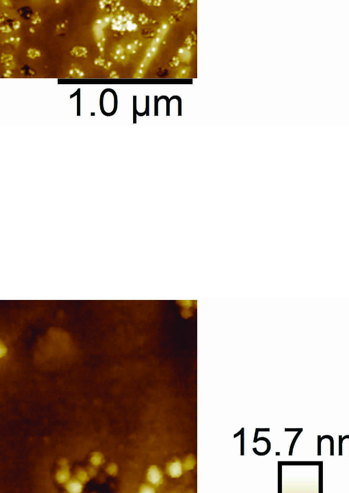
III.1 Atomic force microscopy study
The retrieved 55 m2 and 11 m2 AFM images of the Al2O3(2.1 nm)/[Bi(0.6, 1.4, 2.0, 2.5 nm)–FeNi(1.8 nm)]N/Sitall multilayered films (where the given layer thicknesses correspond to their nominal values), presented in Figure 1a–h show discernable contrast because of the available surface hight deviations. The surface roughness of the Sitall glass (TiO2) substrates was investigated by us by AFM in our earlier publication Stupakov . The height profile of the Sitall substrates (see Fig. 2a of Ref. Stupakov ) demonstrated the height deviation within the range 1-3 nm peculiar to the relatively large 0.3-1 m lateral scale, which characterizes the Sitall substrate surface roughness. From the AFM measurements on the areas 55 m2 and 11 m2 the root-mean square (RMS) surface roughness values were evaluated, which are presented in the caption to Figure 1. The corresponding RMS roughness values are notably higher for the Al2O3(2.1 nm)/[Bi(2.5 nm)–FeNi(1.8 nm)]16/Sitall MLF sample. The smaller-scale (1 1 m2) images clearly recognize a fine grainy-like structure of the surface morphology, which seems to be characteristic for all studied film samples (see Figure 1e–h). The typical grain size, being of about 50 nm, is notably larger for the FeNi(1.8 nm) – Bi MLF sample incorporating the 2.5 nm-thick Bi layers, and, following the estimated RMS roughness values, the average grain size decreases to about 20 nm with decreasing the Bi layer thickness to 1.4 nm. As one can see from the typical height profiles presented in Figure 1i,j, with decreasing the Bi layer thickness from 2.5 to about 0.6 nm, the surface morphology becomes highly irregular due to the formation of conglomerates of nanoislands separated by rather flat (relatively small roughness) areas of about 20 nm.
III.2 Spectroscopic ellipsometry study of the ultrathin Bi–FeNi multilayer film samples
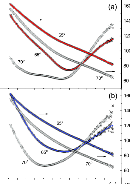
The ellipsometric angles and were measured for the prepared Al2O3/(Bi–FeNi)16/Sitall MLF samples at the angles of incidence of 60∘, 65∘, 70∘, and 75∘. Figure 2 demonstrates the ellipsometric angles and recorded at 65∘ and 70∘. To model the contributions from free charge carriers and interband optical transitions, the complex dielectric function of the Bi and FeNi layers was interpreted in terms of the Drude and Lorentz parts, respectively,
| (1) |
where is the high-frequency dielectric constant, which takes into account the contribution from the higher-energy interband transitions. The fitted Drude parameters were and free charge carrier’s scattering rate . The fitted parameters of Lorentz bands were , , and of the band maximum energy, the full width at half maximum, and the band height, respectively. The obtained ellipsometric angles and measured at different angles of incidence of 60∘, 65∘, 70∘, and 75∘ were fitted for each sample simultaneously using the J.A. Woollam VASE software VASE in the framework of the designed multilayer model. The multilayer model for the studied Al2O3/(Bi–FeNi)/Sitall multiayers was constructed as it is schematically presented in Figure 3, exactly so as the layers were deposited. In addition, we attempted to take into account the roughness properties of the surface by using the conventional approach of effective medium approximation (EMA) based on the (50% Al2O3–50% vacuum) Bruggeman model. The dispersion model for the Bi layers included three or four Lorentz terms as well as the Drude part. The dispersion model for the 1.8 nm permalloy layers incorporated in the studied MLF structures included the Drude term responsible for the free charge carrier contribution and one Lorentz oscillator to account for the most pronounced interband optical transition. In addition, the dielectric function spectra of the bare Sitall substrate derived from our earlier SE studies Kovaleva_APL_2015 ; Kovaleva_metals were introduced to the elaborated multilayer model. The dielectric response of the Al2O3 capping layer was represented by the tabular complex dielectric function spectra Palik . The thicknesses of the Bi and FeNi layers, as well as of the surface layers, were fitted. The unknown parameters were allowed to vary until the minimum of the mean squared error (MSE) is reached. The best simulation result for the studied [Bi(0.6, 1.4, 2.0, 2.5 nm)–FeNi(1.8 nm)]16 MLF samples corresponded to the lowest obtained MSE values of 0.3843, 0.297, 0.2934, and 0.4508, respectively. The good quality of the fit allowed us to estimate the actual Bi and FeNi layer thicknesses in the MLFs under study. The quality of the fit is demonstrated by Figure 2, where we plotted the measured ellipsometric angles along with the simulation results. The Drude and Lorentz parameters resulting from the simulation of the Al2O3/[Bi()–FeNi(1.8 nm)]16/Sitall MLF samples are given in Tables 1 and 2, and the resulting and parts of the Bi and FeNi (pseudo)dielectric function spectra are presented in Figure 4.
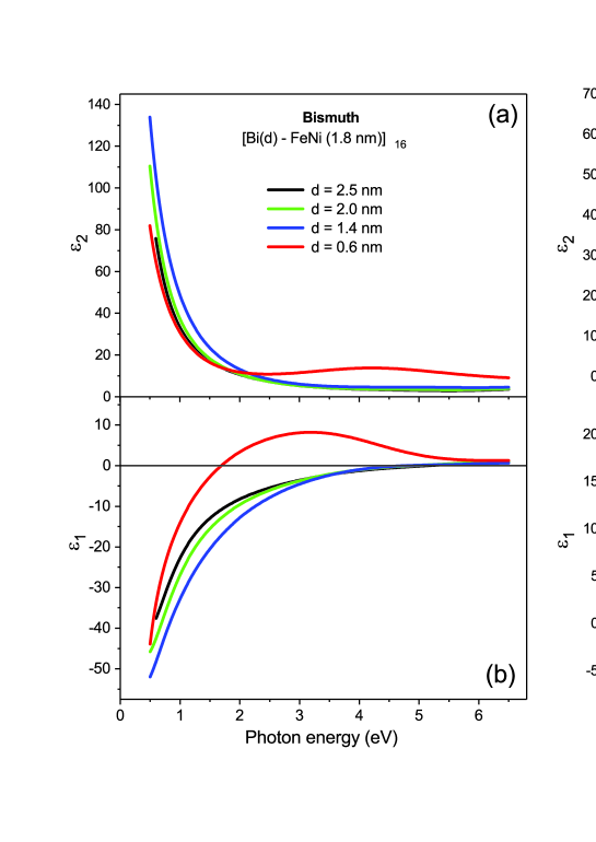
From Figure 4a,b one can see that the complex (pseudo)dielectric functions of the 0.6, 1.4, 2.0, and 2.5 nm thick Bi spacers inside the investigated Bi–FeNi MLFs demonstrate metallic character. Moreover, the function progressively decreases while the Bi thickness decreases from 2.5–2.0 to 1.4 nm and the increases at low photon energies, respectively. According to our simulation results, we expect that the best metallicity properties are demonstrated by the Bi layer in the [Bi(1.4 nm)–NiFe(1.8 nm)]16 structure. At the same time, the complex (pseudo)dielectric functions of the thinnest 0.6 nm thick Bi layer look somewhat different. Here, in addition to the low-energy metallic Drude response identified by the characteristic behavior of the and , the Lorentz band around 4–5 eV makes an essential contribution to the dielectric function response (the corresponding Drude ( and ) and Lorentz (, , and ) parameters are listed in Table 1). Next, being similar, the dielectric functions of the 1.8 nm thick permalloy layers in the [FeNi–Bi(1.4, 2.0, 2.5 nm)] MLFs are dominated by the resonance and antiresonance features, indicating the predominant contribution from the Lorentz oscillator peaking at around 3 eV (see Figure 4c,d). An upturn evident in the at low photon energies indicates an additional Drude contribution, which is relatively less pronounced. Following our simulation results, we expect the advanced metallicity properties of the FeNi layer in the [Bi(0.6 nm)–NiFe(1.8 nm)]16 structure (see the corresponding Drude ( and ) and Lorentz (, , and ) parameters listed in Table 2).
| Parameters | 0.6 nm | 1.4 nm | 2.0 nm | 2.5 nm | |
|---|---|---|---|---|---|
| Drude | 46.(9)4 | 66.(7)4 | 24.(5)4 | 25.(1)2 | |
| 1.2(5)0.09 | 1.51(0)0.06 | 2.7(2)0.4 | 3.1(3)0.2 | ||
| 6300540 | 8970540 | 3290540 | 3370270 | ||
| Lorentz | – | 0.45(8)0.05 | 0.35(9)0.01 | 0.38(6)0.004 | |
| oscillator | – | 15.(0)6 | 96.(0) | 70.(8)2 | |
| – | 0.52(6)0.09 | 0.79(1)0.02 | 0.67(6) | ||
| Lorentz | 4.67 | 5.31(5)0.03 | 5.08(7)0.04 | 4.77(5)0.04 | |
| oscillator | 10.2(7)0.6 | 2.53(2)0.05 | 1.2(5)0.1 | 0.67(6)0.08 | |
| 4.2(1)0.07 | 3.99(3)0.07 | 3.4(7)0.2 | 2.5(5)0.2 | ||
| Lorentz | 11.1 | 7.8 | 7.7 | 7.7 | |
| oscillator | 7.2 | 4.1 | 4.1 | 4.1 | |
| 8.9 | 2.8 | 2.8 | 2.8 |
| Parameters | 0.6 nm | 1.4 nm | 2.0 nm | 2.5 nm | |
|---|---|---|---|---|---|
| Drude | 33.(8)2 | 15.(0)1 | 21.(7)2 | 13.(1)2 | |
| 0.876(5)0.04 | 2.8(2)0.3 | 3.4(2)0.4 | 3.1(3)0.2 | ||
| 4540270 | 2020130 | 2920270 | 1760270 | ||
| Lorentz | 1.87 | 3.32 | 3.32 | 3.32 | |
| oscillator | 14.76 | 14.28 | 15.23 | 14.74 | |
| 3.62 | 5.88 | 5.65 | 5.95 |
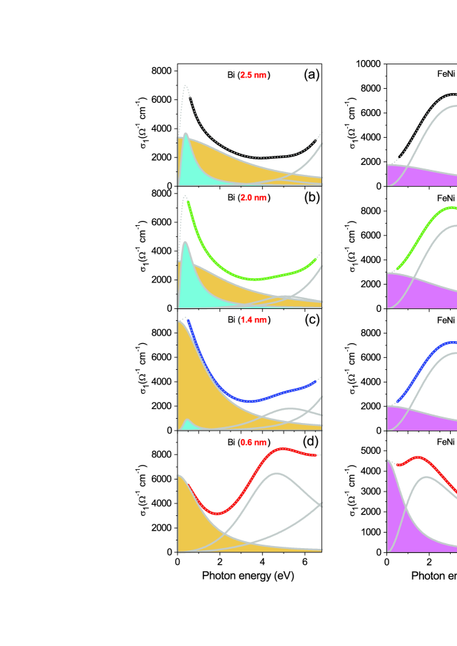
Figure 5a–d presents the evolution of the Bi intralayer optical conductivity, (cm-1)/60, upon decreasing the Bi spacer layer thickness in the [FeNi(1.8 nm) – Bi(2.5, 2.0, 1.4, 0.6 nm)]16 structures, and Figure 5e–h shows the associated optical conductivity spectra of the 1.8 nm FeNi permalloy layer. Here, the contributions from the Drude and Lorentz oscillators following the multilayer model simulations using Equation 1 are evidently demonstrated. The optical conductivity spectra of the Bi and FeNi layers follow the main trends identified in their complex dielectric function spectra presented in Figure 4.
IV Discussion
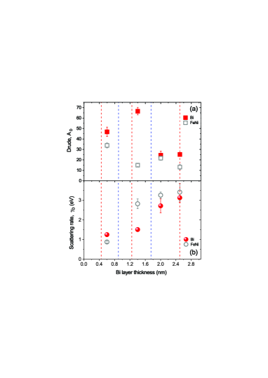
Initially, we would like to discuss GMR effects relevant for the studied MLF systems. Our simulations of the dielectric functions for the 1.8 nm-thick NiFe layer inside the [Bi(0.6,1.4,2.0,2.5 nm)–NiFe(1.8 nm)] MLFs show the presence of the Drude term complemented with the pronounced Lorentz band located at around 2–3 eV (see Table 2). From the corresponding optical conductivity spectra presented in Figure 5e–h one can notice that the associated Drude dc limit, , displays an oscillating character (in agreement with the results deduced for the corresponding Drude parameter , see Table 2 and Figure 6). We can expect that the Bi spacer thicknesses for which the FeNi layers are preferentially antiFM coupled in the studied MLFs are around 1.4 and 2.5 nm implying that the [Bi(1.4,2.5 nm)–NiFe(1.8 nm)]16 film structures will exhibit a drop in the resistance (being negative magnetoresistance) when exposed to an external magnetic field. It is well known from the literature that the first antiFM maximum exhibits negative magnetoresistance of about 20%, while the second antiFM maximum decreases to about 10%, and the presence of the third antiFM maximum cannot confidently be retrieved (see, for example, Ref. Huetten and references therein). Using a simple model of a two-current series resistor Mathon , the magnetoresistance can be estimated as
| (2) |
where and are the thicknesses of Bi and FeNi layers, and and are the ratios of the resistivity in the FeNi layer to that in the Bi layer in the spin down and spin up current channel, respectively. Exploiting values for estimated for the 1.4 nm Bi and 1.8 nm FeNi layers from the current model simulations (see Table 1 and 2), namely, =cm, =cm and =cm (the latter estimate is given by the FM coupling for the 0.6 nm Bi spacer), we obtain =4.4 and =2.0. Then, using Equation (2) we have =10%. This means that the 1.4 nm Bi spacer corresponds to the second antiFM maximum. Following the same approach for the 2.5 nm Bi spacer, where =cm, =cm and =cm (corresponding to the FM coupling for the 2.0 nm Bi spacer), we obtain =1.9 and =1.2. Using Equation (2), we have =1.4%, which may correspond to the very weakly pronounced third antiFM maximum. From the analysis presented above, we may expect that the first antiFM maximum corresponding to the magnetoresistance of about 20% occurs for the Bi spacer thickness of about 0.9 nm, which is in agreement with the results presented in Ref. Huetten .
Further, in the XRD patterns of the investigated Al2O3/[Bi(1.4,2.0,2.5 nm)–NiFe(1.8 nm)]16/Sitall film samples, the peak of the crystalline Bi phase is identified at 2 26.2∘ suggesting orientation of the Bi layers, which is characterized by the interlayer distance of 3.28 Å. Using STM and reflection high-energy electron diffraction (RHEED) techniques, it was shown that initial growth of Bi-type films occurs in the form of islands with the height increment of about 6.6 Å, indicating even-number layer stability leading to the laterally flat morphology of the Bi-type islands Nagao . Consequently, we can expect that the 0.6, 1.4, 2.0, and 2.5 nm Bi spacer layers in the investigated MLFs incorporate about 2, 4, 6, and 8 -type Bi planes, respectively.
The model simulations for the [Bi(2.5, 2.0 nm)–FeNi(1.8 nm)]16 film samples reveal that the low-energy dielectric function of the Bi intralayers has competing contributions from the Drude term and from the intense Lorentz band around 0.36–0.39 eV with a maximum height of 70–100 (see Table 1). The Drude and Lorentz contributions are more clearly pronounced in the corresponding optical conductivity spectra (see Figure 5a,b). The obtained Drude and Lorentz parameters are in excellent agreement with those deduced in our previous study Kovaleva_APL_2021 for the Bi spacer layer incorporated in the [Bi(2.5, 2.0 nm)–NiFe(1.2 nm)]16 structures under study. The pronounced Lorentz band found at low photon energies for Bi single crystals (rhombohedral symmetry, space group ) Wang ; Lenham and bulk Bi layers Hunderi ; Toudert is characteristic of the semimetallic-like electronic band structure due to the contributions from the interband transitions near the point, – and – Golin , and near the T point, T – T Liu1 . The estimated values (see Table 1) of the Drude dc limit (2750–3830 cm-1) as well as the free charge carrier’s (2.3–3.3 eV) are consistent with those peculiar for the metallic surface states related to the Rashba SOC in Bi(111) films, = 2300 cm-1 and = 2.0 eV) Yokota . Meanwhile, the model simulation for the [Bi(1.4 nm)–NiFe(1.8 nm)]16 structure indicates that for the 1.4 nm Bi layer the Drude dc limit significantly increases to 8970540 cm-1, while the essentially decreases to 1.500.06 eV. In this case, the Lorentz band is nearly suppressed. The associated found Drude parameters for the ultrathin Bi layer inside the [Bi(0.6 nm)–NiFe(1.8 nm)]16 structure are slightly different, namely, = 6300540 cm-1 and = 1.20.1 eV, and the Lorentz band is not present clearly (see Figure 5c,d and Table 1).
Thus, we have discovered that, on the one hand, the optical conductivity spectra spectra of the 2.0 and 2.5 nm thick Bi spacer layers in the (Bi–FeNi) MLFs incorporating 8 and 6 Bi-type monolayers, respectively, have contributions from the pronounced low-energy Lorentz oscillator and from the free charge carrier Drude term (for details, see Figure 5a,b and Table 1). Here, the presence of the low-energy Lorentz band points on the Bi semimetallic phase contribution, and the parameters obtained for the Drude conductivity indicate that its origin can be associated with the surface metallic states Yokota . Therefore, the 2.0 and 2.5 nm Bi layers can be associated with the semimetallic Bi phase sandwiched between two metallic layers on the top and bottom surfaces. On the other hand, the contribution from the intrinsic Lorentz band is strongly suppressed for the 1.4 and 0.6 nm layers, where the Drude conductivity displays notably improved metallicity properties, as one can see from the optical conductivity spectra shown in Figure 5c,d (for details, see Table 1).
From the above discussion of the obtained results, we can conclude that the Bi layer consisting of 4 Bi(012)-type monolayers represents a kind of crossover regarding the contributions from the semimetallic Bi phase and/or surface metallic-like states. Here we noticed some similarity with the theory results presented for the ultrathin Bi(111) layers by Liu et al. Liu2 . There, it was established that below 4 Bi(111) BLs the film is a semiconductor with the direct gap open at the point and the positive indirect band gap, leading to nontrivial topology (=1) peculiar for an intrinsic 2D TI. Hovewer, above 4 Bi(111) BLs, the indirect band gap becomes negative resulting in a semiconductor-semimetal transition due to overlapping of two bands at the Fermi level around the and points. It is argued by Liu et al. Liu2 that the Bi layers consisting of 5 to 8 Bi(111) BLs represent a 2D TI suited between two “trivial” metallic surfaces Liu2 . This means that for the surface considered as an individual 2D system its number is trivial (=0). The surface bands have no contribution to the nontrivial topology and, therefore, these trivial metallic surfaces are not robust and can easily be removed by surface defects or impurities. It was found by us Kovaleva_APL_2021 that the Bi layers in the [Bi(2.0, 2.5 nm)–NiFe(0.8 nm)] multilayers, incorporating the nanoisland permalloy layer, exhibit bulk-like semimetallic properties of the electronic band structure, although the surface (Drude) metallic conductivity is absent there (see Fig. 4(d) of Ref. Kovaleva_APL_2021 ). Indeed, strong magnetic and spatial disorder induced by magnetic FeNi nanoislands, as well as long-range many-body interactions between magnetic moments of permalloy nanoislands Stupakov , may lead to specific localization of free charge carriers Kovaleva_SciRep . However, the surface conductivity (or interface) states for the 1.4 nm layer in the Bi–FeNi(1.8 nm) multilayers may be topologically nontrivial and, in this case, the electrons cannot be backscattered by impurities. Here, the Drude dc limit is 8970540 cm-1 and the scattering rate =1.50.06 eV. We found that the 0.6 nm thick Bi layer exhibits somewhat different Drude dc limit (6300540 cm-1) and (1.20.1 eV), see Table 1 and Figure 6, which can be attributed to the discontinuous nanoisland structure of this layer.
Finally, we would like to note that it will be challenging to investigate dc transport and superconductivity properties of the ultrathin Bi films possessing 2D TI surface states following the approach presented in Ref. Suslov , where the subkelvin superconductivity without any external stimuli was discovered in 3D TI Cd3As2 films Kochura ; Kovaleva_metals_2020 .
V Conclusions
In summary, using wide-band (0.5-6.5 eV) spectroscopic ellipsometry we
studied the optical properies of the
[Bi(0.6, 1.4, 2.0, 2.5 nm)–NiFe(1.8ṅm)]16 MLFs
prepared by rf sputtering.
The XRD analysis suggested that the 0.6, 1.4, 2.0, and 2.5 nm Bi layers in the studied MLFs correspond to about two, four, six, and eight
Bi-type monolayers, respectively. From the multilayer model simulations of the measured ellipsometric data, we extracted the Bi and FeNi layer dielectric functions. The dielectric function for the 2.0 and 2.5 nm Bi spacer layers are represented by the Drude resonance due to the surface states and the low-energy Lorentz band peaking at around 0.3-0.4 eV. The pronounced Lorentz band is characteristic of the semimetallic bulk-like Bi electronic zone structure due to the contributions from the interband transitions near the point. We discovered that the 2.0 and 2.5 nm Bi spacer layers can be associated with the semimetallic Bi phase sandwiched between two trivial (where the topology number =0) metallic layers on the top and bottom surfaces. The contribution from the low-photon-energy Lorentz band is strongly suppressed for the 1.4 and 0.6 nm Bi layers, where the Drude conductivity displays notably improved metallicity properties. This indicates that the Bi layer consisting of 4 Bi-type monolayers represents a kind of crossover regarding the contributions from the semimetallic Bi phase and/or surface metallic-like states. Therefore, the properties of Bi layers below 4 monolayers may be associated with nontrivial topology (where the topology number =1) peculiar for an intrinsic 2D TI.
We expect that the Bi layers having thickness of 0.9 nm will exhibit maximal GMR effect of about 20% in the (Bi-FeNi) MLFs, where the Drude dc limit is about 8970540 cm-1. These states may be protected from backscattering, which makes them promising in spintronic devices and quantum computing.
Acknowledgement
We thank F.A. Pudonin for providing us with the
Bi/FeNi multilayer film samples and O. Pacherova for their
XRD analysis. We thank A. Muratov for participation in the spectroscopic ellipsometry measurements. This work was supported by the European Structural and Investment Funds and the Czech Ministry of Education, Youth, and Sports (Project No. SOLID21, Cz.02.1.01/0.0/0.0/16-019/0000760).
Declaration of competing interest
The authors declare no conflict of interest.
References
- (1) Bychkov, Y.A.; Rashba, E.I. JETP Lett., 1984, 39, 78.
- (2) Golin, S. Phys. Rev. B, 1968, 166, 643.
- (3) Gonze, X.; Michenaud, J.-P.; Vigneron, J.-P. Phys. Rev. B, 1990, 41, 11827.
- (4) Liu, Y.; Allen, R.E. Phys. Rev. B, 1995, 52, 1566.
- (5) Hofmann, Ph. Prog. Surf. Sci., 2006, 81, 191.
- (6) Yokota, Y.; Takeda, J.; Dang, C.; Han, G.; McCarthy, D.N.; Nagao, T.; Hishita, S.; Kitajima, K.; Katayama, I. Appl.Phys. Lett., 2012, 100, 251605.
- (7) Hoffman, C.A.; Meyer, J.R.; Bartoli, F.J. Phys. Rev. B, 1993, 48, 11431.
- (8) Koroteev, Yu. M.; Bihlmayer, G.; Chulkov, E.V.; Blugel, S. Phys. Rev. B, 2008, 77, 045428.
- (9) Wada, M.; Murakami, S.; Freimuth, F.; Bihlmayer, G. Phys.Rev.B, 2011, 83, 121310(R).
- (10) Murakami, S. Phys. Rev. Lett., 2006, 97, 236805.
- (11) Fu, L.; Kane, C.L.; Mele, E.J. Phys. Rev. Lett., 2007, 98, 106803.
- (12) Liu, Z.; Liu, C.-X.; Wu, Y.-S.; Duan, W.-H.; Liu, F.; Wu, J. Phys. Rev. Lett., 2011, 107, 136805.
- (13) Kovaleva, N.N.; Chvostova, D.; Pacherova O.; Muratov A.V.; Fekete L.; Sherstnev I.A.; Kugel K.I.; Pudonin F.A.; Dejneka A. Appl. Phys. Lett., 2021, 119, 183101.
- (14) Sherstnev, I.A. Ph. D. Thesis; P.N. Lebedev Physical Institute: Moscow, Russia, 2014.
- (15) Boltaev, A.P.; Pudonin, F.A.; Shertnev, I.A.; Egorov, D.A. JETP, 2017, 125, 465.
- (16) Woollam, J.A. VASE Spectroscopic Ellipsometry Data Analysis Software; J.A. Woollam, Co.: Lincoln, NE, 2010.
- (17) Stupakov, A.; Bagdinov, A.V.; Prokhorov, V.V.; Bagdinova, A.N.; Demikhov, E.I.; Dejneka, A.; Kugel, K.I.; Gorbatsevich, A.A.; Pudonin, F.A.; Kovaleva, N.N. J. Nanomater., 2016, Article ID 3190260.
- (18) Kovaleva, N.N.; Chvostova, D.; Bagdinov, A.V.; Petrova M.G.; Demikhov E.I.; Pudonin F.A.; Dejneka A. Appl. Phys. Lett., 2015, 106, 051907.
- (19) Kovaleva, N.; Chvostova, D.; Dejneka, A. Metals, 2017, 7, 257.
- (20) Palik, E.D. Handbook of Optical Constants of Solids; Elsevier Science: USA, 1991.
- (21) Hütten, A.; Mrozek, S.; Heitmann, S.; Hempel, T.; Brückl H.; Reiss, G. Acta mater., 1999, 47, 4245.
- (22) Mathon, J. Contemporary Physics, 1991, 32, 143.
- (23) Nagao, T.; Sadowski, J.T.; Saito, M.; Yaginuma, S.; Fujikawa, Y.; Kogure, T.; Ohno, T.; Hasegawa, S.; Sakurai, T. Phys. Rev. Lett., 2004, 93, 105501.
- (24) Wang, P.Y.; Jain, A.L. Phys. Rev. B, 1970, 2, 2978.
- (25) Lenham, A.P.; Treherne, D.M.; Metcalfe, R.J. J. Opt. Soc. Am., 1965, 55, 1072.
- (26) Hunderi, O. J. Phys. F, 1975, 5, 2214.
- (27) Toudert, J.; Serna, R. Opt. Mater. Express, 2017, 7, 2299.
- (28) Kovaleva, N.N.; Kusmartsev, F.V.; Mekhiya, A.B.; Trunkin, I.N.; Chvostova, D.; Davydov, A.B.; Oveshnikov, L.N.; Pacherova, O.; Sherstnev, I.A.; Kusmartseva, A.; Kugel, K.I.; Dejneka, A.; Pudonin, F.A.; Luo,Y.; Aronzon, B.A. Sci. Rep. , 2020, 10, 21172.
- (29) Suslov, A.V.; Davydov, A.B.; Oveshnikov, L.N.; Morgun, L.A.; Kugel, K.I.; Zakhvalinskii, V.S.; Pilyuk, E.A.; Kochura, A.V.; Kuzmenko, A.P.; Pudalov, V.M.; Aronzon, B.A. Phys. Rev. B, 2019, 99, 094512.
- (30) Kochura, A.V.; Zakhvalinskii, V.S.; Htet, A.Z.; Ril’, A.I.; Pilyuk, E.A.; Kuz’menko, A.P.; Aronzon, B.A.; Marenkin, S.F. Inorg. Mater., 2019, 55, 879.
- (31) Kovaleva, N.; Chvostova, D.; Fekete, L.; Muratov, A. Metals, 2020, 10, 1398.