Renormalizing Antiferroelectric Nanostripes in via Optomechanics
Abstract
Antiferroelectric (AFE) materials have received tremendous attention owing to their high energy conversion efficiency and good tunability. Recently, an exotic two-dimensional (2D) AFE material, monolayer that could host atomically thin AFE nanostripe domains has been experimentally synthesized and theoretically examined. In this work, we apply first-principles calculations and theoretical estimations to predict that light irradiation can control the nanostripe width of such a system. We suggest that an intermediate near-infrared light (below bandgap) could effectively harness the thermodynamic Gibbs free energy, and the AFE nanostripe width will gradually reduce. We also propose to use an above bandgap linearly polarized light to generate AFE nanostripe-specific photocurrent, providing an all-optical pump-probe setup for such AFE nanostripe width phase transitions.
TOC Graphic
![[Uncaptioned image]](/html/2301.01425/assets/figures/TOC.png)
Ferroelectric (FE) materials, characterized by reversible spontaneous polarizations () and multi-domains, have been widely studied and extensively explored for electronic devices, such as non-volatile information storage elements 1 and field-effect transistors 2 over the past few decades. The miniaturization requirements for large data storage density urge to reduce the ferroelectric materials into sub-nanometer (or atomic) scales. This has been, over a long time, believed to be unrealistic due to strong depolarization field effect 3. Only until recently, scientists have theoretically predicted and experimentally demonstrated that low-dimensional (such as two-dimensional, 2D) intrinsic ferroelectric materials with nonvanishing and reversible dipole moments could exist in nature, e.g., group-IV monochalcogenide monolayers 4, 5, 6, 7, 8, 9, 10, 11, 12, 13, 14, 15, -transition-metal dichalcogenide monolayers16, 17, and 2D perovskites 18, 19, 20, 21, to name a few.
In addition to FEs, antiferroelectric (AFE) materials have also been attracting tremendous attention. Unlike FEs, the AFEs are immune to small external bias and exhibit a double electric-polarization hysteresis loop, which guarantees its high energy storage efficiency and large saturation polarization. Hence, AFE materials are also found to be promising for capacitors 22, 23, memristors24, 25, and piezoelectric11 applications. Compared with traditional bulk systems, 2D AFE systems are scarce, and more investigations remain largely under-explored. Recently, Xu et al. 26 performed a seminal theoretically and experimentally combined work and disclosed a promising 2D AFE phase, . Among the multiple phases in the polymorphic , the and phases could form 2D van der Waals (vdW) layers under room temperature ( phase appears under high temperature 27). These vdW layers consist of five atomic quintuple layers (Se-In-Se-In-Se), and they both belong to hexagonal lattice. Their difference lies at the atomically stacking patterns: The phase forms A-B-B-C-A stacking sequence, while the (and ) phase shows a merely A-B-C-A-B (fcc) order. Note that previous works have demonstrated that the precise fcc stacking sequence is dynamically unstable, and a shuffle of Se atom in the central atomic Se layer along could remove its soft phonon mode 12, 26. In this regard, an in-plane FE order appears (denoted as in this work). According to recent experimental observations 26, 28, this FE structure easily subjects to a phase transition and forms a -AFE pattern (denoted as here) with periodic antiparallel nanostripes, each of which contains a few unit cells. Unlike in conventional 3D bulk (anti-)ferroelectric materials that consist micro-sized multi-domains along various directions, the AFE nanostripes in are exotic as they are in-plane dominant and in the atomic scale order. Hence, it could yield ultrahigh density information storage and facile manipulations in a subtle precision, meeting the requirements for sub-nanometer field-effect transistors and information storage devices in the near future. Yet, the modulation of the nanostripe patterns requires further evaluation and careful investigations. Due to the zero net electric polarization nature in the AFEs, traditional electric bias strategy is not straightforwardly appropriate.
In this Letter, we propose that light-induced phase transition could occur in such AFE nanotripes, and the FE nanostripe width can be effectively manipulated. We illustrate this by performing first-principles density functional theory (DFT) calculations combined with optomechanical thermodynamic theory. Our results suggest that the nanostripe width of quintuple layer (QL) well-controls their relative stability. The optimal nanostripe width contains three unit cells at low temperature. Wider and narrower nanostripe AFE structures are slightly higher in total energy. Through a simple model, we propose how the AFE nanostripe interactions and the formation of domain walls control their internal energy. By systematically evaluating and comparing the electronic structures and electron contributed optical responses of these AFE systems, we reveal obvious optical contrasts in the near-infrared optical wavelength regime. Hence, under light illumination, we suggest that different optomechanical effect would occur, and one can realize a series of light-induced phase transitions to renormalize the FE nanostripe widths in the . This suggests a noncontacting and noninvasive phase transition strategy which, to the best of our knowledge, have not been disclosed in AFE materials. In addition, we predict that such nanostripe variations can be detected by the AFE nanostripe dependent bulk photovoltaic (BPV) effect under above bandgap light illumination. Through evaluating the BPV photocurrent for each nanostripe, we show that opposite flowing photocurrents exist along the nanostripe direction.
We perform DFT 29, 30 calculations within the Vienna ab initio simulation package (VASP) 31, 32. The exchange-correlation term in the Kohn-Sham equation is treated by the generalized gradient approximation (GGA) in the Perdew-Burke-Ernzerhof (PBE) form 33. Projector augmented-wave (PAW) method 34 and a planewave basis set are used to describe the core and valence electrons, respectively, which yield a computational accuracy comparable to all-electron calculations. The kinetic energy cutoff is set to be , and the -mesh separation in the first Brillouin zone (BZ) is set to be less than for each simulation supercell. The convergence criteria for the total electronic energy and Hellmann-Feynman force components are set as and , respectively. In order to eliminate the artificial interactions between periodic image layers, we add a vacuum space of along the out-of-plane direction. Dipole-dipole interaction corrections have been applied 35, 36, hence the total energy and electronic structure quickly converge as the vacuum space thickness. To evaluate the BPV current, we fit the DFT calculated Hamiltonian using the maximally localized Wannier functions as implemented in the Wannier90 code 37, 38.
According to our previous work 39, 40, when the photon energy is below the semiconductor bandgap, the optomechanical effects can be described by an extended thermodynamic theory that is based on a nonlinear optical process. It could trigger shape deformations and phase transitions in the reaction space, akin to the optical tweezer technology that moves atoms and molecules in the real space. The complex alternating electric field of light applies work done per volume in the form of , where is the imaginary unit, is the photon angular frequency, and the thermodynamic time-average is evaluated. Here, the is electric displacement vector that is induced by , i.e., ( is vacuum permittivity and , being a second order tensor, is the frequency dependent dielectric function). As for the in-plane component in 2D systems where the electric field is used as natural variable, one evaluates the phase stability by its light-induced Gibbs free energy (GFE) density 41
| (1) |
Here is the GFE density before light is irradiated. Linearly polarized light (LPL) is assumed with its polarization along the -direction. In this regard, the change of GFE density is scaled by the real part of the dielectric function component and the square of the applied alternating electric field magnitude . According to random phase approximation, we calculate the frequency dependent dielectric function, which, in the framework of independent particle approximation 42, can be written as
| (2) |
where is Kronecker delta symbol. , , and refer to Fermi-Dirac distribution, eigenenergy, and the cell periodic wavefunction of band at . In order to phenomenologically incorporate the scatterings during electron motion, we adopt finite lifetime of in the calculation. Note that according to Kramers-Kronig relation, the exact value of such lifetime only affects the resonant absorption frequency region. When the photon energy is much lower than the bandgap, the real part value of the dielectric function is marginally affected. Note that the denominator in this expression actually corresponds to the joint density of states, which indicates that larger bandgap would give a smaller dielectric function below bandgap. On the other hand, the numerator , usually referred to as interband transition dipole moment, also controls the optical selection between the valence and conduction bands. The synergistic effects between them determines the real part of dielectric function (or electronic contributed dielectric constants) below bandgap. The integral in Eq. (2) is performed in the 3D first BZ. For the 2D materials in a 3D simulation supercell, the vacuum contribution can be eliminated by multiplying a factor of where is the supercell lattice constant along and is the effective thickness of the QL (taking to be here, measured from its corresponding vdW bulk structure). This re-scaling method has been widely adopted in previous works 39, 40, 43. Note that when we compare the relative stability (GFE), we will multiply effective volume to Eq. 1. Hence, the specific choice of value is cancelled which does not affect the thermodynamic evaluation.
The imaginary part of dielectric function [] determines the absorbance spectrum of 2D materials as
| (3) |
Here is the speed of light in vacuum. One notes that the is independent to the vacuum space thickness in the simulation supercell.
The BPV effect is a nonlinear optical process that exists in centrosymmetric () broken systems 44. It arises from anharmonic motion of electrons and holes under above bandgap light excitation, which generates a static current with density of
| (4) |
where is BPV photoconductivity. Under LPL irradiation (), the dominant BPV effect is shift current generation (for nonmagnetic systems). According to our previous work 45, we can calculate the nanostripe-dependent BPV photoconductivity via
| (5) |
All the quantities are -dependent, which are omitted for clarity reason. The velocity operator component is , and denotes the eigenenergy difference between band and . For the AFE material that is -symmetric, the total . In order to calculate the nanostripe-specific photocurrent, we use projected velocity operator for the -propagating operator, namely, , where denotes the Wannier function localized at the nanostripe-.

In Figure 1 we plot a typical atomic structure of AFE . Our geometric relaxation yields similar results as the dark-field scanning transmission electron microscopy images reported previously 26, 28. In this case, the simulation supercell (the black rectangle in Figure 1a) contains two antiparallel nanostripes, polarized along (). Here, each nanostripe is composed by two unit cells of the parental structure (Figure 1b) along the armchair ( or ) direction, and the simulation supercell contains four unit cells. We thus denote this structure as . The optimized supercell lattice constants are and . Each nanostripe width is , well consistent with the experimental observation 26, 46. Note that the relaxed lattice constants of the parental unit cell are and . Hence, after forming AFE nanostripes, the in-plane strains exerted along the and are (tensile) and (compressive), respectively. If the layer is freely suspended with slight pre-existing slacks, these small strains can be easily released to the vacuum space in the direction. This is different from the strain accumulations in traditional 3D bulk materials, which adds the reversible advantageous for 2D vdW materials. Hence, such strain effects can be omitted in the subsequent phase transition discussions.
Compared with the high symmetric fcc phase [ as in Figure S1a and S1b, Supporting Information (SI)], both In and Se atoms slightly shuffle in the AFE structure. Our calculations show that the displacement on each atom ( with denoting the atom index) is mainly in the -plane (). We use small arrows to mark these displacements on the central Se atoms in Figure 1c, while those for other atomic layers are smaller and not shown here. One clearly observes that these displacements are mainly along the direction, and very small displacements appear on the Se atoms that are close to the AFE domain boundary. This reproduces the domain wall that reported previously 26. We roughly estimate the polarization for each nanostripe- via where is the cell volume and is the Born effective charge component of ion- (of each nanostripe). The calculated Born effective charge is listed in Table S1 (SI). As expected, the is found to be zero. The component polarization for each AFE domain is evaluated to be , comparable with previous results 47 and other 2D in-plain FE materials 48, 49.
As one can see in the experimental observation, AFE nanostripes with different widths could emerge 26. In order to evaluate and compare their relative stability, we construct and relax AFEs with different nanostripe domain widths, namely, . Their atomic structures are plotted in Figure S2. After careful geometric optimizations, we find that they all could sustain without any further spontaneous structural distortions. To confirm their spontaneous polarization, we estimate the polarization of each nanostripe, as listed in Table 1. We plot their relative energies using pink scatters in Figure 1d. One sees that the is energetically higher than the other phases (), which are within per formula unit (f.u.). This is due to the high concentration of FE domain walls in , and their interactions cause significant geometric distortions, as compared to the other structures (). The small energy differences for larger systems indicate that phase transition may occur under weak stimulation. Among these structures, the takes the lowest calculated energy. In order to verify this, we optimize the geometries and calculate their total energies using other treatments for the exchange-correlation functional such as PW91 50 and SCAN (strongly constrained and appropriately normed) 51 functionals, and the PBE-D3 method 52 to incorporate the vdW correction. They give qualitatively consistent results as the PBE functional. On the contrary, one sees that the appears to be the most optimal pattern in experimental observations 26, which is found to be slightly higher in energy according to our calculations. We attribute such discrepancy due to the entropy contributions since the DFT calculations are zero temperature results which do not include electronic and ionic entropy under finite temperature. Unfortunately, numerically computing ionic vibrational entropy in such large simulation supercells are extremely computational demanding and cannot be well-performed. Hence, our calculated total energy sequence is only valid under low temperature, while thermal effects under room temperature are omitted here. Nonetheless, as will be estimated in the following, the light-induced optomechanical energy dominates in the GFE variation over the other contributions. Thus, our main conclusion remains unchanged, regardless the inclusion of entropy or not.
In order to understand the total energy variation (Figure 1d), we split the total energy contributions into two sources, namely, the polarization exchange interaction between two neighboring nanostripes and the concentration of domain wall formation (or domain wall interaction). We express the total energy density as
| (6) |
Here (and ) denotes each distorted central Se contributed -polarization (so that it spans along ), and the summation runs over all nearest neighbor. represents the 1D polarization exchange interaction parameter (similar as in the magnetic Ising model). denotes the nanostripe length, and their values for each state are listed in Table 1. The second term measures the formation of domain wall density contributions. Our fitting (for PBE) yields and . The results are plotted as blue curve in Figure 1d. The positive value implies that antiparallel nanostripes (AFE aligned) is preferred, while the positive term prevents very dense domain wall formation. Therefore, these competitive interactions lead to an optimal AFE nanostripe width, namely, in our study. We also find that these two parameters, and , are independent of optomechanically induced Gibbs free energies.

We next explore their electronic band dispersion. Since each simulation supercell contains multiple unit cells and their corresponding BZs are different, we use the effective band structure method 53 to unfold the supercell calculated band structures into the first BZ of primitive cell (Figure S1c in SI). During the unfolding process, the marginal strain effects are ignored. We plot the unfolded band dispersion for each AFE in Figure 2a-2f. One sees that they are all semiconductors with bandgap values above . The valence band maximum (VBM) locate in the vicinity of the point in all cases. For the conduction band minimum (CBM), it locates at the point for AF1,3-6, while it is at in AF2. We tabulate their direct and indirect bandgaps in Table 1. One observes that these two values are similar in each case, indicating their quasi-direct bandgap semiconductor feature. In order to correct the well-known bandgap underestimation in PBE functional, we adopt the HSE06 hybrid functional 54 to calculate the band dispersions for (Figure S3 and Table S2). It can be seen that the bandgap variation trends from both methods are the same, even though the HSE06 gives larger bandgap values than PBE. In order to visualize the orbital contribution feature, we plot the band-decomposed charge densities for the as an example. Figures 2g and 2h illustrate that the VBM is mainly contributed from the Se atoms, while the CBM is delocalized around all Se and In atoms. This indicates real-space center mismatch in the valence and conduction bands. Hence, upon interband excitation, we may expect a static charge current generation. The change distribution of other structures show similar behavior and are plotted in Figure S4 (SI).

The electronic structure contrasts in the imply different optical responses. In order to explore this effect, we evaluate the ion-clamped dielectric function and the absorbance spectra. The results for is depicted in Figure 3a, and those for other structures are plotted in Figure S5 (SI). One sees that below the bandgap (shaded area), the direct light absorbance is exactly zero. Hence, in this frequency regime, the light-matter interaction is dominated by the real part of dielectric function . We observe slightly anisotropic optical response functions, owing to the contrast interband transition dipole moment in the and directions. Nonetheless, such anisotropy is marginal so that we will consider the in-plane averaged dielectric function in the following discussion, which assumes that the optomechanical light is unpolarized and normal incident (propagating along ).
In Figure 3b we compare the real part of in-plane averaged dielectric functions for different systems. One sees that the for is larger than the other systems owing to its holding the smallest bandgap, as discussed previously. The takes the smallest below the bandgap, indicating that under light irradiation, its GFE reduces slowliest among all systems. When we take an incident photon energy of (or in wavelength), their relative GFEs as functions of alternating electric field magnitude are plotted in Figure 3c. Note that at this incident energy, there is no direct light absorption, which corresponds to the imaginary part of dielectric function. Such direct light absorption would generate electron-hole pairs in the valence and conduction band, which usually subjects to a non-radiative recombination and produces unwanted waste heat. In our current approach, we use the real part of dielectric function, and keep its imaginary part to be zero (photon energy below bandgap and above phonon frequency regime). One can furthermore understand the mechanism by expanding the induced electric displacement under electric field according to the normal coordinate system, namely, . Here, is normal coordinate displacement. and are the phonon index and momentum, respectively. In this way, the light-induced free energy density variation (the second term in Eq. (1) is
| (7) |
Since the light wavelength is much longer than the unit cell scale, we approximate the momentum to be nearly zero (). The “general force” that applies onto the system is . This corresponds to a Raman-type displacement, which is an inelastic two-photon-one-phonon process, where the photon energy difference equals to the phonon energy. Therefore, the emitted photon is red-shifted compared with the incident light, and the number of photons is unchanged during the whole process (no direct absorption). The general force pushes the system to transit into a state that has a larger dielectric function value. This converts the light energy into structural mechanical energy, so that the phase transition is optomechanical. In an ideal situation, the light induced work done totally converts into phase transition, so that no waste heat is generated and the temperature increment is kept to be very low. Note that the phase transformation process would still produce temperature variation due to entropy contrast between two phases, but it should be much smaller as compared with the direct light absorption process. According to Figure 3c, one sees that at an intermediate electric field intensity (below or ), the has the lowest GFE. Above this magnitude, the becomes the most thermodynamically stable structure, indicating its emergence under intermediate light irradiation (shaded in orange). When the light intensity is above (alternating electric field magnitude of ), the appears as the most optimal structure (shaded in blue). Therefore, we elucidate that a near-infrared light irradiation could gradually reduce the AFE nanostripe widths. Such phase transition does not need long range atomic redistribution as in the sluggish crystalline-noncrystalline phase transformations, hence it belongs to diffusionless fast martensitic phase transition. We note that wider nanostripe width structures would not appear under light irradiation due to their relatively lower dielectric function values. We also perform nudged elastic band calculations and reveal that the energy barrier separating different AFE width phases is per f.u. Note that this energy barrier is not sufficiently large, so that the may only survive under low temperature for a long time.
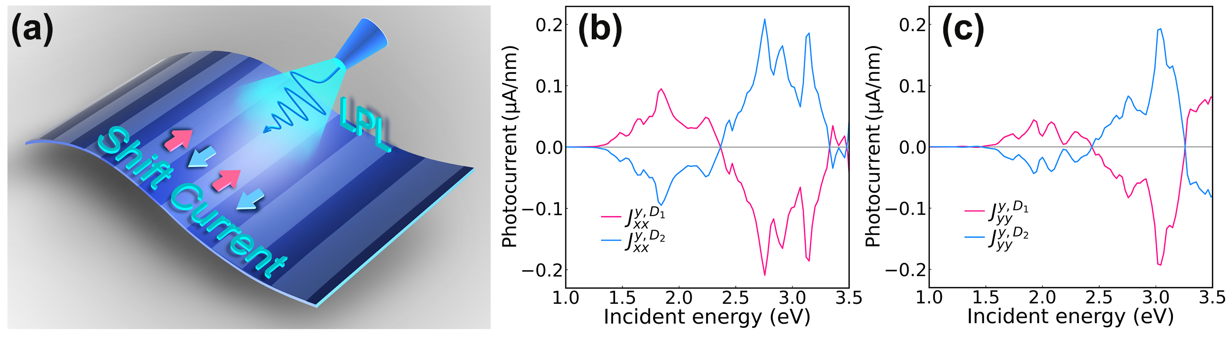
In order to precisely detect such nanostripe width variation and explore its potential applications, we suggest to resort to nanostripe-dependent BPV effect, which could convert weak above bandgap light into static electric current (or low frequency, usually THz, emission). According to nonlinear optics theory, LPL could induce shift current generation in nonmagnetic materials, which arises from the real space wavefunction center mismatch in the valence and conduction bands. In this way, optical excitation between them results in the shift of such centers and generates electric current. Such a process also reflects the topological feature of electron wavefunctions. We propose that AFE nanostripe would produce opposite flowing shift current (Figure 4a), hence one may detect nanostripe-specific short-circuit currents or open-circuit voltages. We take the LPL with a field intensity of and calculate BPV photocurrent per stripe width. The results for is plotted in Figures 4b (under -polarized LPL) and 4c (under -polarized LPL). First of all, we find that the total BPV current (summed over two antiparallel nanostripes) is always zero, consistent with the fact that the whole AFE is centrosymmetric. However, inside each nanostripe, one observes that the (). Note that under or polarized light irradiation, the current only flows along (or , parallel to nanostripe), while no current occurs along (, normal to nanostripe direction). This can be ascribed by the mirror reflection (normal to ) symmetry of the whole system. The magnitude of the 1D current density in each nanostripe is on the order of , which is sufficiently large for experimental detection. Similar photocurrents on the same magnitude order are also calculated in and (Figure S6 in SI). This nanostripe-specific photocurrent is similar as in the recently disclosed concept of hidden spin polarization 55, hidden Berry curvautre 56, and hidden Hall current 57. In all these cases, the total response functions of the system are zero, subject to specific (usually inversion or time-reversal) symmetries. But once we project them into a partial sector, they would show finite and observable signals. The fundamental mechanism is that the local symmetry of each nanostripe is lower than that of the whole system, and the removal of mirror reflection along yields finite and observable BPV currents. Here, we show that the shift current generation in 2D AFE system also belongs to such paradigm.
In conclusion, we scrutinize the light-induced structural transformation of nanostripes. According to the optomechanical theory and first-principles calculations, we suggest that one can use below bandgap light to effectively narrow the AFE nanostripe widths. By calculating the nanostripe-dependent shift current generations, we reveal hidden bulk photovoltaic shift current generations. Structural transformation of 2D ferroic materials is of great importance for fabricating advanced microelectronic devices. Our work provides a noncontacting and noninvasive strategy for manipulating AFE domains in atomic precision and would be helpful for designing nanoelectronic devices with large information storage density.
I Acknowledgments
This work is supported by the National Natural Science Foundation of China (NSFC) under Grant Nos. 21903063 and 11974270. The computational resources provided by HPC platform of Xi’an Jiaotong University are also acknowledged.
II Supporting Information
Supporting Information Available: Born effective charge, structure of fcc monolayer, supercells of AFn, band structure calculated by HSE06 hybrid functional, band-decomposed charge densities, dielectric function, and shift current photoconductivity of AF1 and AF2.
References
- Han et al. [2013] Han, S.-T.; Zhou, Y.; Roy, V. A. L. Towards the development of flexible non-volatile memories. Adv. Mater. 2013, 25, 5425–5449.
- Khan et al. [2020] Khan, A. I.; Keshavarzi, A.; Datta, S. The future of ferroelectric field-effect transistor technology. Nat. Electron. 2020, 3, 588–597.
- Junquera and Ghosez [2003] Junquera, J.; Ghosez, P. Critical thickness for ferroelectricity in perovskite ultrathin films. Nature 2003, 422, 506–509.
- Chang et al. [2016] Chang, K.; Liu, J.; Lin, H.; Wang, N.; Zhao, K.; Zhang, A.; Jin, F.; Zhong, Y.; Hu, X.; Duan, W.; Zhang, Q.; Fu, L.; Xue, Q.-K.; Chen, X.; Ji, S.-H. Discovery of robust in-plane ferroelectricity in atomic-thick SnTe. Science 2016, 353, 274–278.
- Fei et al. [2016] Fei, R.; Kang, W.; Yang, L. Ferroelectricity and phase transitions in monolayer group-IV monochalcogenides. Phys. Rev. Lett. 2016, 117, 097601.
- Liu et al. [2018] Liu, K.; Lu, J.; Picozzi, S.; Bellaiche, L.; Xiang, H. Intrinsic origin of enhancement of ferroelectricity in SnTe ultrathin films. Phys. Rev. Lett. 2018, 121, 027601.
- Song et al. [2021] Song, S.; Zhang, Y.; Guan, J.; Dong, S. Noncollinear ferrielectricity and morphotropic phase boundary in monolayer GeS. Phys. Rev. B 2021, 103, L140104.
- Liu et al. [2016] Liu, F. et al. Room-temperature ferroelectricity in CuInP2S6 ultrathin flakes. Nat. Commun. 2016, 7, 12357.
- Song et al. [2017] Song, W.; Fei, R.; Yang, L. Off-plane polarization ordering in metal chalcogen diphosphates from bulk to monolayer. Phys. Rev. B 2017, 96, 235420.
- Susner et al. [2017] Susner, M. A.; Chyasnavichyus, M.; McGuire, M. A.; Ganesh, P.; Maksymovych, P. Metal thio- and selenophosphates as multifunctional van der Waals layered materials. Adv. Mater. 2017, 29, 1602852.
- Dziaugys et al. [2020] Dziaugys, A. et al. Piezoelectric domain walls in van der Waals antiferroelectric CuInP2Se6. Nat. Commun. 2020, 11, 3623.
- Ding et al. [2017] Ding, W.; Zhu, J.; Wang, Z.; Gao, Y.; Xiao, D.; Gu, Y.; Zhang, Z.; Zhu, W. Prediction of intrinsic two-dimensional ferroelectrics in In2Se3 and other III2-VI3 van der Waals materials. Nat. Commun. 2017, 8, 14956.
- Zhou et al. [2017] Zhou, Y.; Wu, D.; Zhu, Y.; Cho, Y.; He, Q.; Yang, X.; Herrera, K.; Chu, Z.; Han, Y.; Downer, M. C.; Peng, H.; Lai, K. Out-of-plane piezoelectricity and ferroelectricity in layered -In2Se3 nanoflakes. Nano Lett. 2017, 17, 5508–5513.
- Xue et al. [2018] Xue, F.; Hu, W.; Lee, K.-C.; Lu, L.-S.; Zhang, J.; Tang, H.-L.; Han, A.; Hsu, W.-T.; Tu, S.; Chang, W.-H.; Lien, C.-H.; He, J.-H.; Zhang, Z.; Li, L.-J.; Zhang, X. Room-temperature ferroelectricity in hexagonally layered -In2Se3 nanoflakes down to the monolayer limit. Adv. Funct. Mater. 2018, 28, 1803738.
- Ju et al. [2021] Ju, L.; Tan, X.; Mao, X.; Gu, Y.; Smith, S.; Du, A.; Chen, Z.; Chen, C.; Kou, L. Controllable CO2 electrocatalytic reduction via ferroelectric switching on single atom anchored In2Se3 monolayer. Nat. Commun. 2021, 12, 5128.
- Li and Li [2016] Li, W.; Li, J. Ferroelasticity and domain physics in two-dimensional transition metal dichalcogenide monolayers. Nat. Commun. 2016, 7, 10843.
- Zhang et al. [2019] Zhang, C.; Nie, Y.; Sanvito, S.; Du, A. First-principles prediction of a room-temperature ferromagnetic Janus VSSe monolayer with piezoelectricity, ferroelasticity, and large valley polarization. Nano Lett. 2019, 19, 1366–1370.
- Lu et al. [2018] Lu, J.; Luo, W.; Feng, J.; Xiang, H. Unusual ferroelectricity in two-dimensional perovskite oxide thin films. Nano Lett. 2018, 18, 595–601.
- Ji et al. [2019] Ji, D. et al. Freestanding crystalline oxide perovskites down to the monolayer limit. Nature 2019, 570, 87–90.
- Ai et al. [2019] Ai, H.; Ma, X.; Shao, X.; Li, W.; Zhao, M. Reversible out-of-plane spin texture in a two-dimensional ferroelectric material for persistent spin helix. Phys. Rev. Mater. 2019, 3, 054407.
- Lin et al. [2019] Lin, L.-F.; Zhang, Y.; Moreo, A.; Dagotto, E.; Dong, S. Frustrated dipole order induces noncollinear proper ferrielectricity in two dimensions. Phys. Rev. Lett. 2019, 123, 067601.
- Li et al. [2018] Li, J.; Li, F.; Xu, Z.; Zhang, S. Multilayer lead-free ceramic capacitors with ultrahigh energy sensity and efficiency. Adv. Mater. 2018, 30, 1802155.
- Liu et al. [2018] Liu, Z.; Lu, T.; Ye, J.; Wang, G.; Dong, X.; Withers, R.; Liu, Y. Antiferroelectrics for energy storage applications: a review. Adv. Mater. Technol. 2018, 3, 1800111.
- Xu et al. [2022] Xu, X.; Huang, F.-T.; Du, K.; Cheong, S.-W. Multifunctionality of Li2SrNb2O7: memristivity, tunable rectification, ferroelasticity, and ferroelectricity. Adv. Mater. 2022, 202206022.
- Guo et al. [2022] Guo, A.; Bai, H.; Liang, Q.; Feng, L.; Su, X.; Van Tendeloo, G.; Wu, J. Resistive switching in Ag2Te semiconductor modulated by Ag+-Ion diffusion and phase transition. Adv. Electron. Mater. 2022, 202200850.
- Xu et al. [2020] Xu, C. et al. Two-dimensional antiferroelectricity in nanostripe-ordered In2Se3. Phys. Rev. Lett. 2020, 125, 047601.
- Zheng et al. [2018] Zheng, C. et al. Room temperature in-plane ferroelectricity in van der Waals In2Se3. Sci. Adv. 2018, 4, eaar7720.
- Xu et al. [2021] Xu, C.; Mao, J.; Guo, X.; Yan, S.; Chen, Y.; Lo, T. W.; Chen, C.; Lei, D.; Luo, X.; Hao, J.; Zheng, C.; Zhu, Y. Two-dimensional ferroelasticity in van der Waals -In2Se3. Nat. Commun. 2021, 12, 3665.
- Hohenberg and Kohn [1964] Hohenberg, P.; Kohn, W. Inhomogeneous electron Gas. Phys. Rev. 1964, 136, B864–B871.
- Kohn and Sham [1965] Kohn, W.; Sham, L. J. Self-consistent equations including exchange and correlation effects. Phys. Rev. 1965, 140, A1133–A1138.
- Kresse and Furthmüller [1996] Kresse, G.; Furthmüller, J. Efficiency of ab-initio total energy calculations for metals and semiconductors using a plane-wave basis set. Comput. Mater. Sci. 1996, 6, 15 – 50.
- Kresse and Furthmüller [1996] Kresse, G.; Furthmüller, J. Efficient iterative schemes for ab initio total-energy calculations using a plane-wave basis set. Phys. Rev. B 1996, 54, 11169–11186.
- Perdew et al. [1996] Perdew, J. P.; Burke, K.; Ernzerhof, M. Generalized gradient approximation made simple. Phys. Rev. Lett. 1996, 77, 3865–3868.
- Blöchl [1994] Blöchl, P. E. Projector augmented-wave method. Phys. Rev. B 1994, 50, 17953–17979.
- Neugebauer and Scheffler [1992] Neugebauer, J.; Scheffler, M. Adsorbate-substrate and adsorbate-adsorbate interactions of Na and K adlayers on Al(111). Phys. Rev. B 1992, 46, 16067–16080.
- Makov and Payne [1995] Makov, G.; Payne, M. C. Periodic boundary conditions in ab initio calculations. Phys. Rev. B 1995, 51, 4014–4022.
- Marzari et al. [2012] Marzari, N.; Mostofi, A. A.; Yates, J. R.; Souza, I.; Vanderbilt, D. Maximally localized Wannier functions: Theory and applications. Rev. Mod. Phys. 2012, 84, 1419–1475.
- Mostofi et al. [2008] Mostofi, A. A.; Yates, J. R.; Lee, Y.-S.; Souza, I.; Vanderbilt, D.; Marzari, N. Wannier90: A tool for obtaining maximally-localised Wannier functions. Comput. Phys. Commun. 2008, 178, 685–699.
- Zhou et al. [2018] Zhou, J.; Xu, H.; Li, Y.; Jaramillo, R.; Li, J. Opto-mechanics driven fast martensitic transition in two-dimensional materials. Nano Lett. 2018, 18, 7794–7800.
- Zhou and Zhang [2021] Zhou, J.; Zhang, S. Terahertz optics-driven phase transition in two-dimensional multiferroics. npj 2D Mater. Appl. 2021, 5, 16.
- Zhou et al. [2021] Zhou, J.; Xu, H.; Shi, Y.; Li, J. Terahertz driven reversible topological phase transition of monolayer transition metal dichalcogenides. Adv. Sci. 2021, 8, 2003832.
- Gajdoš et al. [2006] Gajdoš, M.; Hummer, K.; Kresse, G.; Furthmüller, J.; Bechstedt, F. Linear optical properties in the projector-augmented wave methodology. Phys. Rev. B 2006, 73, 045112.
- Laturia et al. [2018] Laturia, A.; Van de Put, M. L.; Vandenberghe, W. G. Dielectric properties of hexagonal boron nitride and transition metal dichalcogenides: from monolayer to bulk. npj 2D Mater. Appl. 2018, 2, 6.
- Kraut and von Baltz [1979] Kraut, W.; von Baltz, R. Anomalous bulk photovoltaic effect in ferroelectrics: A quadratic response theory. Phys. Rev. B 1979, 19, 1548–1554.
- Liu and Zhou [2022] Liu, K.; Zhou, J. Anisotropic terahertz optostriction in group-IV monochalcogenide compounds. Phys. Rev. B 2022, 105, 195406.
- Zhang et al. [2022] Zhang, Z.; Nie, J.; Zhang, Z.; Yuan, Y.; Fu, Y.-S.; Zhang, W. Atomic visualization and switching of ferroelectric order in -In2Se3 films at the single layer limit. Adv. Mater. 2022, 34, 2106951.
- Tang et al. [2022] Tang, Z.; Dai, M.; Chen, Y.; He, Q.; Luo, X.; Zheng, Y. Strain engineering the ferroelectric polarization and optical absorption in the FE-In2Se3 monolayer. J. Phys. Chem. C 2022, 126, 10181–10189.
- Shen et al. [2019] Shen, S.; Liu, C.; Ma, Y.; Huang, B.; Dai, Y. Robust two-dimensional ferroelectricity in single-layer -SbP and -SbAs. Nanoscale 2019, 11, 11864–11871.
- Wu and Zeng [2016] Wu, M.; Zeng, X. C. Intrinsic ferroelasticity and/or multiferroicity in two-dimensional phosphorene and phosphorene analogues. Nano Lett. 2016, 16, 3236–3241.
- Perdew et al. [1992] Perdew, J. P.; Chevary, J. A.; Vosko, S. H.; Jackson, K. A.; Pederson, M. R.; Singh, D. J.; Fiolhais, C. Atoms, molecules, solids, and surfaces: applications of the generalized gradient approximation for exchange and correlation. Phys. Rev. B 1992, 46, 6671–6687.
- Sun et al. [2015] Sun, J.; Ruzsinszky, A.; Perdew, J. P. Strongly constrained and appropriately normed semilocal density functional. Phys. Rev. Lett. 2015, 115, 036402.
- Grimme et al. [2010] Grimme, S.; Antony, J.; Ehrlich, S.; Krieg, H. A consistent and accurate ab initio parametrization of density functional dispersion correction (DFT-D) for the 94 elements H-Pu. J. Chem. Phys. 2010, 132, 154104.
- Popescu and Zunger [2012] Popescu, V.; Zunger, A. Extracting versus effective band structure from supercell calculations on alloys and impurities. Phys. Rev. B 2012, 85, 085201.
- Krukau et al. [2006] Krukau, A. V.; Vydrov, O. A.; Izmaylov, A. F.; Scuseria, G. E. Influence of the exchange screening parameter on the performance of screened hybrid functionals. J. Chem. Phys. 2006, 125, 224106.
- Zhang et al. [2014] Zhang, X.; Liu, Q.; Luo, J.-W.; Freeman, A. J.; Zunger, A. Hidden spin polarization in inversion-symmetric bulk crystals. Nat. Phys. 2014, 10, 387–393.
- Cho et al. [2018] Cho, S.; Park, J.-H.; Hong, J.; Jung, J.; Kim, B. S.; Han, G.; Kyung, W.; Kim, Y.; Mo, S.-K.; Denlinger, J. D.; Shim, J. H.; Han, J. H.; Kim, C.; Park, S. R. Experimental observation of hidden Berry curvature in inversion-symmetric bulk 2H-WSe2. Phys. Rev. Lett. 2018, 121, 186401.
- Chen et al. [2022] Chen, R.; Sun, H.-P.; Gu, M.; Hua, C.-B.; Liu, Q.; Lu, H.-Z.; Xie, X. C. Layer Hall effect induced by hidden Berry curvature in antiferromagnetic insulators. Natl. Sci. Rev. 2022,