Email: charlotte.boettcher@yale.edu††thanks: Present Address: IBM Research Laboratory, Zürich, Zürich, Switzerland††thanks: Present Address: New York University, New York, NY 10003, USA
Dynamical vortex transitions in a gate-tunable Josephson junction array
Abstract
We explore vortex dynamics in a two-dimensional Josephson junction array of micron-size superconducting islands fabricated from an epitaxial Al/InAs superconductor-semiconductor heterostructure, with a global top gate controlling Josephson coupling and vortex pinning strength. With applied dc current, minima of differential resistance undergo a transition, becoming local maxima at integer and half-integer flux quanta per plaquette, . The zero-field transition from the superconducting phase is split, but unsplit for the anomalous metal phase, suggesting that pinned vortices are absent or sparse in the superconducting phase, and abundant but frozen in the anomalous metal. The onset of the transition is symmetric around but skewed around , consistent with a picture of dilute vortices/antivortices on top of a checkerboard () or uniform array of vortices (). Transitions show good scaling but with exponents that differ from Mott values obtained earlier. Besides the skewing at , transitions show an overall even-odd pattern of skewing around integer values, which we attribute to vortex commensuration in the square array leading to symmetries around half-integer .
I Introduction
Two-dimensional (2D) superconductivity in thin films and Josephson junction arrays (JJAs) reveal complex classical and quantum phase transitions and rich dynamics that depend on competing energy scales and coherence, including the extensively studied superconductor-insulator transition (SIT) Jaeger et al. (1989); Fisher et al. (1991); Lee and Ketterson (1990); Goldman (2010); Gantmakher and Dolgopolov (2010); Dobrosavljevic et al. (2012), which fits into a framework of quantum critical phenomena exhibiting universal scaling Mason and Kapitulnik (1999); Yazdani and Kapitulnik (1995); Steiner and Kapitulnik (2005); Bollinger et al. (2011); Schneider et al. (2012). New classes of materials have extended SIT studies to include strictly 2D materials Allain et al. (2012); Tamir et al. (2019); Fatemi et al. (2018), hybrid super-semi heterostructures Bøttcher et al. (2018); Vaitiekėnas et al. (2020); Tosato et al. (2022); Bøttcher et al. (2022), and high-temperature superconductors Yang et al. (2019), including a transition to a topological insulating phase Wu et al. (2018). An apparent metallic phase, with saturating low-temperature finite resistance, is observed in many of these systems Kapitulnik et al. (2019), which is incompatible with simple universal scaling.
JJAs enrich the landscape by allowing controlled Coulomb interaction and frustration due to magnetic flux commensuration Newrock et al. (1999); Fazio and van der Zant (2001). Coulomb charging of Josephson-coupled islands makes the classical XY spin system into a quantum problem, with phase and charge on the islands acting as conjugate variables with an uncertainty relation. Charging also introduces a new type of disorder in the form of a random offset on the island. The periodicity of the array adds complexity in the form of a Hofstadter-like spectrum Teitel and Jayaprakash (1983); Lankhorst et al. (2018a), and possible spin glass phases Vinokur et al. (1987); Spivak and Kivelson (1991); Phillips and Dalidovich (2003). The discrete structure of a JJA also results in periodic pinning of vortices and antivortices, whose unbinding and free motion at finite temperature is described at zero magnetic field by a Berzinskii-Kosterlitz-Thouless (BKT) phase transition Halperin and Nelson (1979); Lobb et al. (1983); Newrock et al. (1999); Fazio and van der Zant (2001); Gantmakher and Dolgopolov (2010), as investigated recently in this system Bøttcher et al. (2022).
Collective pinning of vortices resulting in a zero resistance state, which has been mapped onto Mott insulator of frozen vortices Nelson and Vinokur (1993), was investigated experimentally Poccia et al. (2015); Lankhorst et al. (2018b); Mironov et al. (2020); Rezvani et al. (2020a, b); Pei et al. (2022), showing good agreement with theory, including scaling Granato (2018, 2019). In this picture, the zero-resistance state of the JJAs near nonzero integer and half integer flux quanta per plaquette, denoted frustration, , is described as vortices pinned by a combination of the periodic array potential and, importantly, collective pinning due to other vortices. Individual (noncollective) vortex pinning in the binding potential of the array has been thoroughly modelled in metallic JJAs Lobb et al. (1983); Rzchowski et al. (1990) and for intentional pinning Berdiyorov et al. (2005) and antipinning sites Berdiyorov et al. (2008), patterned to prevent dissipation in superconducting films Eley et al. (2021). We note that the Mott insulator in JJAs is closely related to the theoretical Mott insulator state at weak disorder in the 2D Bose Hubbard model. For stronger disorder the Bose Hubbard model shows a glass phase associated with individual vortex pinning POL (2013); Yao et al. (2014).
Here, we investigate a dynamic transition from the superconducting to the resistive state driven by an applied dc current, including scaling analysis of differential resistance at the transition. Previous experiments Poccia et al. (2015); Lankhorst et al. (2018b); Mironov et al. (2020); Rezvani et al. (2020a, b); Pei et al. (2022) and theory Granato (2018, 2019) interpreted the flux-dependent dynamic transition in terms of a dynamic Mott transition based on a scaling analysis that yielded exponents consistent with a Mott transition. For the gate-tuned semiconductor-based JJA investigated here, both the Josephson coupling, and the vortex pinning potential, , are tuned by a gate voltage Bøttcher et al. (2018, 2022).
Examining these transition as a dynamical phase transition, we find reasonable scaling, though with nonuniversal scaling exponents that differ from previous experiments Poccia et al. (2015); Lankhorst et al. (2018b); Pei et al. (2022). We also find different exponents on the low-field and high-field sides of the transitions. This is discussed in (Sec. IV). We conclude that our transition is not a simple Mott transition in the same universality class as previously reported. This may be due to the geometry of our structure or weaker vortex pinning in the InAs/Al system. We note that earlier studies of similar dynamic transitions were interpreted in terms of depinning of vortices from the array potential rather than as a Mott transition Benz et al. (1990); Jiang et al. (2004).
Beyond scaling, several new features of dynamical vortex transitions are presented, elucidating the underlying vortex structure. First, the dip-to-peak transition from the fully superconducting state is split at zero magnetic field, , unlike the cases of 1/2, 1, and other integer . We interpret the split peak as reflecting absent or sparse vortices at , unlike at nonzero , consistent with a BKT picture at where vortex-antivortex pairs annihilate at low temperature.
Importantly, we find that when the system is tuned (by gate voltage) into the anomalous metal phase Bøttcher et al. (2018), an unsplit peak at is instead observed. This suggests that remnant unpaired vortices and antivortices, absent in the low-temperature low-current superconducting state, are abundant at in the anomalous metal under otherwise similar conditions. The size of the splitting at in the superconducting state is found to depend on , reflecting the vortex density needed to support a dynamical transition. This is discussed in Sec. III.
Second, the evolution of the dip-to-peak transition with increasing is found to be symmetric about but highly asymmetric about and larger integers. The right-left symmetry around follows from the underlying checkerboard vortex configuration Franz and Teitel (1995); Lankhorst et al. (2018a): excess vortices are attracted to unfilled sites while deficit vortices, equivalent to antivortices, are attracted to filled sites. The situation at is quite different and naturally asymmetric: the array is full, contains one vortex per site. Any excess vortex is repelled at each site while any deficit, or antivortex, is attracted to each site, where it can annihilate. Higher integer values mirror the asymmetry at about the intervening half-integer symmetry point. This is discussed in Sec. V.
II Hybrid Array and Dynamical Vortex Transition
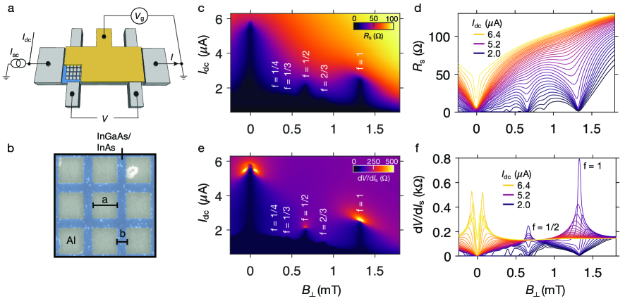
The device we investigated, shown in Fig. 1, is based on an epitaxial Al/InAs heterostructure patterned by wet etching to form a square array of islands separated by 350 nm strips of exposed semiconductor Bøttcher et al. (2018). A Ti/Au top gate, separated from the array by 40 nm of atomic-layer deposited HfO2 insulator, was used to control the carrier density in the strips between islands. The gated Hall bar has four side-probes for voltage measurements and two wide contacts at the ends for applying current, and is islands wide with between voltage probes. The sample is measured in a dilution refrigerator with a base temperature of 30 mK. All lines are filtered using QDevil rf and low-pass filters.
The top gate voltage, , controls the Josephson coupling, , between islands, driving the system from a superconducting state at V to an insulating state at V Bøttcher et al. (2018). The top gate also controls the barrier height, , (energy saddle) between vortex pinning sites (energy minima) at the corners of the square islands. Numerical studies for metallic islands suggest Rzchowski et al. (1990). Similar numerical studies have not been done for the semiconducting junctions. At intermediate gate voltages, an anomalous metallic phase was previously investigated, showing saturating gate-dependent sheet resistance at low temperature Bøttcher et al. (2018, 2022). In this work, is set to yield a superconducting state at base temperature in the absence of applied dc current and was only modified slightly toward the anomalous metal phase where indicated.
We probe the device in the nonlinear regime by measuring both the ac and dc parts of the total voltage, in a pair of side probe contacts, when total current , consisting of a varied dc part, and ac part, nA, was applied to the end contacts. A magnetic field, , was applied perpendicular to the plane of the array using an external solenoid controlled by a Keithley 2400 source-measurement unit. The area, , of one plaquette of the array, with m and nm, gives a characteristic magnetic field mT, where , corresponding to frustration . Features associated with integer values are seen in Figs. 1(c,d).
For small dc currents (A), large dips in both sheet resistance, , and differential sheet resistance, , reach zero at 0, 1/2, and 1, with moderate dips at 1/4, 1/3 and 2/3, as seen in Fig. 1(e). Increasing beyond an -dependent critical value, , results in dip-to-peak transitions in while minima in remain minima, consistent with previous experiments Poccia et al. (2015); Lankhorst et al. (2018b); Mironov et al. (2020); Rezvani et al. (2020a, b); Pei et al. (2022). The dip-to-peak transition in , visible at and , marks the onset of differential vortex motion without complete dissipative vortex flow.
III Zero-field transitions from
superconductor and anomalous metal
At zero magnetic field, , the dynamical transition appears split, so that remains a minimum as a function of , unlike and , as seen in Figs. 1(e,f). The absence of a dip-to-peak transition at , unlike for 1/2 and 1, is consistent with some previous results Poccia et al. (2015); Pei et al. (2022) but not others Jiang et al. (2004); Mironov et al. (2020); Rezvani et al. (2020b), as discussed below.
We interpret the split peak as indicating that vortices are absent or sparse at , consistent with a BKT picture in which unbound vortices pair and annihilate below a critical temperature, . This suggests that the zero-resistance state at , where vortices are absent or sparse, is qualitatively different from the zero-resistance states at and , where vortices of a single sign are abundant but frozen.
The splitting of the transition around is found to increase at lower , as seen in Figs. 1(e,f). This is seen most clearly as the downward orientation of the bright features on either side of zero field in Fig. 1(e), indicating that decreases with increasing vortex density, a signature of the role of vortex interaction in the dynamical transition. This dependence is similar the vortex-density () dependence of the vortex melting temperature Obaidat et al. (2008).
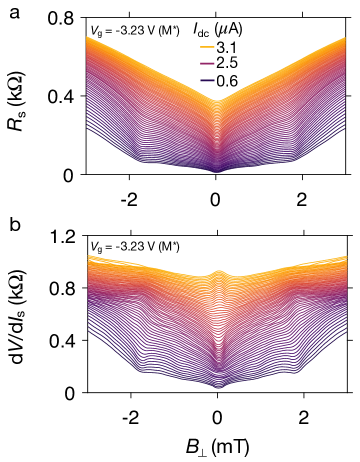
Tuning the gate voltage from V to V drives the system from the superconducting state, where falls below measurement resolution, , at low temperature, to the anomalous metal phase, where saturates at a gate-voltage dependent value, up to , at low temperature Bøttcher et al. (2018, 2022).
As shown in Fig. 2, in the anomalous metal phase a dip-to peak-transition of as a function of is observed at , while remains a minimum, similar to the dynamical transition observed at and other integer values.
The unsplit transition in the anomalous metal phase suggests that vortices and antivortices (in equal number) are present at , unlike in the superconducting phase. The nonvanishing , which characterizes the anomalous metal phase, further suggests that at least some of the remnant vortices and antivortices are mobile even at and lowest temperatures.
A picture of residual unpaired vortices at in the anomalous metal but not the superconductor is consistent with the observed vanishing of in the anomalous metal Bøttcher et al. (2022). One would anticipate that in the superconducting phase at higher temperatures, , an unsplit transition would occur at . Reported dynamical transitions at are either at elevated temperatures Jiang et al. (2004); Rezvani et al. (2020b) or in the anomalous metal phase Mironov et al. (2020), consistent with our observations.
IV Scaling and critical exponents
The dip-to-peak transition at commensurate frustration can be described as melting of a frozen vortex lattice and has been analyzed as a dynamical Mott transition Nelson and Vinokur (1993); Poccia et al. (2015); Lankhorst et al. (2018b); Granato (2018, 2019); Mironov et al. (2020); Rezvani et al. (2020a, b); Pei et al. (2022). Within this interpretation, one expects scaling at the transition among relevant parameters controlling the transition, namely the dc current bias, , and the distance, , from the commensurate frustration values, in this case 1/2 or 1.
Following Refs. Poccia et al. (2015); Lankhorst et al. (2018b), we introduce a scaling form for differential sheet resistance across the dip-to-peak transition,
| (1) |
where is a function of the scaled variable and is the scaling exponent.
A scaling exponent was measured at Poccia et al. (2015); Lankhorst et al. (2018b) and Poccia et al. (2015), in a square array of Nb islands on Au, consistent with theory for a dynamical Mott transition. At in the same system, the value was found experimentally Poccia et al. (2015); Lankhorst et al. (2018b), and later confirmed numerically Granato (2018, 2019). Other experiments investigating the dynamic transition at commensurate found different exponents Pei et al. (2022) in the triangular lattice, or did not pursue scaling analysis Mironov et al. (2020); Rezvani et al. (2020a, b).
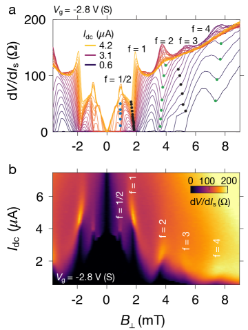
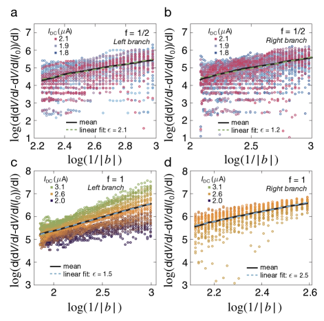
The dip-to-peak transition at was found to be right-left symmetric, while the transition at was asymmetric, as discussed in Sec. V. A consequence of the asymmetry is that the value of the commensurate frustration, , depended on [dots in Figs. 3(a,b)]. The asymmetry at also yielded different separatrices on the left and right, , , while a single separatrix value was found for (solid and dashed curves in Figs. 3(a,b). Similar asymmetries are also found at 2, 3 and 4, as seen in Fig. 4.
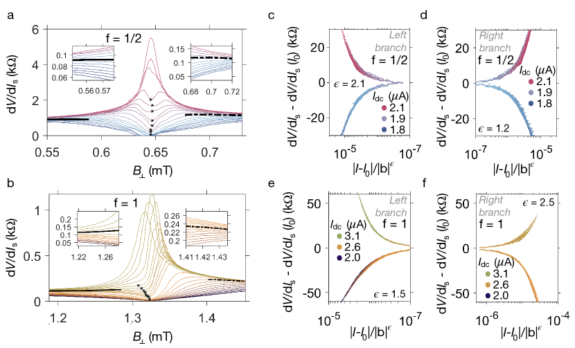
Scaling exponents were obtained by fitting the slope on a log-log plot of differential resistance after subtracting the separatrix curve, versus (see Methods). Scaled data collapse reasonably well, as seen in Figs. 3(c-f), but yield different exponents on the left and right sides of the peaks, (left) and (right) for , and (left) and (right) for , inconsistent with Poccia et al. (2015); Lankhorst et al. (2018b).
We speculate that different values for could be caused by stronger pinning potential, , in the Nb devices in Poccia et al. (2015); Lankhorst et al. (2018b) compared to the Al array studied here, leading to a different regime where dynamics may be influenced by competing effects associated with binding potential and vortex-vortex interactions. A model of vortex pinning in metallic arrays yielded, , where is the Josephson coupling, and is the single-island critical current Rzchowski et al. (1990). Taking A from Poccia et al. (2015) compared to A in our Al array suggests roughly an order of magnitude difference in .
V Skewed transitions and Even-odd structure
Figures 1(e) and 2 reveal a striking difference between the dip-to-peak transitions at and . Throughout the transition at , each curve, representing a different value, is symmetric in about the transition point. In contrast, for the transition, the curves are highly asymmetric, and in fact in the crossover from dip to peak are nearly antisymmetric lying above the high-current saturation on the right side and below it on the left side. This difference can also be seen in Fig. 1(e). The bright feature at the top of the peak, corresponding to the peak in , is flat, while the bright feature at is tilted, indicating that the peak in occurs at lower at higher .
Symmetry in around follows from the presumed checkerboard vortex configuration near Teitel and Jayaprakash (1983), which is symmetric with respect to the addition or subtraction of vortices. Excess or deficit vortices slightly above or below are expected to form a low-density superlattice on top of a base checkerboard Franz and Teitel (1995); Lankhorst et al. (2018a). The symmetry between excess and deficit vortices should persist for weak disorder, which can then pin the superlattice. In contrast, is not symmetric with respect to the addition or subtraction of dilute vortices. Excess vortices above are repelled by each site in the full lattice, while deficit vortices, or antivortices, are attracted to each site, where they can annihilate with a vortex. Within this picture, excess vortices should be weakly pinned and contribute to low-current melting Franz and Teitel (1995), while vacancies resulting from annihilation with deficit vortices should more readily pin, lowering vortex mobility. The asymmetry between excess and deficit at is a signature of vortex interaction.
Looking at integer transitions above , an even-odd structure is evident in Fig. 4, where the transition is skewed in the same direction as , while transitions at and are skewed in the opposite direction. Even-odd behavior is also visible below the transition, in the current-dependent position of the minima of , marked as dots in Fig. 4(a). Some understanding of this structure follows from the arguments above, that half-filling of the array is a symmetry point, so one might expect to be show a reflection symmetry of the behavior about , continuing by reflection about half-integers to higher integers.
While the overall even-odd pattern at integer presumably reflects the square potential of the array, the difference between (symmetric) and (asymmetric) is also seen in triangular arrays Pei et al. (2022), and reflects a more basic difference between half and full filling. Even-odd structure of dynamical transition in triangular lattices has not been reported. It will be interesting to investigate vortex filling in various lattices experimentally and numerically.
VI Discussion
We have investigated a dynamical transition from frozen to mobile vortices in a gate-tunable superconductor-semiconductor Josephson junction array. Tuning the gate into the superconducting phase, where a zero-resistance state is observed at low temperature and current, we see dip-to-peak transitions in differential resistance near frustration 1/2, 1, 2, 3, and 4, similar to previous studies in metallic arrays. Motivated by the mapping of this transition to a Mott melting transition of frozen vortices, found good scaling at the transitions but not the Mott exponent found previously, perhaps due to a weaker binding potential in our Al arrays.
The split transition at in the superconducting phase suggests that vortices are absent, not frozen, at , consistent with a BKT model in which vortices and antivortices annihilate at below a critical temperature. When the array is tuned to the anomalous metal phase, a simple unsplit transition is observed at suggesting that frozen and perhaps some unfrozen vortices are present. These observations are consistent with previously reported experiments.
The transition at is symmetric in around the transition, reflecting the symmetry of the underlying half-filled checkerboard lattice. At , on the other hand, the transition is strongly asymmetric, suggesting that excess vortices on top of an underlying full lattice melt easily, but deficit vortices (antivortices) do not. We find that the asymmetry of the transition persists to higher integers, mirrored about half integers, giving an overall even-odd pattern to transitions at higher integers. Further work is needed to understand this asymmetry, and how it depends on island and lattice geometry. This could also depend on the energetic of vortex configurations Berdiyorov et al. (2005, 2008) and binding multiple or giant vortices in the potential minima Baelus and Peeters (2002); Baelus et al. (2006).
We emphasize an general connection between these highly tunable Josephson arrays and Bose-Hubbard systems Bruder et al. (2005); Arovas et al. (2021). In these arrays, complexity is controlled by frustration and quantum by charging energy of the islands, relevant as the superconductor-insulator transition is approached.
Acknowledgments We thank A. Kapitulnik, S. Kivelson, B. Spivak, and V. Vinokur for useful discussions. Research supported by Microsoft Station Q, the Danish National Research Foundation, and a research grant (Project 43951) from VILLUM FONDEN.
Methods
Extracting scaling exponents
This subsection provides details of the scaling analysis shown in Fig. 3. The scaling exponent, , defined in Eq. 1 was extracted from the slope of a log-log plot of versus , allowing separate left and right critical currents, and .
Figure S1 shows the spread of measured values. For each value of a mean of all data was calculated. A curve through the means is show as a solid black curve. Then, a line with offset was fit to the means. The linear fit is shown as a green dashed line. The slope of the linear fit yields . The process is repeated for each value of and on the left and right sides for and . The value of extracted from the fit to takes into account the dependence of on . Values of are shown as green and back dots in Fig. 4
We note that only points near the separatrix (above and below) were included in the analysis of extracting the scaling exponent for the right branch of due to the large asymmetry, see Fig. S1(d).
References
- Jaeger et al. (1989) H. M. Jaeger, D. B. Haviland, B. G. Orr, and A. M. Goldman, Physical Review B 40, 182 (1989).
- Fisher et al. (1991) D. S. Fisher, M. P. A. Fisher, and D. A. Huse, Physical Review B 43, 130 (1991).
- Lee and Ketterson (1990) S. J. Lee and J. B. Ketterson, Physical Review Letters 64, 3078 (1990).
- Goldman (2010) A. M. Goldman, International Journal of Modern Physics B 24, 4081 (2010).
- Gantmakher and Dolgopolov (2010) V. F. Gantmakher and V. T. Dolgopolov, Physics-Uspekhi 53, 1 (2010).
- Dobrosavljevic et al. (2012) V. Dobrosavljevic, N. Trivedi, and J. M. V. Jr, Conductor Insulator Quantum Phase Transitions, Vol. 1 (Oxford University Press, United Kingdom, 2012).
- Mason and Kapitulnik (1999) N. Mason and A. Kapitulnik, Physical Review Letters 82, 5341 (1999).
- Yazdani and Kapitulnik (1995) A. Yazdani and A. Kapitulnik, Physical Review Letters 74, 3037 (1995).
- Steiner and Kapitulnik (2005) M. Steiner and A. Kapitulnik, Physica C 422, 16 (2005).
- Bollinger et al. (2011) A. T. Bollinger, G. Dubuis, J. Yoon, D. Pavuna, J. Misewich, and I. Bozovic, Nature 472, 458 (2011).
- Schneider et al. (2012) R. Schneider, A. G. Zaitsev, D. Fuchs, and H. v. Löhneysen, Physical Review Letters 108, 257003 (2012).
- Allain et al. (2012) A. Allain, Z. Han, and V. Bouchiat, Nat. Mater. 11, 590 (2012).
- Tamir et al. (2019) I. Tamir, A. Benyamini, E. J. Telford, F. Gorniaczyk, A. Doron, T. Levinson, D. Wang, F. Gay, B. Sacépé, J. Hone, K. Watanabe, T. Taniguchi, C. R. Dean, A. N. Pasupathy, and D. Shahar, Science Advances 5, eaau3826 (2019).
- Fatemi et al. (2018) V. Fatemi, S. Wu, Y. Cao, L. Bretheau, Q. D. Gibson, K. Watanabe, T. Taniguchi, R. J. Cava, and P. Jarillo-Herrero, Science 362, 926 (2018).
- Bøttcher et al. (2018) C. G. L. Bøttcher, F. Nichele, M. Kjaergaard, H. J. Suominen, J. Shabani, C. J. Palmstrøm, and C. M. Marcus, Nature Physics 14, 1138 (2018).
- Vaitiekėnas et al. (2020) S. Vaitiekėnas, P. Krogstrup, and C. M. Marcus, Physical Review B 101, 060507 (2020).
- Tosato et al. (2022) A. Tosato, V. Levajac, J.-Y. Wang, C. J. Boor, F. Borsoi, M. Botifoll, C. N. Borja, S. Martí-Sánchez, J. Arbiol, A. Sammak, M. Veldhorst, and G. Scappucci, arXiv (2022), 2206.00569 .
- Bøttcher et al. (2022) C. G. L. Bøttcher, F. Nichele, J. Shabani, C. J. Palmstrøm, and C. M. Marcus, (2022), 2210.00318 .
- Yang et al. (2019) C. Yang, Y. Liu, Y. Wang, L. Feng, Q. He, J. Sun, Y. Tang, C. Wu, J. Xiong, W. Zhang, X. Lin, H. Yao, H. Liu, G. Fernandes, J. Xu, J. M. Valles, J. Wang, and Y. Li, Science 366, 1505 (2019).
- Wu et al. (2018) S. Wu, V. Fatemi, Q. D. Gibson, K. Watanabe, T. Taniguchi, R. J. Cava, and P. Jarillo-Herrero, Science 359, 76 (2018).
- Kapitulnik et al. (2019) A. Kapitulnik, S. A. Kivelson, and B. Spivak, Rev. Mod. Phys. 91, 011002 (2019).
- Newrock et al. (1999) R. Newrock, C. Lobb, U. Geigenmüller, and M. Octavio (1999) pp. 263–512.
- Fazio and van der Zant (2001) R. Fazio and H. van der Zant, Physics Reports 355, 235 (2001).
- Teitel and Jayaprakash (1983) S. Teitel and C. Jayaprakash, Physical Review Letters 51, 1999 (1983).
- Lankhorst et al. (2018a) M. Lankhorst, A. Brinkman, H. Hilgenkamp, N. Poccia, and A. Golubov, Condensed Matter 3, 19 (2018a).
- Vinokur et al. (1987) V. M. Vinokur, L. B. loffe, A. I. Larkin, and Feigel’man, and M. V., Sov. Phys. JETP 66, 198 (1987).
- Spivak and Kivelson (1991) B. I. Spivak and S. A. Kivelson, Physical Review B 43, 3740 (1991).
- Phillips and Dalidovich (2003) P. Phillips and D. Dalidovich, Science 302, 243 (2003).
- Halperin and Nelson (1979) B. I. Halperin and D. R. Nelson, Journal of Low Temperature Physics 36, 599 (1979).
- Lobb et al. (1983) C. J. Lobb, D. W. Abraham, and M. Tinkham, Physical Review B 27, 150 (1983).
- Nelson and Vinokur (1993) D. R. Nelson and V. M. Vinokur, Physical Review B 48, 13060 (1993).
- Poccia et al. (2015) N. Poccia, T. I. Baturina, F. Coneri, C. G. Molenaar, X. R. Wang, G. Bianconi, A. Brinkman, H. Hilgenkamp, A. A. Golubov, and V. M. Vinokur, Science 349, 1202 (2015).
- Lankhorst et al. (2018b) M. Lankhorst, N. Poccia, M. P. Stehno, A. Galda, H. Barman, F. Coneri, H. Hilgenkamp, A. Brinkman, A. A. Golubov, V. Tripathi, T. I. Baturina, and V. M. Vinokur, Physical Review B 97, 1 (2018b).
- Mironov et al. (2020) A. Y. Mironov, S. V. Postolova, and D. A. Nasimov, Journal of Experimental and Theoretical Physics 131, 298 (2020).
- Rezvani et al. (2020a) S. J. Rezvani, D. D. Gioacchino, C. Gatti, C. Ligi, M. C. Guidi, S. Cibella, M. Fretto, N. Poccia, S. Lupi, and A. Marcelli, Condensed Matter 5, 33 (2020a).
- Rezvani et al. (2020b) J. Rezvani, D. D. Gioacchino, C. Gatti, N. Poccia, C. Ligi, S. Tocci, M. C. Guidi, S. Cibella, S. Lupi, and A. Marcelli, Acta Physica Polonica A 137, 17 (2020b), 1912.05847 .
- Pei et al. (2022) Z.-X. Pei, W.-G. Guo, and X.-G. Qiu, Chinese Physics B 31, 037404 (2022).
- Granato (2018) E. Granato, Physical Review B 98, 094511 (2018).
- Granato (2019) E. Granato, Physical Review B 100, 104517 (2019).
- Rzchowski et al. (1990) M. S. Rzchowski, S. P. Benz, M. Tinkham, and C. J. Lobb, Physical Review B 42, 2041 (1990).
- Berdiyorov et al. (2005) G. R. Berdiyorov, M. V. Milošević, and F. M. Peeters, Physical Review Letters 96, 207001 (2005).
- Berdiyorov et al. (2008) G. R. Berdiyorov, V. R. Misko, M. V. Milošević, W. Escoffier, I. V. Grigorieva, and F. M. Peeters, Physical Review B 77, 024526 (2008).
- Eley et al. (2021) S. Eley, A. Glatz, and R. Willa, Journal of Applied Physics 130 (2021), 10.1063/5.0055611.
- POL (2013) Comptes Rendus Physique 14, 712 (2013), disordered systems / Systèmes désordonnés.
- Yao et al. (2014) Z. Yao, K. P. C. da Costa, M. Kiselev, and N. Prokof’ev, Physical Review Letters 112, 225301 (2014).
- Benz et al. (1990) S. P. Benz, M. S. Rzchowski, M. Tinkham, and C. J. Lobb, Physical Review B 42, 6165 (1990).
- Jiang et al. (2004) Z. Jiang, D. A. Dikin, V. Chandrasekhar, V. V. Metlushko, and V. V. Moshchalkov, Applied Physics Letters 84, 5371 (2004).
- Franz and Teitel (1995) M. Franz and S. Teitel, Physical Review B 51, 6551 (1995).
- Obaidat et al. (2008) I. M. Obaidat, U. A. Khawaja, and M. Benkraouda, Superconductor Science and Technology 21, 085004 (2008).
- Baelus and Peeters (2002) B. J. Baelus and F. M. Peeters, Physical Review B 65, 104515 (2002).
- Baelus et al. (2006) B. J. Baelus, A. Kanda, N. Shimizu, K. Tadano, Y. Ootuka, K. Kadowaki, and F. M. Peeters, Physical Review B 73, 024514 (2006).
- Bruder et al. (2005) C. Bruder, R. Fazio, and G. Schön, Annalen der Physik 14 (2005), 10.1002/andp.200510157.
- Arovas et al. (2021) D. P. Arovas, E. Berg, S. A. Kivelson, and S. Raghu, Annual Review of Condensed Matter Physics 13, 1 (2021).