resize
Non-Uniform Superlattice Magnetic Tunnel Junctions
Abstract
We propose a new class of non-uniform superlattice magnetic tunnel junctions (Nu-SLTJs) with the Linear, Gaussian, Lorentzian, and Pöschl-teller width and height based profiles manifesting a sizable enhancement in the TMR() with a significant suppression in the switching bias(9 folds) owing to the physics of broad-band spin filtering. By exploring the negative differential resistance region in the current-voltage characteristics of the various Nu-SLTJs, we predict the Nu-SLTJs offer fastest spin transfer torque switching in the order of a few hundred picoseconds. We self-consistently employ the atomistic non-equilibrium Green’s function formalism coupled with the Landau–Lifshitz–Gilbert–Slonczewski equation to evaluate the device performance of the various Nu-SLTJs. We also present the design of minimal three-barrier Nu-SLTJs having significant TMR() and large spin current for ease of device fabrication. We hope that the class of Nu-SLTJs proposed in this work may lay the bedrock to embark on the exhilarating voyage of exploring various non-uniform superlattices for the next generation of spintronic devices.
I INTRODUCTION
The research in the ambit of magnetic devices has witnessed an augmented proliferation with the development of magnetic tunnel junctions (MTJs) owing to their versatile applications in nanoscale spintronics. Ever since the pioneering discovery of tunnel magnetoresistance(TMR)Parkin et al. (2004) and spin transfer torque(STT)Berger (1996); Slonczewski (1996), MTJs are being explored as the building blocks for energy-efficient integrated circuits of the beyond Moore era. Along with the STT- magnetoresistive random access memory (MRAM) and the spin torque nano oscillators(STNO), the utility of MTJs have been extended across the diverse disciplines of current imagingLe Phan et al. (2006), magnetoencephalographyKanno et al. (2022), weapon detectionRudin and Bramble (1997), wireless communicationChen et al. (2016), magnetic recordingBraganca et al. (2010) and biomedical imagingRobbes (2006).
Besides, the research of materializing the STT-MRAMs and the spin torque nano oscillators(STNOs) have predominantly anchored the novel literature of spintronic devices for their potential applications in the immediate futureKrivorotov et al. (2005); Choi et al. (2014); Cheng et al. (2016); Bhattacharjee et al. (2018); Jiang et al. (2004); Mangin et al. (2006); Diao et al. (2007); Santos et al. (2020). A confluence of high-speed operation, non-volatility, durability, and high density along with CMOS compatibility have eventuated the STT-MRAM as a viable candidate for state-of-the-art storage devicesIkeda et al. (2007); Apalkov et al. (2013); Khvalkovskiy et al. (2013); Bhatti et al. (2017); Prenat et al. (2007). Apart from that, the broad tuning rangeBonetti et al. (2010), nanoscopic footprintsVillard et al. (2009), and effortless integration with cutting-edge CMOS technology have conferred the STNO a pivotal role in various frequency modulation schemes, wireless radio-frequency communication, and futuristic read headsZeng et al. (2013); Mizushima et al. (2010); Braganca et al. (2010).
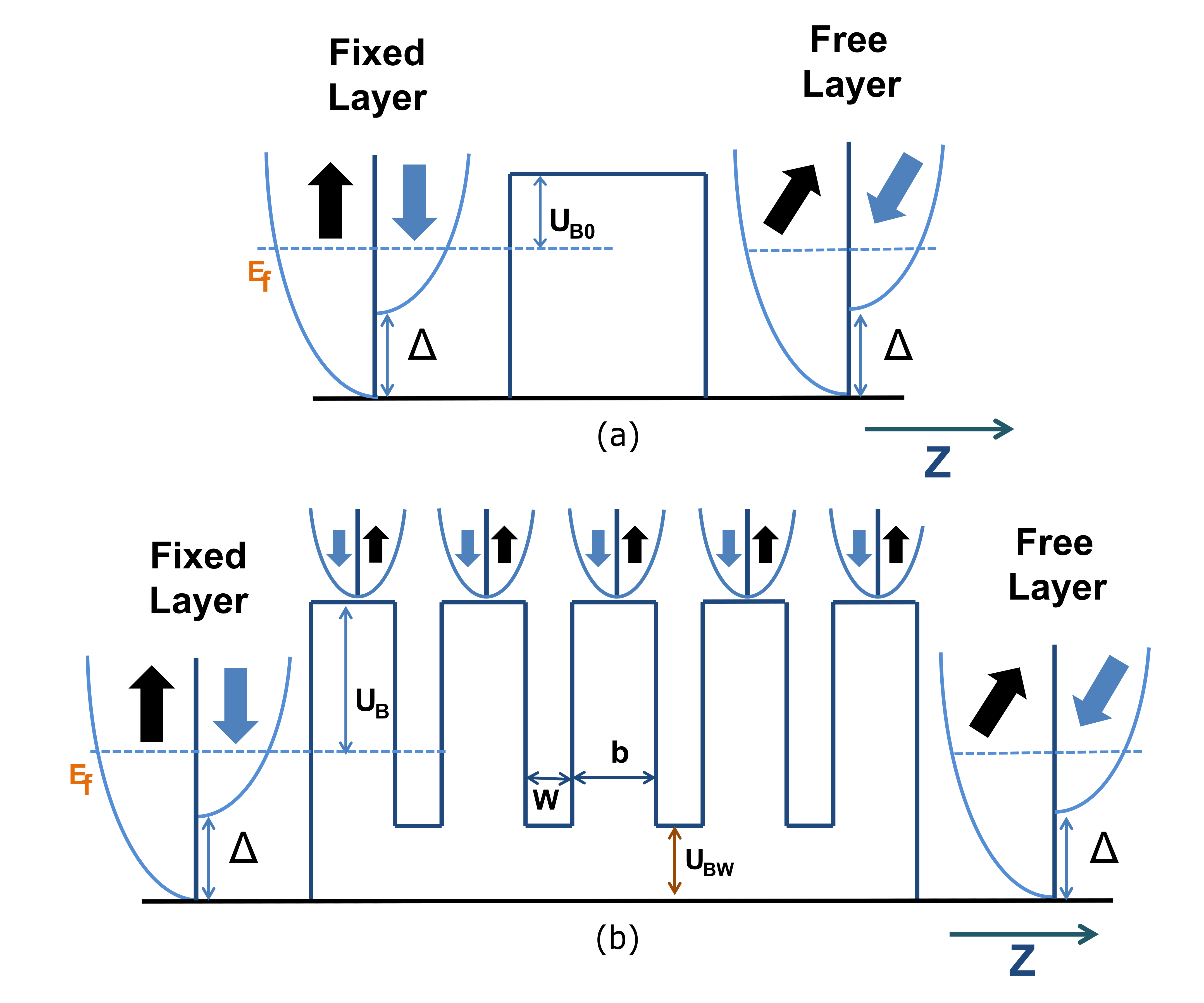
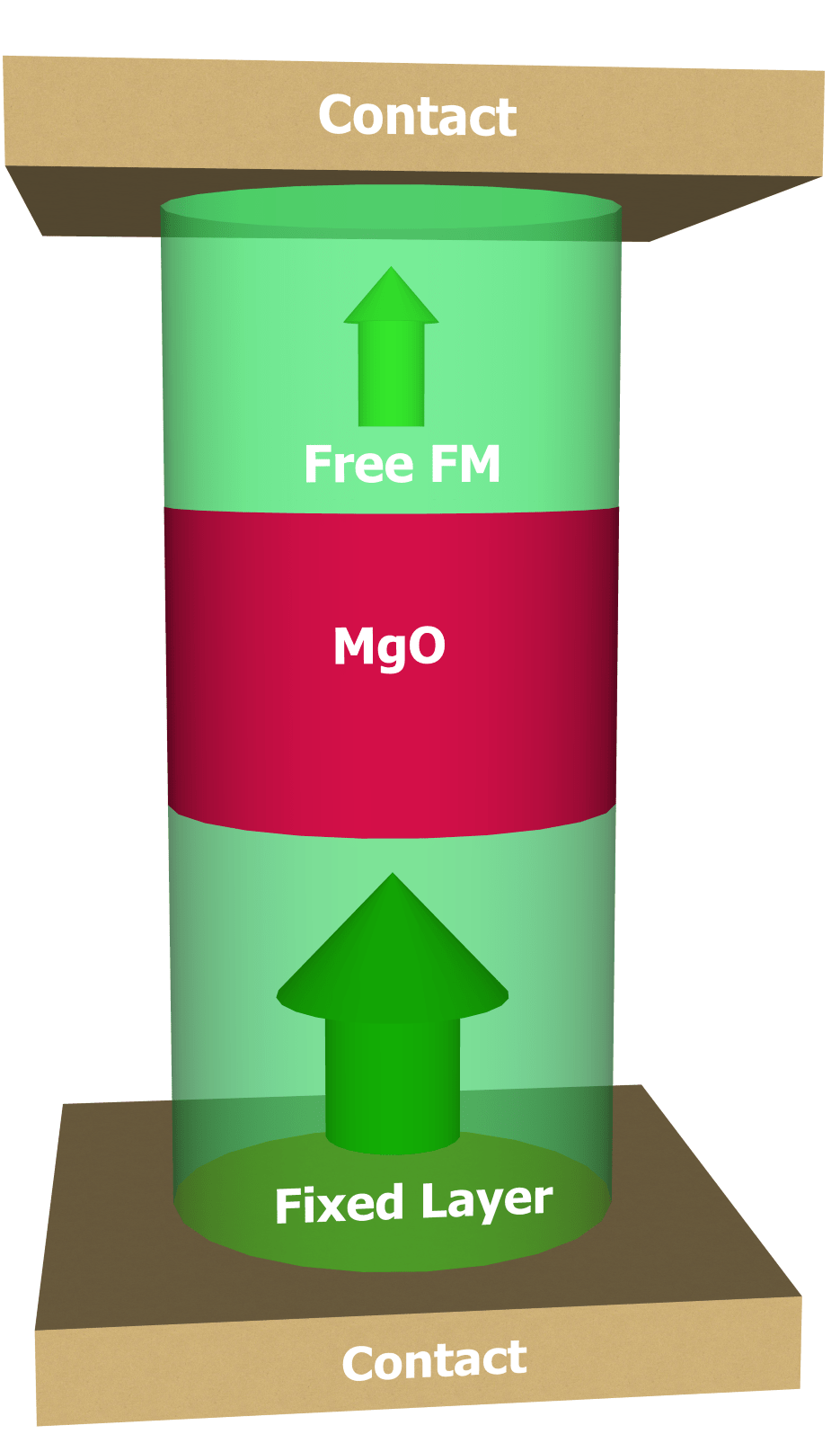
A typical MTJ comprises a free and fixed ferromagnet(FM) separated by an insulating material(MgO)Butler et al. (2001) as depicted in Fig. 1(a). An MTJ offers different resistances in the parallel() and anti-parallel() configurations of the magnetization of the fixed and free FMs due to spin-dependent tunneling of the electrons, which is quantified by the TMR(%)%.
The magnetization of the free FM can be switched using the STT exerted by the spin-polarized electrons coming from the fixed FMBerger (1996); Slonczewski (1996); Meo et al. (2022). Perpendicular magnetic anisotropy (PMA) facilitates the magnetization of the fixed and free layers of the MTJ to align perpendicularly to the film plane. A typical PMA-MTJ (p-MTJ) yields fast switching in the order of a few nanoseconds along with lower power consumption and superior thermal stability compared to in-plane MTJsSlaughter et al. (2016). However, a faster switching demands a high current density that undermines the aspirations of energy-efficient writingApalkov et al. (2013); Endoh et al. (2020). One may address this problem while applying the spin-orbit torque(SOT) to the free FM, where the switching current does not tunnel through the oxide layer of the MTJ, resulting in a significant reduction in power consumptionMeo et al. (2022). But, SOT-switching is not deterministic in the p-MTJs, and one may need to apply some external magnetic field for deterministic switchingByun et al. (2021). At the same time, the separate reading and writing path in the SOT-driven MTJs increases the complexity of the fabrication process. Further, neither type of the devices (STT and SOT driven p-MTJs) yield an ultra-high sensitivity due to their inadequate TMR(%) in comparison to the proposed devices.
Technologically relevant applications based on the MTJ devices require a high TMR(%) and a low switching biasSharma et al. (2017, 2016, 2018a).
There have been consistent efforts to propose regular superlattice-based MTJs (SLTJs) to provide an ultra-high TMR() and reduction in switching biasChen and Hsueh (2014); Chen et al. (2015) owing to the physics of spin selective resonant filtering. Various 2D in-plane and van der waal(vdw) heterostructures have been explored in the quest of achieving a high TMR and a decimated power consumption. For example, the first principle calculation of vdw heterostructures such as Co/MoS2/graphene/MoS2/CoDevaraj and Tarafder (2021) and Au/graphene /2 monolayer of CrI3 / graphene /AuZhang et al. (2022) have predicted to engender a TMR of 1270% and 2 respectively. On the other hand, ab-initio calculations of in-plane heterostructures like VS2/MoS2/VS2 have revealed a TMR of Zhao et al. (2018). Along with these proposals, there have been consistent experimental efforts to realize superlattice-based MTJs(SLTJs) after the successful fabrications of various multiple-quantum well-based magnetic tunnel junctionsTao et al. (2019); Bhattacharjee et al. (2016); Tseng et al. (2020).
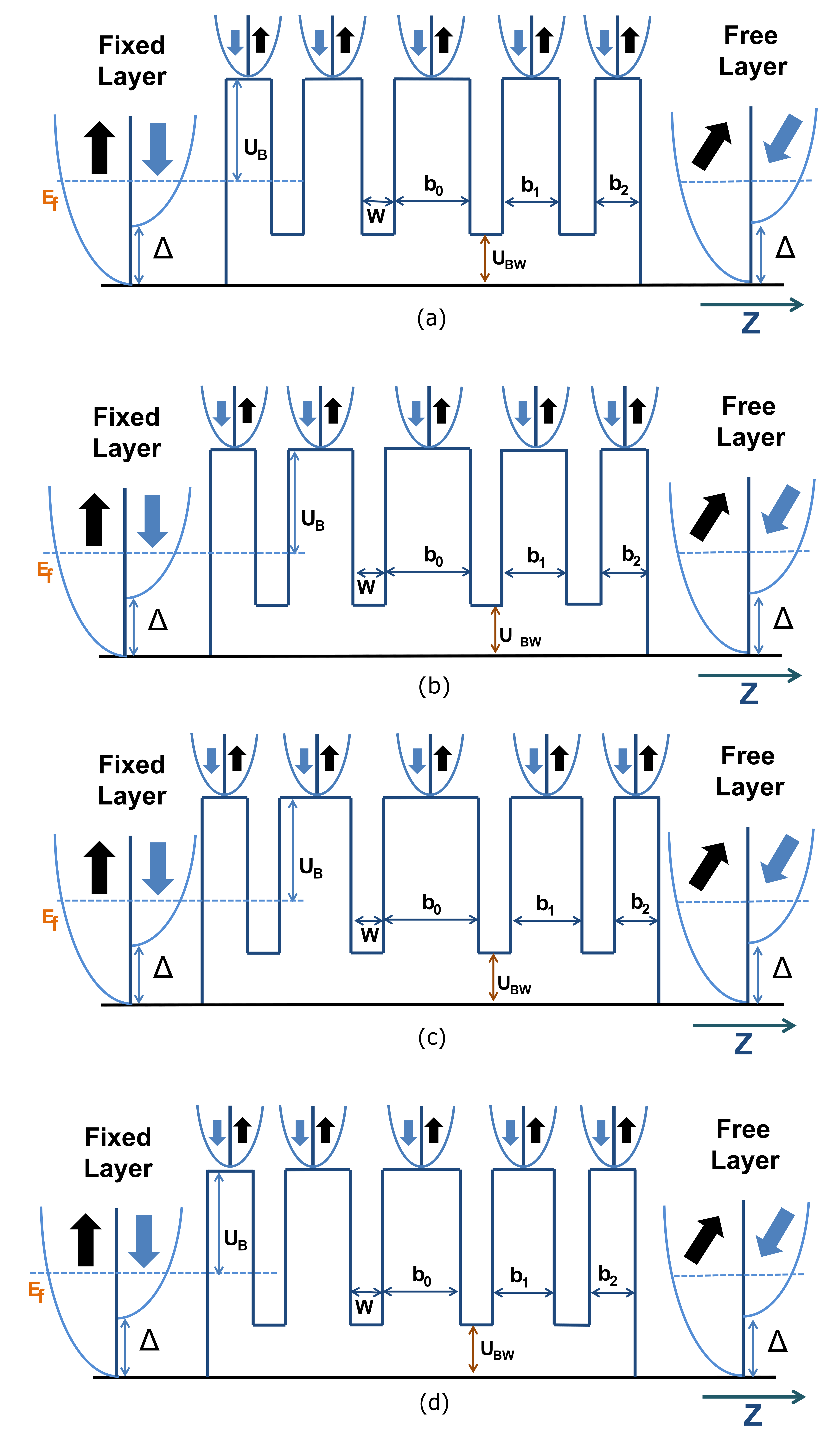
Relying on this patronage, we propose a compendium of various nonuniform-SLTJs(Nu-SLTJs) for spintronic applications with the Gaussian, Linear, Lorentzian, and Pöscl-Teller width(Fig. 3) and height(Fig. 4) profilesDiez et al. (2000); Gómez et al. (1999); Sánchez-Arellano et al. (2019). The physics of spin selective broad-band filtering (see Appendix A) in these proposed Nu-SLTJs culminates furtherance in the TMR(%) and a significant reduction in the switching bias of the proposed devices along with minimal layered Nu-SLTJs design.
In order to benchmark the switching biases of the various proposed devices (PDs) against the regular MTJ, we define a performance index as the suppression in the switching bias(SSB) given by
| (1) |
where PC(APC) denotes the parallel(anti-parallel) configuration, and represents the switching biases applied to the trilayer MTJ(PD) for the APC to PC and the PC to APC switching, and SB represents the switching bias as discussed in Appendix A.
We chronicle this article by first describing the tight-binding device Hamiltonian and the self-consistent coupling of the Landau–Lifshitz–Gilbert–Slonczewski equation with the Non-equilibrium Green’s Function formalism in section II, thereby providing a theoretical foundation behind our computational framework. Subsequently, we lay down the detailed design of various width(W) and height(H)-based Nu-SLTJs(W-SLTJs and H-SLTJs) along with the simulation results of each device in the section III. It incorporates the spin and charge current characteristics along with the switching dynamics of the various Nu-SLTJs comprised of Linear width(III.2), Gaussian width(III.3), Lorentzian width(III.4), Pöschl-Teller width(III.5), Linear height(III.6), Gaussian height(III.7), Lorentzian height(III.8) and Pöschl-Teller height(III.9) profiles including the trilayer MTJ(III.1). We also demonstrate the relevance of the Nu-SLTJs in order to address the shortcomings of a regular SLTJ. Thereafter, we analyse the performances of the aforementioned devices at higher voltages in section IV while envisioning their possible applications in the STNOs. Thenceforth in section.V we compare various performance indices of the Nu-SLTJs in Tab.(1), followed by the conclusion in section VI, thereby abridging a synopsis of the study.
II Mathematical Modelling and Simulation Details
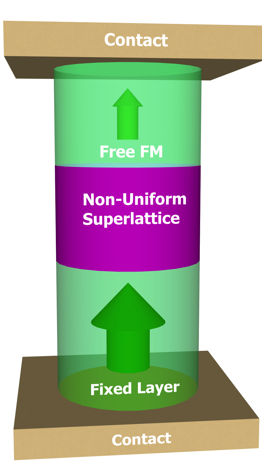
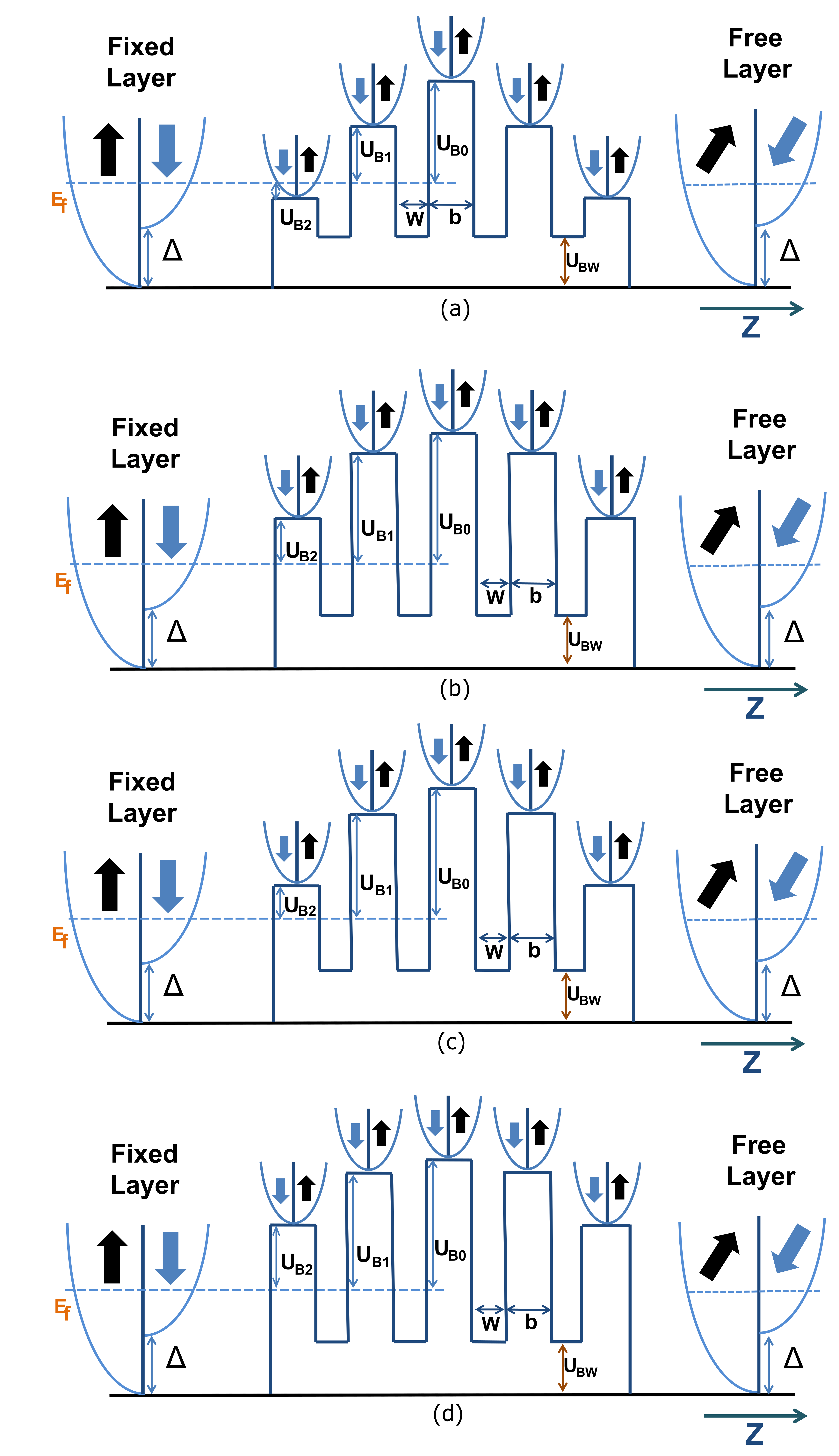
We begin with the description of the device schematics of the tri-layer MTJ and the Nu-SLTJ depicted in Figs. 1(a) and 1(b). The Nu-SLTJ is realized by sandwiching a non-uniform heterostructure comprised of insulator(I)-normal metal(NM)- - -I-NM-I- - -NM-I layers between the fixed and free FMs as shown in Figs.34. We have used MgO as an insulator to implement the W-SLTJs, whereas H-SLTJs have been realized by utilizing a stoichiometrically substituted MgxZn1-xOTian et al. (2014) as barrier region. One can estimate the band gap of such stoichiometrically substituted semiconductors via the first-order interpolation methodLi et al. (2014). The quantum(q)-well regions of the non-uniform superlattice may consist of an NM (Ru,Cu,Ti etc.) such that the dimension of the q-wells remain significantly smaller than spin coherent lengthSharma et al. (2021); Chen and Hsueh (2014); Sharma et al. (2018b); Chen et al. (2015).
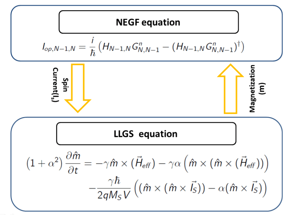
To analyse the quantum transport through mesoscopic devices such as an MTJ or an Nu-SLTJ, we first describe the relationship of the Hamiltonian matrix [H] with the energy-resolved spin-dependent retarded Green’s function matrix [G(E)], given byDatta (2018)
| (2) | |||
| (3) |
where the Hamiltonian matrix [H]=[H0]+[U0] comprises the nearest neighbour tight-binding Hamiltonian [H0] and the applied potential matrix [U0], while represents an identity matrix with dimensions of the device Hamiltonian [H]. In equation.3, we formulate the coupling of the Hamiltonian matrix corresponding to the device region [H] with the self-energy matrices of the fixed and the free FMs described via and , respectively. We describe the ferromagnetic behavior of the contacts by the Stoner model Ralph and Stiles (2008), with conduction band exchange splitting (), Fermi energy (Ef), and effective mass (mfm). Based on the above-mentioned formulation, we compute the Hamiltonian matrix[H], the self-energy matrix (), and the energy-resolved spin-dependent retarded Green’s function matrix[G(E)] for the tight binding frameworkSharma et al. (2021). In order to take care of the current conduction at various modes, we include the respective transverse mode energies() to the diagonal elements of the device Hamiltonian given by Et=, where and represents wave vectors along the and axis, while the electron transport takes place along the direction. Sharma et al. (2021).
In the next step, we describe the density of electrons in the channel region by the diagonal elements of the energy resolved electron correlation matrix [], given by
| (4) |
| (5) |
where the quantities and denotes the spin-dependent broadening matrices Datta (2005) of the fixed and free FM contacts, respectively. To construct the applied potential matrix[U0], we assume a linear drop across the oxide region and no drop across the metal layers. The Fermi-Dirac distribution functions related to the free(f) and fixed(F) FMs are denoted as and , respectively. We apply the boundary conditions by assuming and , where is the applied voltage. The current between th and th lattice points of the device is described by the current operator Iop Datta (1997), given by
| (6) |
The charge current through the device is defined as
| (7) |
and spin current is given by
| (8) |
where denotes the Pauli spin-matrices along , , directions.
The magnetization dynamics of the free layer in the presence of an applied magnetic field and spin current is calculated using the self consistent coupling of the NEGF formalism with the Landau–Lifshitz–Gilbert–Slonczewski (LLGS) equation as described in Fig. 5. The LLGS equationSlonczewski (1996) is given by
| (9) |
where represents the direction of magnetization of the free layer, represents the Gilbert damping parameter and is called the gyromagnetic ratio of the electron, represents the saturation magnetization, represents the volume of the FM contacts. The effective magnetic field is given by , with being the applied field which is taken as zero for our simulations, and represents the uniaxial magnetic anisotropy of the FMs with PMA.
The spin current is decomposed into three components such that
where and represents a unit vector along the direction of the fixed and free FM, respectively and apart from that the Is|| and Is⟂ denotes the Slonczewski and field like term.
Further, the equation.9 can be divided in two factors such that
| (10) |
where, the spinning factor(SF) describes the angular frequency of the magnetization around the easy axis and the damping factor(DF) represents the rate of change of the angle between the easy axis and the magnetization.
After plugging in the value of the in equation.9 the spinning factor(SF) can be re-casted as
| (11) |
Similarly, the expression of the damping factor(DF) can be simplified as
| (12) |
We can safely ignore the term in Eq. 12 as it is much smaller than . Hence, the critical current for switching is given as . The value of the critical switching current for an in plane MTJ under the macro-spin assumption is given by Is||,c=, where and denotes the in-plane anisotropy and the demagnetizing field, respectivelyRalph et al. (2011). It is worthwhile mentioning that the value of the is mostly one order higher compared to the which causes a significant hike in power consumption. One may reduce the impact of the while utilizing FMs with PMATudu and Tiwari (2017), where the direction of the magnetization aligns perpendicularly to the thin film planePrakash et al. (2017). The effective magnitude of the perpendicular anisotropy is given as , where and denotes the thickness and the interface PMA factor of an FM thin film, respectively. The inter-facial PMA dominates the when the width of the FM is made smaller beyond a critical thicknessIkeda et al. (2010). The value of the critical current is given by .
In this work, we have used CoFeBMiao et al. (2006) for the FM contacts with the Fermi energy eV and conduction band exchange splitting eVSharma et al. (2018b) while assuming the effective masses of an electron in the MgO barriers, in the NM quantum wells and in the FM contacts as , and , respectively Datta et al. (2011), where denotes the free-electron-mass. We have taken the barrier height between CoFeB and MgO as U eV above Fermi level Datta (2012) and considered the conduction band offset between the FM and the NM layer as UBW=0.4 eV. The NM q-wells have the same thickness of nm to keep them within the fabrication limits Tao et al. (2019); Yang et al. (2015). We have considered the minimum oxide width as nm which is the least thickness of the MgO that can be deposited reliably Deac et al. (2008). We have taken the thickness of the free FM as 1.3 nm Ikeda et al. (2010) and have considered the cross-sectional area of the FM contacts as 0.25 nm2 so that the magnetization dynamics of the free FM can be described by a macro-spin model Sato et al. (2014). The value of the saturation magnetization is considered as emu/cc and the perpendicular uni-axial magnetic anisotropy is taken as =3.3 k OeGajek et al. (2012). The thermal stability factor is given by . The value of the damping parameter and gyromagnetic ratio are taken as and MHz/Oe, respectively.
After evaluating all the parameters in the equation of the critical current given by I, we obtain an Is||,c of 0.0106 mA. When the Is|| becomes equal to the Is||,c, the damping force(DF) acting on the free layer becomes zero and the relative angle() between the easy axis and magnetization of the free layer becomes constant. In order to perform the switching of the free FM, we need to supply a switching current, higher than the critical current, so that the spin current() induced anti-damping force ( dominates over the damping due to the uniaxial magnetic anisotropy(). Whilst the Is|| is near the critical current, the effective damping force acting on the free layer becomes negligible. Hence the switching of the magnetization takes a longer time. To avoid this, we apply a spin current(Is||=0.0127 mA), which is 20% higher than the critical current (see Appendix:A) thereby ensuring a comfortable switching.
III Device Details and Simulation Results
In the wide design landscape of non-uniform superlattices, we first explore the TMR(%) and Is|| of various Nu-SLTJs with respect to the number of barriers (oxide layers) as shown in the Fig. 6 (at V=5mV).
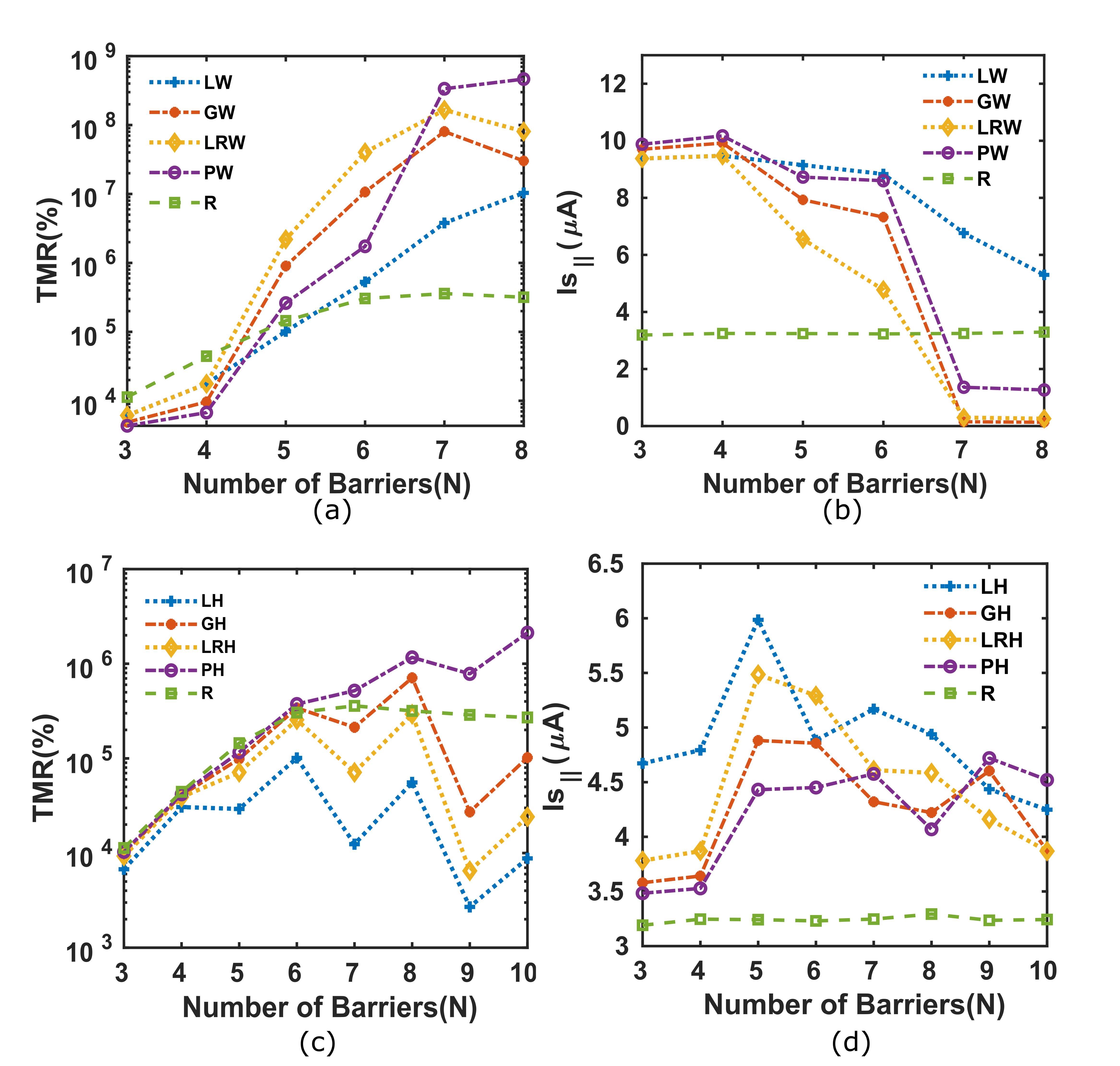
It can be inferred from Fig. 6(a) & (b) that in W-SLTJs, the TMR(%) first increases with the number of barriers and then decreases whereas Is|| decreases monotonically. As the number of barriers(N) goes from 4 to 5, we see a significant increase in the TMR(%) along with a respectable . At N=6, although a higher TMR(%) is achieved but Is|| drops even further. In our design of width-based SLTJs, the thickness of the central barriers increases with to keep the width of terminal barriers within fabrication limits Deac et al. (2008). The thickness of the central oxide in the GW-SLTJ reaches 2.1 nm at because of the exponent factor (see Eq. 13). It vanishes the spin selective transmission through the GW-SLTJ for , resulting in a decimated . A similar behaviour is noticed for both the PW and LRW-SLTJs making them dysfunctional for except for the LW-SLTJ.
We present the dependence of the TMR(%) and Is|| of the H-SLTJs with respect to the number of barriers in Fig. 6. As we increase the number of barriers from three to four, we see a slight increase in the Is||(Fig. 6(d)). This can be attributed to the fact that an increase in the number of barriers increases the number of resonant peaks and the neighborhood Bloch states, which gives rise to a better broad-band spin filtering. In the H-SLTJs, when we have odd number of barriers, there is only one central barrier with a scattering potential of 3.01 eV. But for H-SLTJs with even number of barriers, there are two central barriers with a scattering potential of 3.01 eV. Therefore, for the even number of barriers, the H-SLTJs provide a larger hindrance to the electron tunneling and hence offer a poorer Is|| and a better TMR. as we increase the number of barriers in the H-SLTJs, the terminal barriers possess lower barrier heights. Consequently, they do not hinder electron tunneling significantly and may help to engender a better broad-band transmission while ameliorating the Is||. Along similar lines, an improvement in the transmission might deteriorate the ratio of the transmissions in the PC and the APC within the Fermi window while reducing the TMR. Therefore, the H-SLTJs do not show monotonic behavior akin to the W-SLTJs. Figure. 6(c)&(d) illustrates that the of the H-SLTJs peaks at N=5 along with a sizeable TMR(%).
Hence, in the subsequent subsections, we present detailed designs of the W and H-SLTJs with n=5 and draw a performance comparison with a regular SLTJ and a trilayer MTJ in Tab. 1. Figure. 6 exemplifies that the regular SLTJ(R-SLTJ) offers an adequate TMR(%) in comparison to the Nu-SLTJs but fails to provide a respectable . Hence, Nu-SLTJs emerge as viable alternatives for meager power consumption and faster switching.
III.1 Characteristics of a Tri-layer MTJ
We first explore the electrical characteristics of a trilayer MTJ shown in Fig. 1(a), along with the STT-switching of the free FM.
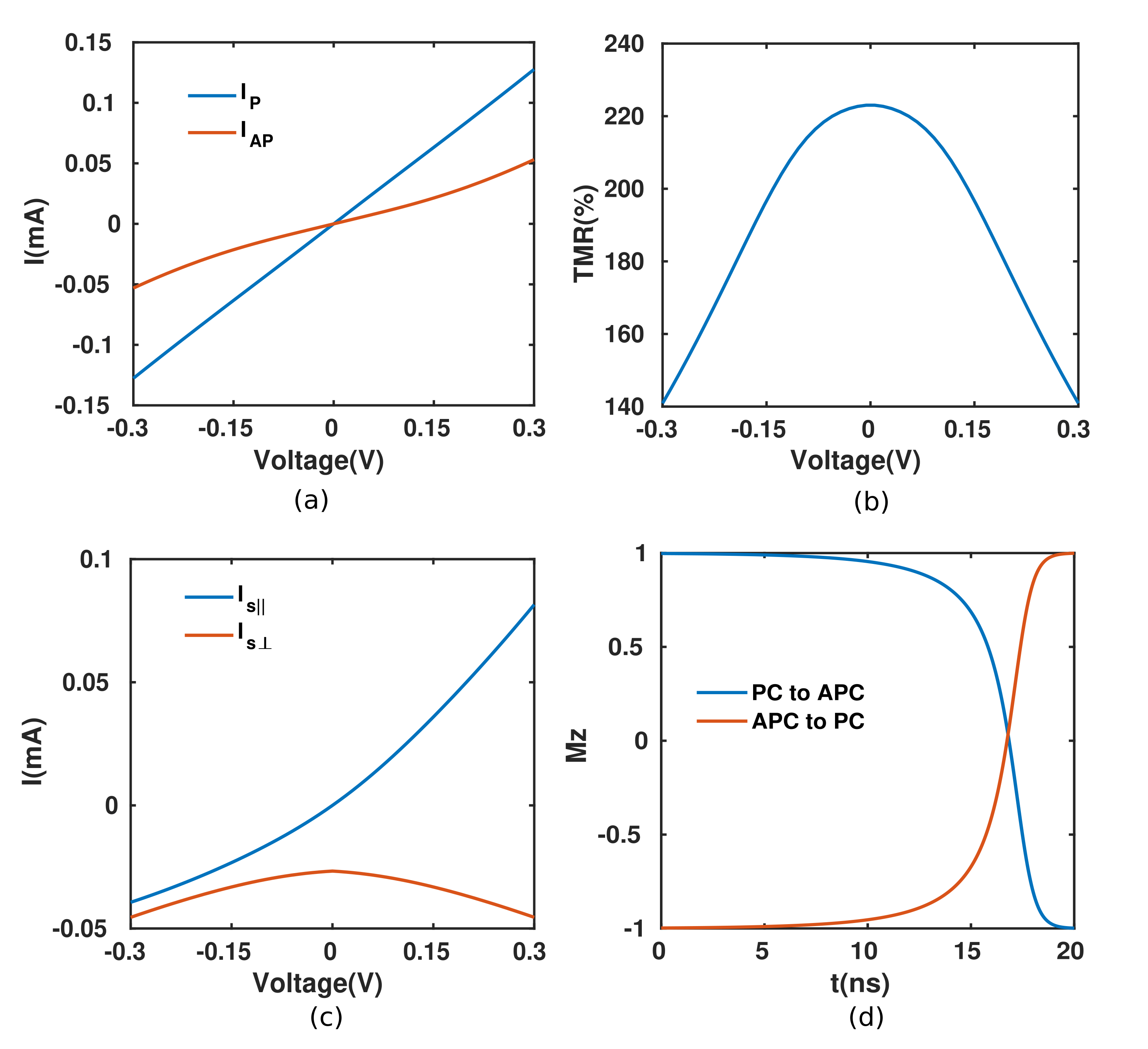
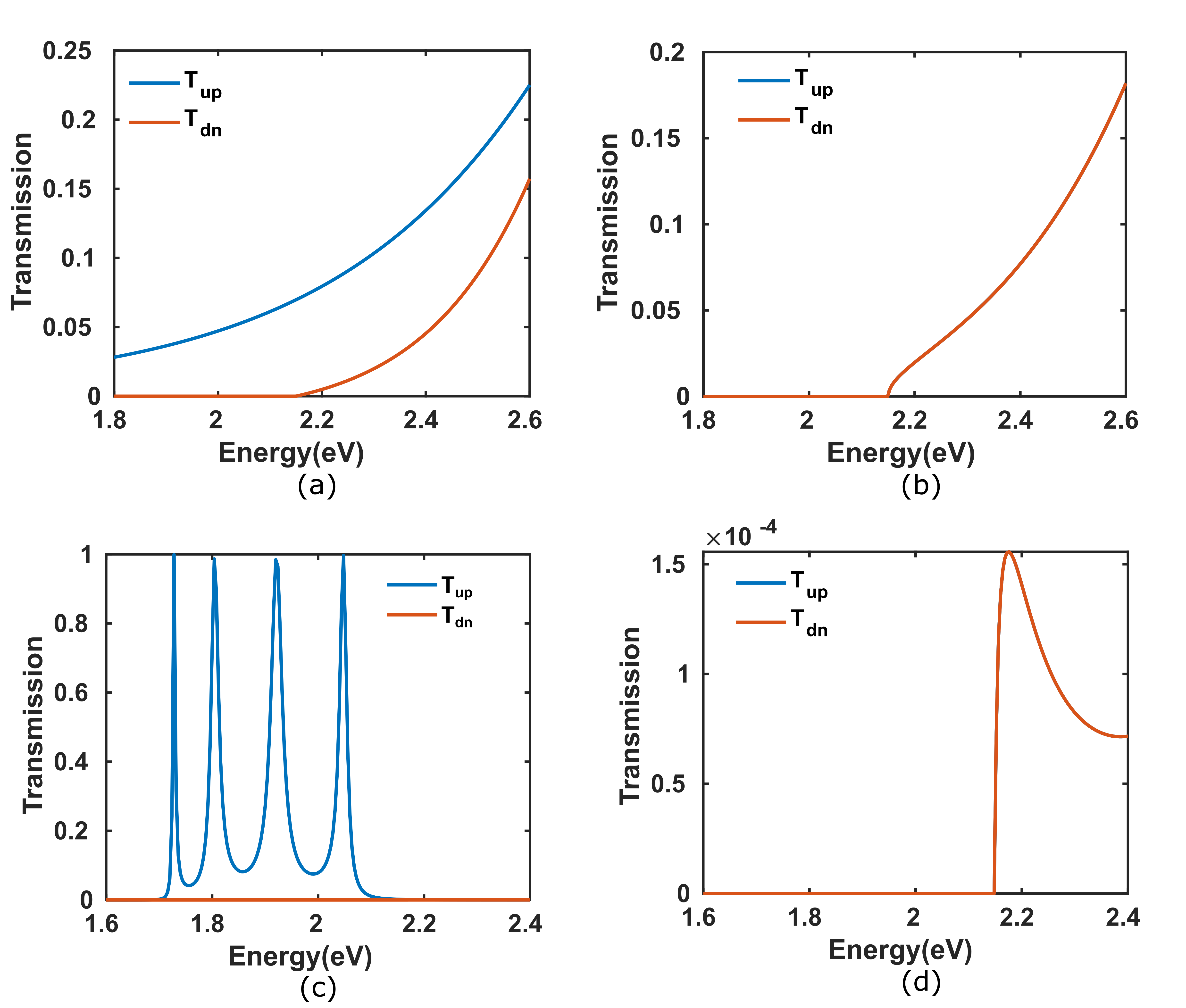
The device consists of an MgO barrier of nm thickness sandwiched between fixed and free FMs. The band diagram of the device is shown in Fig. 2(a). We show the I-V characteristics of the device in the PC and the APC in Fig. 7(a). The maximum TMR(%) provided by the tri-layer MTJ is 240%(Fig. 7(b)). Figure. 7(d) illustrates the STT-switching of the free layer from the APC to PC and the PC to APC at switching-bias of 60 mV and -74 mV, respectively(see Appendix: A). The difference in magnitude of the and originates from the asymmetrical relationship of the device as shown in Fig. 7(c). The TMR and spin current of the trilayer MTJ can be reasoned out from spin selective transmission spectra of the PC (see Fig. 20(a)) and the APC (see Fig. 20(b)) enabled by physics of single barrier tunneling.
III.2 Device characteristics of Linear Width based Nu-SLTJ (LW-SLTJ)
To construct the linear width(LW) based Nu-SLTJ shown in Fig. 3(a), we consider the width of n-th() barrier as
where nm and n=0,1,2. Here represents the central barrier, represents the two neighbour barriers of the central barrier, and represents the two terminal barriers.

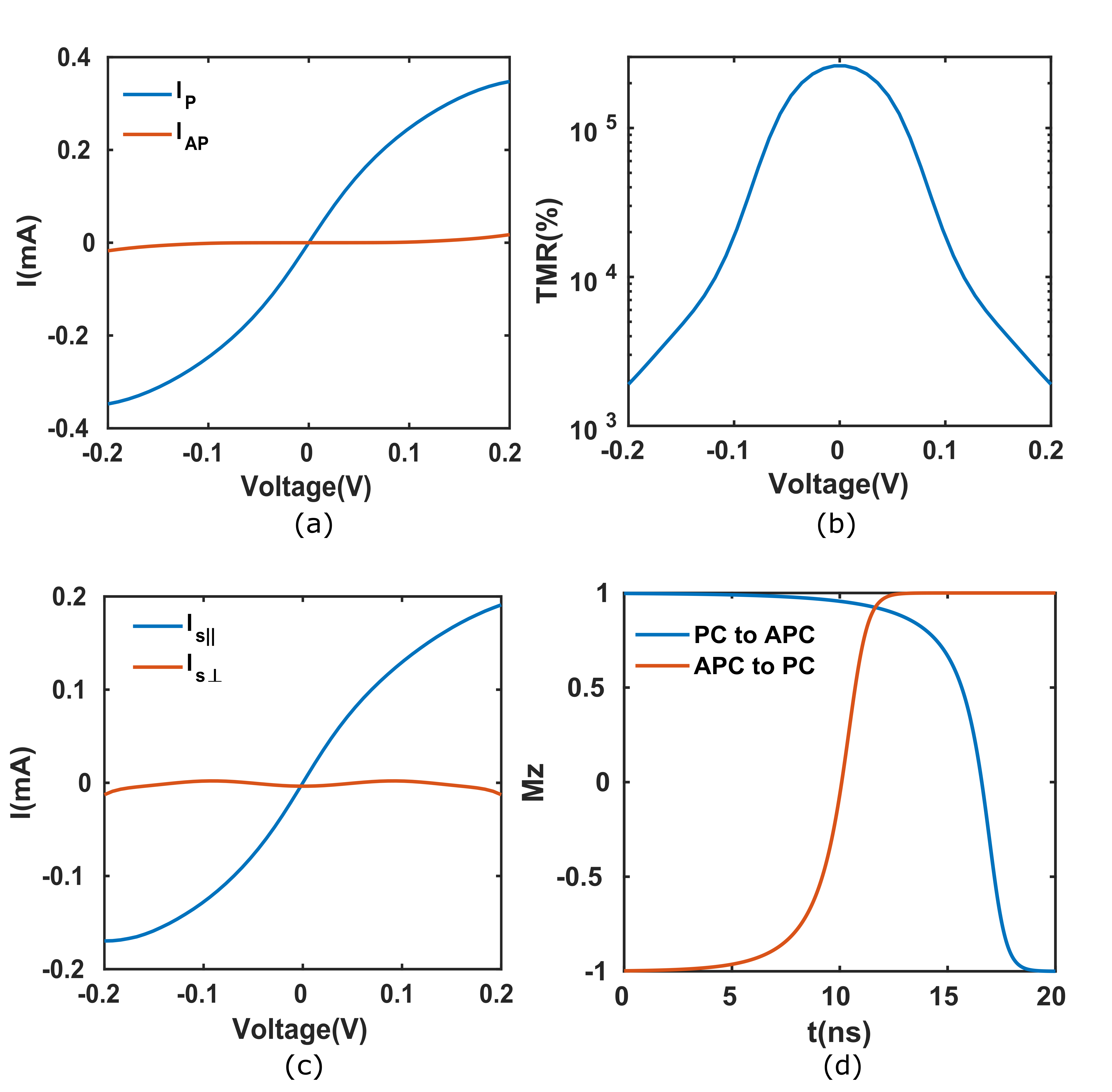
In Fig. 8(a) we present the I-V characteristics of the LW-SLTJ in the PC and the APC. The maximum TMR(%) provided by the device is %. Figure 8(d) shows the STT-switching of the free layer from the PC to APC and the APC to PC with SBPC→APC and SBAPC→PC of -7.4 mV and 7.4 mV, respectively. Unlike the trilayer MTJ, the -V characteristics of the LW-SLTJ is nearly symmetrical around 0V(Fig. 8(c)). Hence the magnitude of switching biases remains the same in both the cases. The sizable ratio of the LW-SLTJ enabled transmissions in the PC(Fig.19(a)) and APC(Fig.19(b)) provides to a monumental enhancement in the TMR(%) as shown in Fig. 8(b). Furthermore, the broad-band spin filtering exhibited by the LW-SLTJ device provides a sizable Is|| which reduces the switching bias substantially, thereby yielding the largest SSB of 9.05(see Tab. 1).
III.3 Device characteristics of Gaussian Width based Nu-SLTJ (GW-SLTJ)
We characterize the thickness of the n-th barrier() in the Gaussian width(GW) based Nu-SLTJ in such a way that
| (13) |
where nm and =0,1,2. The band diagram of the device is presented in Fig. 3(b). In Fig 9(a), we present the I-V characteristics of the GW-SLTJ in the PC and the APC.

The maximum TMR(%) yielded by the device is %(Fig. 9(b)). Similar to the LW-SLTJ, the -V characteristics of the GW-SLTJ is nearly symmetrical around 0V(Fig. 9(c)). Therefore the magnitudes of the SBPC→APC and SBAPC→PC remain the same. In Fig. 9(d) we present the STT-switching of the free layer in the GW-SLTJ for Is||=0.0127 mA. The applied voltages for the PC to APC and the APC to PC switching are -8.88 mV and 8.88 mV, respectively. Therefore, the SSB achieved in this case is 7.61, the 3rd largest among all the Nu-SLTJs(see Tab. 1). Similar to the LW-SLTJ, the significant enhancement in the TMR(%) and Is|| that we accomplish via GW-SLTJ can be rationalized in light of the spin selective broad-band filtering offered by the GW-SLTJ as shown in Figs. 19(c)&(d).
III.4 Device characteristics of Lorentzian Width based Nu-SLTJ(LRW-SLTJ)
The Lorentzian-width(LRW) based Nu-SLTJ is engineered in such a way that the width of n-th barrier() is given by
where nm and =2. We present the band diagram of the device in Fig. 3(c).
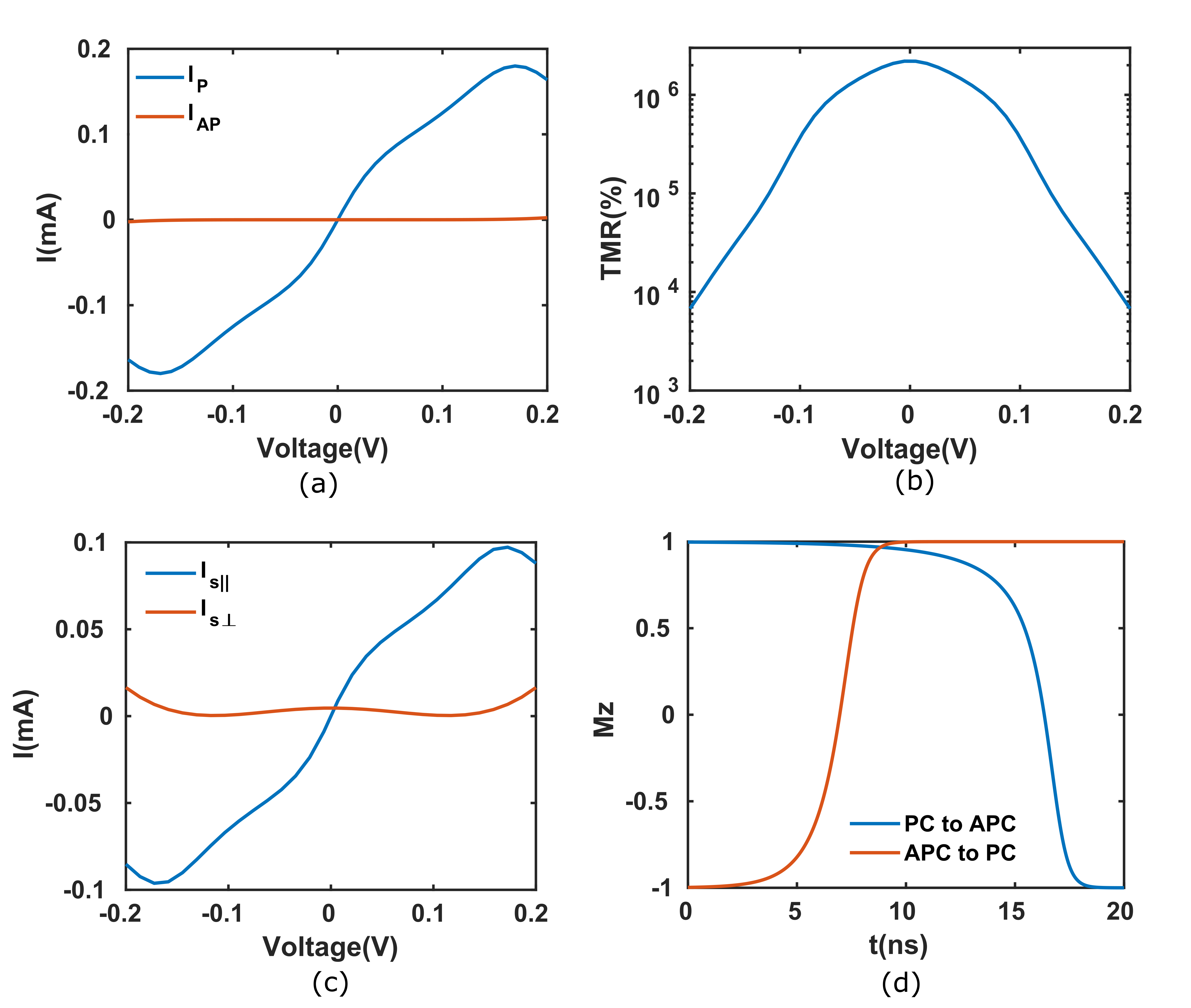
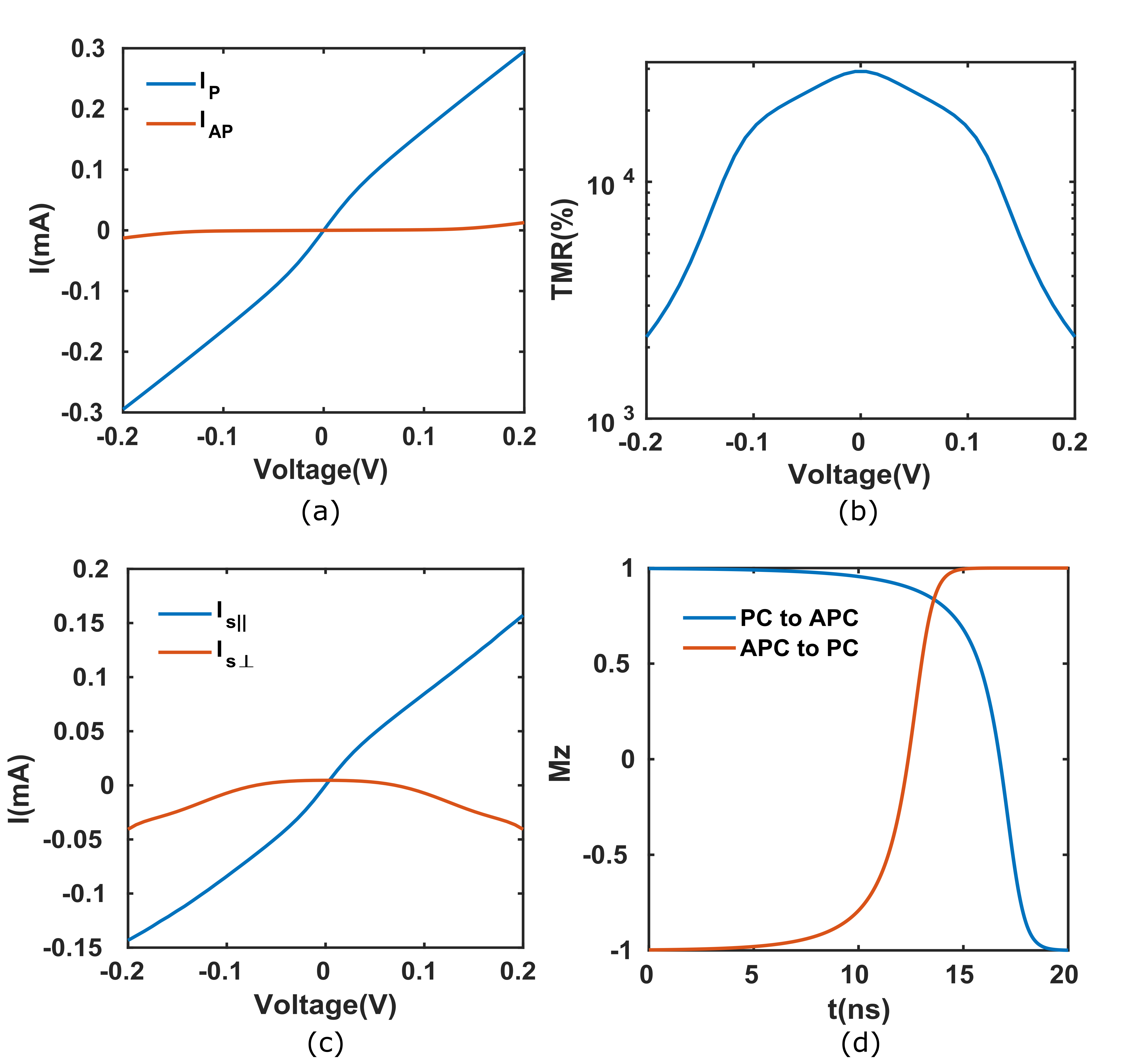
Figure. 10(a) shows the I-V characteristics of the LRW-SLTJ in the PC and the APC. The maximum TMR(%) obtained for this device is 2.19(%)(Fig. 10(b)). We present the variation of the Is|| and Is⟂ with the applied voltage in Fig. 10(c). The switching dynamics of free FM in the SLTJ is presented in Fig.10(d) with the SBAPC→PC and SBPC→APCof -11.7 mV and 11.7 mV, respectively. The LRW-SLTJ provides the 5th largest SSB with 5.73 (see Tab. 1). The superiority of the performance indices in terms of the TMR(%) and the Is|| that we realize through the LRW-SLTJ can be reasoned out on the basis of the heterostructure enabled broad-band spin filtering in the PC and APC as shown in Figs. 19(e)&(f).
III.5 Device characteristics of the Pöschl-Teller Width based Nu-SLTJ(PW-SLTJ)
The Pöschl-Teller width based Nu-SLTJ is constructed in such a way that the thickness
of n-th barrier is given by
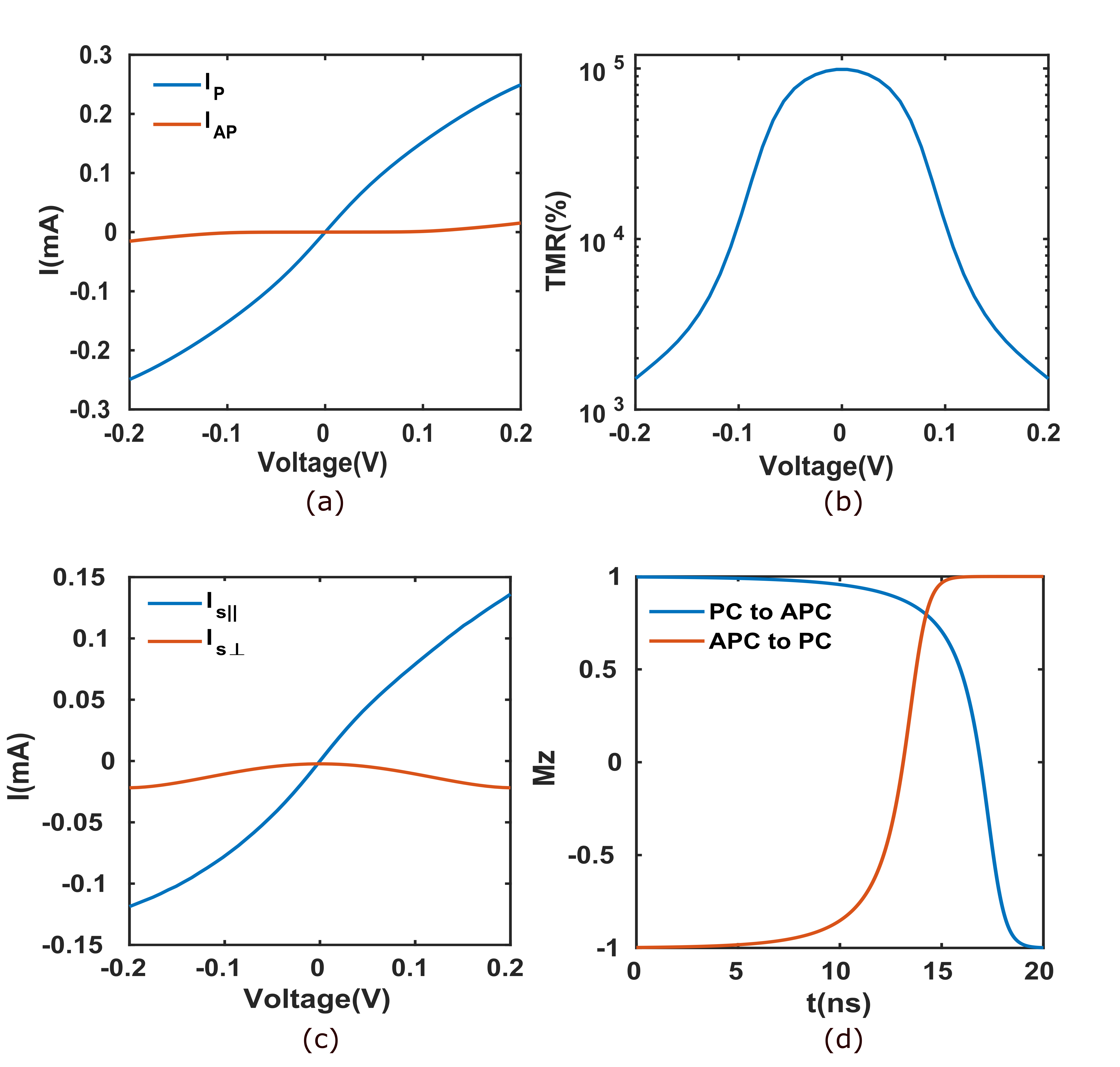
where is 0.6 nm and . The band diagram of the device is shown in Fig. 3(d). In Fig. 11(a) we present the I-V characteristics of the PW-SLTJ in the PC and the APC. The maximum TMR(%) offered by the device is nearly (%). Fig. 11(d) depicts the STT-switching of the free layer from the PC to APC and the APC to PC with the and of -7.75 mV and 7.75 mV, respectively. Hence, the SSB obtained in this case is 8.7(see Tab. 1), the second largest after the LW-SLTJ. The broad-band spin filtering in the PW-SLTJ(see Fig. 19(g)(h)) enables the device to accomplish a remarkable enhancement in the TMR(%) and the Is|| as shown in Fig. 11(b) and 11(c).
III.6 Device characteristics of the Linear Height based Nu-SLTJ(LH-SLTJ)
Along with different width profiles, the Nu-SLTJs with different height profiles also substantiate their worth as potential candidates for high-performance MTJs. Hence, in the subsequent subsections, we present the height-based analogues of the above-mentioned heterostructures geared towards broad-band spin filtering.
At first we devise the Linear height(LH) based Nu-SLTJ as shown in Fig. 4(a), where the scattering potential of the n-th barrier() is given by
with eV representing the central barrier, eV representing the two neighbour barriers of the central barrier, and eV representing the two terminal barriers. We have used MgO to implement the central barrier, and the rest of the barriers are realized by stoichiometrically substituted MgxZn1-xO where is substituted in accordance to design the respective scattering potentials.
In Fig. 12(a), we present the I-V characteristics of the LHSLTJ in the PC and the APC. The maximum TMR(%) provided by the device is approximately (%)(Fig. 12(b)). Figure. 12(d) depicts the switching dynamics of the free layer with the SBPC→APC and SBAPC→PC of -11.6 mV and 11.6 mV, respectively. Therefore, the LH-SLTJ provides an SSB of 5.8, the 4th largest among all the NU-SLTJs(see Tab. 1). Similar to the W-SLTJs, the ratio of transmissions in the PC (Fig. 21(a)) and APC (Fig. 21(b)) is the cornerstone of the towering TMR(%) we accomplish via LH-SLTJ. In addition to this, the large Is|| is attributed to the LH-SLTJ enabled spin-selective broad-band transmission as shown in Fig. 12(c).
III.7 Device characteristics of the Gaussian Height based Nu-SLTJ(GH-SLTJ)
To realize the Gaussian height(GH) based Nu-SLTJ shown in Fig. 4(b), we engineer
the scattering potential () of the n-th barrier in such a way that
where eV and n=0,1,2.
Figure.13(a) depicts the I-V characteristics of GH-SLTJ in the PC and the APC. The maximum TMR(%) we notice in this case is nearly (%)(Fig. 13(b)). In Fig.13(c) we present the variation of the Is|| and Is⟂ with applied voltage. Fig.13(d) describes The STT-switching of the free layer in the GH-SLTJ where the applied voltages for the PC to APC and the APC to PC switching are -13.64 mV and 13.64 mV, respectively. The SSB observed in this case is the 7th largest with 4.9(see Tab. 1). The significant improvement in the TMR(%) and Is|| we achieve via GH-SLTJ can be elucidated in light of the heterostructute enabled broad-band spin filtering demonstrated by Figs. 21(c)(d).
III.8 Device characteristics of the Nu-SLTJ with Lorentzian Height Profile(LRH-SLTJ)
We now advance to engineer the Lorentzian height(LRH) based Nu-SLTJ shown in Fig. 4(c), where the scattering potential() of the n-th barrier

in terms of the central barrier is given by
with , eV and n=0,1,2.
In Fig. 14(a), we present the I-V characteristics of the LRHSLTJ in the PC and the APC. The maximum TMR(%) we observe in this case is close to (%)(Fig. 14(b)). Figure. 14(d) describes the switching dynamics of the free layer with the SBPC→APC and SBAPC→PC of -12.3 mV and 12.3 mV, respectively. Therefore, the LRH-SLTJ yields the 6th largest SSB with 5.4(see Tab. 1). The momentus enhancement in the TMR(%) and Is||(Fig. 14(c)) in the LRH-SLTJ can be reasoned out on the basis of the spin selective broad-band filtering demonstrated in Figs. 21(e)(f).
III.9 Device Characteristics of the Nu-SLTJ with Pöscl-Teller Height Profile(PH-SLTJ)
To devise the Pöscl Teller height based Nu-SLTJ shown in Fig. 4, we consider the scattering potential() of the n-th barrier() as

where eV and n=0,1,2.
In Fig. 15(a), we present the I-V characteristics of the PH-SLTJ in the PC and the APC. The maximum TMR(%) provided by the device is nearly %(Fig. 15(b)). The variation of Is|| and Is⟂ with the applied voltage is plotted in Fig. 15(c). Figure 15(d) shows the STT-switching of the free layer from the PC to APC and the APC to PC with SBPC→APC and SBAPC→PC of -15 mV and 15 mV, respectively. Thus, the PH-SLTJ provides the least SSB of 4.5(see Tab. 1). The large Is|| and the towering TMR(%) we get to witness in the device can be explained on the basis of the spin-selective broad-band transmissions in the PC and the APC as shown in Figs. 21(g)(h).
IV Performance of the Nu-SLTJs at higher voltages
Another significant aspect of the work regarding the Nu-SLTJs encircles their performance indices at higher voltages.
| Type of Device | TMR(%)Peak | SBPC→APC(mV) | SBAPC→PC(mV) | SSB | VP(V) | TMR(%) | I(mA) | I(mA) | tFS(ps) |
|---|---|---|---|---|---|---|---|---|---|
| MTJ | 240 | -74 | 60 | 1 | - | - | - | - | - |
| R-SLTJ | 1.44 | -20.4 | 20.4 | 3.28 | 0.24 | 6.24 | 0.103 | 0.17 | 1061 |
| LW-SLTJ | 1.01 | -7.4 | 7.4 | 9.05 | 0.3 | 4.06 | 0.3 | 0.47 | 380 |
| GW-SLTJ | 9.01 | -8.88 | 8.88 | 7.61 | 0.19 | 4.7 | 0.13 | 0.25 | 882 |
| LRW-SLTJ | 2.19 | -11.7 | 11.7 | 5.73 | 0.18 | 1.53 | 0.1 | 0.18 | 1158 |
| PW-SLTJ | 2.61 | -7.75 | 7.75 | 8.7 | 0.22 | 1.24 | 0.2 | 0.35 | 563 |
| LH-SLTJ | 2.9 | -11.6 | 11.6 | 5.8 | 0.43 | 3.18 | 0.33 | 0.49 | 355 |
| GH-SLTJ | 9.87 | -13.64 | 13.64 | 4.9 | 0.31 | 5 | 0.19 | 0.3 | 621 |
| LRH-SLTJ | 7.13 | -12.3 | 12.3 | 5.4 | 0.36 | 4 | 0.22 | 0.35 | 508 |
| PH-SLTJ | 1.16 | -15 | 15 | 4.5 | 0.29 | 5.6 | 0.16 | 0.26 | 672 |
| ARSLMTJSharma et al. (2021) | 3 | -12 | 12 | 5.6 | 0.088 | 9.8 | 0.06 | 0.9 | 1996 |
Hitherto, the engineering of a robust TMR(%) with the applied bias has appeared to be a major challenge in the novel literatureSharma et al. (2018b) that reverberates while designing the Nu-SLTJs as well. Nevertheless, we demonstrate that the introduction of superlattices can accomplish a decent TMR(%) at a higher voltage and also explore the maximum achievable Is|| via various Nu-SLTJs to perform faster switching.

In the first place, we present a qualitative overview of the current flow through an Nu-SLTJ on the application of an applied bias, governed by the areas of the transmissions in the PC(APC) and APC(AAPC). To calculate the current for a specific voltage, we multiply the quantity with the transmission , where the and represent the Fermi distribution functions of the fixed and free FMs, respectively. Along with an increase in the voltage across an Nu-SLTJ, the difference between the and goes up, resulting a greater leeway for tunneling of the electrons that leads to an upsurge in the current conduction. Besides, furtherance in the voltage after a certain point fails to engender an increment in the current flow. This can be ascribed to the bandpass nature of the transmission that inhibits any additional area of the transmission() from falling within the Fermi window(FW) beyond an instance when the FW engulfs significant . Moreover, as the magnitude of the applied voltage is increased even further, the transmission spectrum of a typical Nu-SLTJ becomes tapered. This results in a reduction in the current conduction that compels all the Nu-SLTJs to exhibit negative differential resistance(NDR) beyond a specific voltage().
We present the high-voltage characteristics of various Nu-SLTJs in Fig. 16 and show the variation of the TMR(%), Is|| and the IP while varying the applied voltage from 0.01 V to 0.6 V. We exclude the point at V=0, where the TMR of the devices becomes immeasurable owing to the zeroed IP and IAP. In Fig. 16(a),(b),(c)(d) we show that the TMR of both the H-SLTJs and the W-SLTJs exhibits a large variation with respect to the applied bias alongside an NDR of the IP-V characteristics after . Interestingly, after reaching the peak, the decline in the Is|| of the H-SLTJs as shown in Fig. 16(e)(f) becomes nearly insignificant, thereby providing grist to an idea for utilizing this behavior to realize a device that produces invariable Is|| with an applied voltage.
The deterioration in the ratio of APC and AAPC quenches the TMR(%) of an orthodox MTJ at a higher voltage. For instance, the trilayer MTJ we present in this work offers a TMR(%) of 220% and 140% at an applied voltage of 10 mV and 300 mV as shown in Fig. 7(b). We stumble upon a similar problem while engineering the Nu-SLTJs as well. Yet, the heterostructure-enabled broad-band spin filtering inhibits the TMR(%) from falling below 103-104(%) while the applied bias ranges from -0.2V to 0.2V. This provides a decent solution regarding the sensitivity of the MTJs within this range. Another question, that may lie dormant is the importance of the TMR(%) at a higher voltage while the switching biases of all the SLTJs lie fairly below 50 mV, is answered by highlighting the applicability of an MTJ in the STNOs. A high TMR(%) at VP offers a bigger difference between the IP and IAP, which ensures a surge in the microwave output power. Therefore the Nu-SLTJs, while providing a far superior TMR(%) and IP compared to an MTJ, emerge as more suitable alternatives in order to design large frequency STNOs with high microwave output powerSharma et al. (2017). Furthermore, we can infer from Tab. 1 that the LW-SLTJ provides an IP of 0.47 mA at the VP along with a TMR(%) of 4.06(%) which entitles the device as a much-coveted candidate for the aforementioned application.
V Comparison of the Performance Indices of the Various Nu-SLTJs
In this section, we discuss the performance indices of the various SLTJs presented in Tab. 1 and carry out a comparative study in reference to the transmission profiles described in Appendix B.
We attribute the monumental TMR(%) profiles accomplished via different heterostructures to the towering ratio of the transmissions in the PC() and APC(TAPC), and elucidate the significant enhancement in the Is|| by the spin selective nature of the broad-band TPC(see Appendix B).
Figure. 19 exemplifies that the LW-SLTJ yields the largest TPC and hence offers a sizeable Is|| that leads to the highest SSB (see Tab. 1) among all the Nu-SLTJs. Thereafter, the PW-SLTJ, GW-SLTJ and LRW-SLTJ comprise the list of the W-SLTJs in the descending order with reference to the APC as shown in Fig. 19. A similar order of the Is|| and SSB of the respective W-SLTJs corroborates the potential impact of the APC on the Slonczewski term(Is||). We also get to witness an impressive consistency in the order of the TMR(%) with the ratio of the APC and AAPC while analysing the relative performances of the various W-SLTJs. Fig. 19 conveys the LRW-SLTJ to possess the largest APC/ AAPC which enables the device to exhibit the tallest TMR(%). Interestingly, the ascending order of the W-SLTJs with respect to the Is|| constitutes the descending order with reference to the TMR(%).
Akin to the W-SLTJs, the heterostructure-enabled spin-selective transmissions play a significant role in governing the performance indices of the H-SLTJs as well. The LH-SLTJ, LRH-SLTJ, GH-SLTJ, and PH-SLTJ comprise the descending order of the H-SLTJs with respect to the APC as shown in Fig. 21. The Is|| we observe in these devices are congruent with their transmission spectra. For instance, the GH-SLTJ yields an exacerbated TPC compared to the LH-SLTJ resulting in a decimated Is||. In addition to this, we also find the variation in the TMR(%) to be proportional with the ratio of APC and AAPC. As we move from the PH-SLTJ to LH-SLTJ, the depression in the value of APC/AAPC reduces the magnitude of the TMR(%). Similar to the W-SLTJs, the order of the H-SLTJs with respect to Is|| and TMR(%) are mutually opposite.
It seems pretty outlandish that despite having a significant TPC, the H-SLTJs tend to fall behind in accomplishing a mammoth SSB, unlike the W-SLTJs. We can ascribe such behaviour to the widespread finger-like profile of the transmissions(see Fig 19 & 21), which reduces effective area within the Fermi window near the switching bias and scales down the steepness of the Is||-V characteristics(see Fig. 16(e)&(f)). On the contrary, although the W-SLTJs exploits their compact TPC to accomplish a sharp slope in the Is||-V curve, the narrower width in the TPC reduces the VP of the devices. As a consequence, the W-SLTJs tend to exhibit the NDR at a lower voltage.
The compendium of Nu-SLTJs devised in this work offer fairly superior performances compared to the anti-reflective superlattice magnetic tunnel junction (ARSLMTJ) Sharma et al. (2021) in many ways. In the first place, we can infer from Tab. 1 that the SSB of the ARSLMTJ is lower than that of all the W-SLTJs, including the LH-SLTJ. Other than that, the maximum I and the TMR that we accomplish via LH-SLTJ and LRW-SLTJ are 600% and 150% higher than same. Importantly, both the W-SLTJs and the H-SLTJs may comprise minimal device structures of three oxide barriers (see Fig. 6) whereas the ARSLMTJ requires minimum five barriers for operation. Thus, the resounding superiority in the performance indices takes place in the Nu-SLTJS along with a reduction in fabrication complexity.
It is worth mentioning that despite having a near box-cart transmission, the ARSLMTJ fails to outperform the W-SLTJs and the LH-SLTJ while providing a lower SSB. This can be accounted to the narrowness of it’s transmission, which reduces the APC engulfed by the FW near the switching bias. These findings do not underpin the necessity of the box-cart-shaped transmissions and establish the importance of a higher APC within the FW as the keystone for accomplishing a lower switching bias. Another dimension that we unveil in this work is the high TMR(%)(Fig. 6(a)(b)) of the R-SLTJ devoid of a box-cart TPC(Fig. 20(c)), which demonstrates the APC/AAPC to be the predominant factor in order to achieve a high TMR(%).
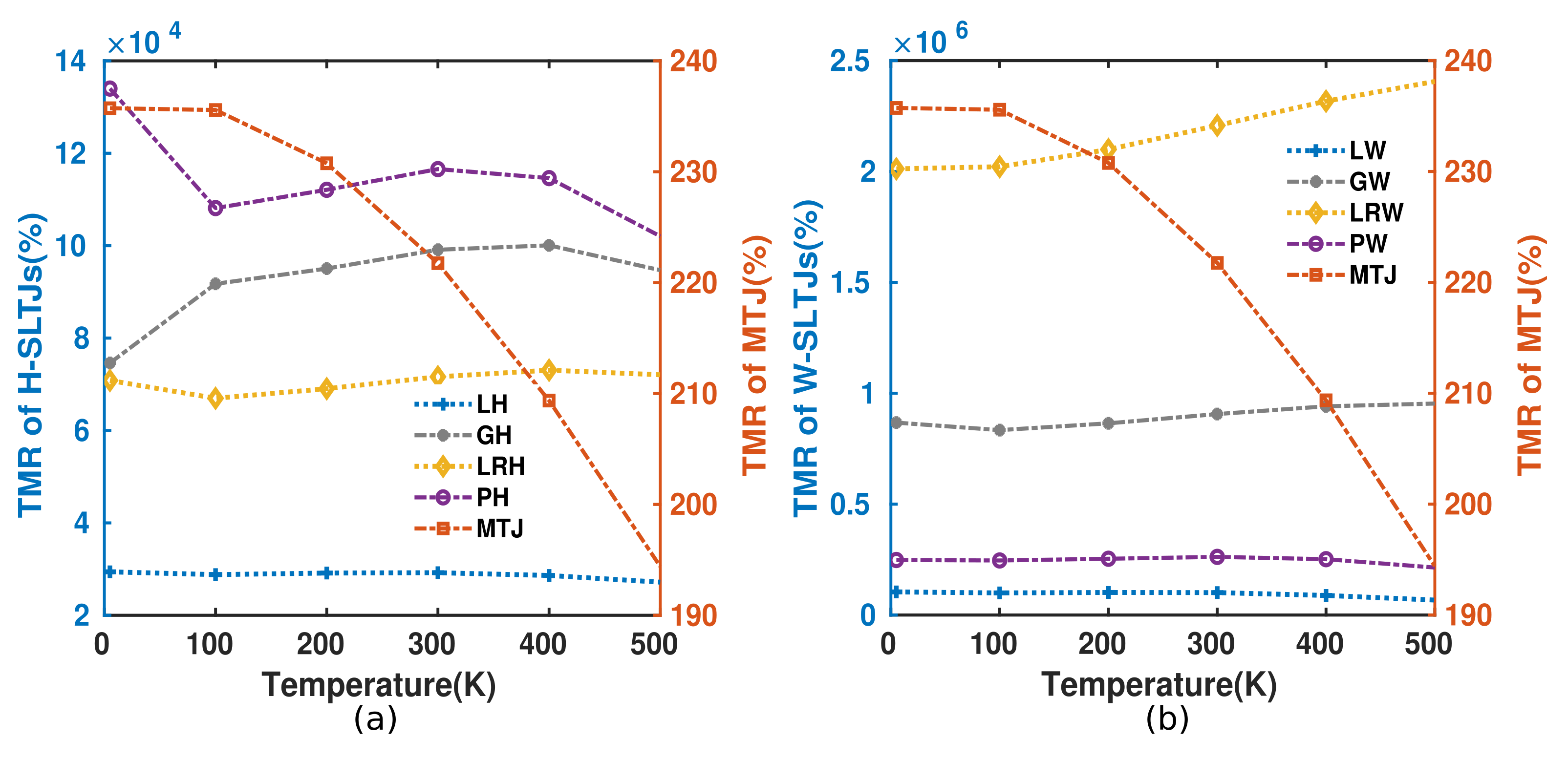
VI Temperature dependence of the TMR of the Nu-SLTJs
The TMR of a CoFeB/MgO/CoFeB-based MTJ has typically been observed to show a monotonic decline with the temperatureZhao et al. (2022); Kou et al. (2006). In Fig. 17 we have shown the TMR dependence of the Nu-SLTJs in reference to a typical MTJ. The decline in the TMR of a trilayer MTJ can be elucidated by the fact that an increase in the temperature widens the FW, which allows the transmissions at higher energies to get indulged in electron transport. Unfortunately, as we move towards higher energies, the ratio of the APC/AAPC gets reduced(Fig. 20(a)), which in turn declines the TMR%. Although earlier works have ascribed the TMR roll-off with temperature to the magnonsZhao et al. (2022); Drewello et al. (2008); Wang et al. (2015); Cao et al. (2019), the same can also be explained by the analysis of the spin-dependent transmission spectra within the FW. The TMR of the Nu-SLTJs exhibits notable robustness to temperature variations. This can be attributed to the broadband nature of the transmissions, which doesn’t allow the ratio of APC and AAPC at higher energies to head downhill. The non-monotonic behavior of the TMR, we observe in the Nu-SLTJs can be explained on the premise of broadened FW at higher temperatures and the transmission that gets engulfed by it at various transverse modes. The analysis of the TMR rendered by the Nu-SLTJs while subjected to magnon interactionsDrewello et al. (2008) is beyond the scope of this work and shall be addressed in future.
VII Conclusion
Low TMR(%) and high switching biasSharma et al. (2017, 2016, 2018a) are the two foremost drawbacks that gridlock the possibility a typical MTJ to become a superior alternative for state-of-the-art storage devices. This study explores the broad-band spin filtering in various Nu-SLTJs that manifests an appreciable enhancement in the TMR and a significant SSB, while endowing the LW-SLTJ with the best TMR(%)- trade-off(TMR(%)105, SSB9.05 and t ps). Since the Nu-SLTJs accomplish a fast STT-switching in the order of a few hundreds of picoseconds, they successfully address the shortcoming of non-deterministic switching in the SOT devices while keeping up with the speedMeo et al. (2022); Prenat et al. (2015). We unveil that a large and a high APC/AAPC within the FW overrides the necessity for the box-cart shape of a transmission in order to obtain a low switching bias and a high TMR(%). Apart from that, we anticipate the Nu-SLTJs devised to find possible applications in the STNOs due to their large IP and considerable TMR(%) at VP. Moreover, we foresee the recent development of double metallic quantum well-based MTJsTao et al. (2019) to add further fuel in the investigation of heterostructure-based memory devices. Finally, we conclude the theoretical analysis of Nu-SLTJs with lower switching bias and high TMR(%) proposed in this article to hopefully pave the avenues for cutting-edge heterostructure-based magnetic tunnel junctions.
Data availability statement
The data that support the findings of this study are available upon reasonable request from the authors.
Appendix A Switching of the free layer
This section deals with the STT-switching of the free FM in the LW-SLTJ, as shown in Fig. 18.
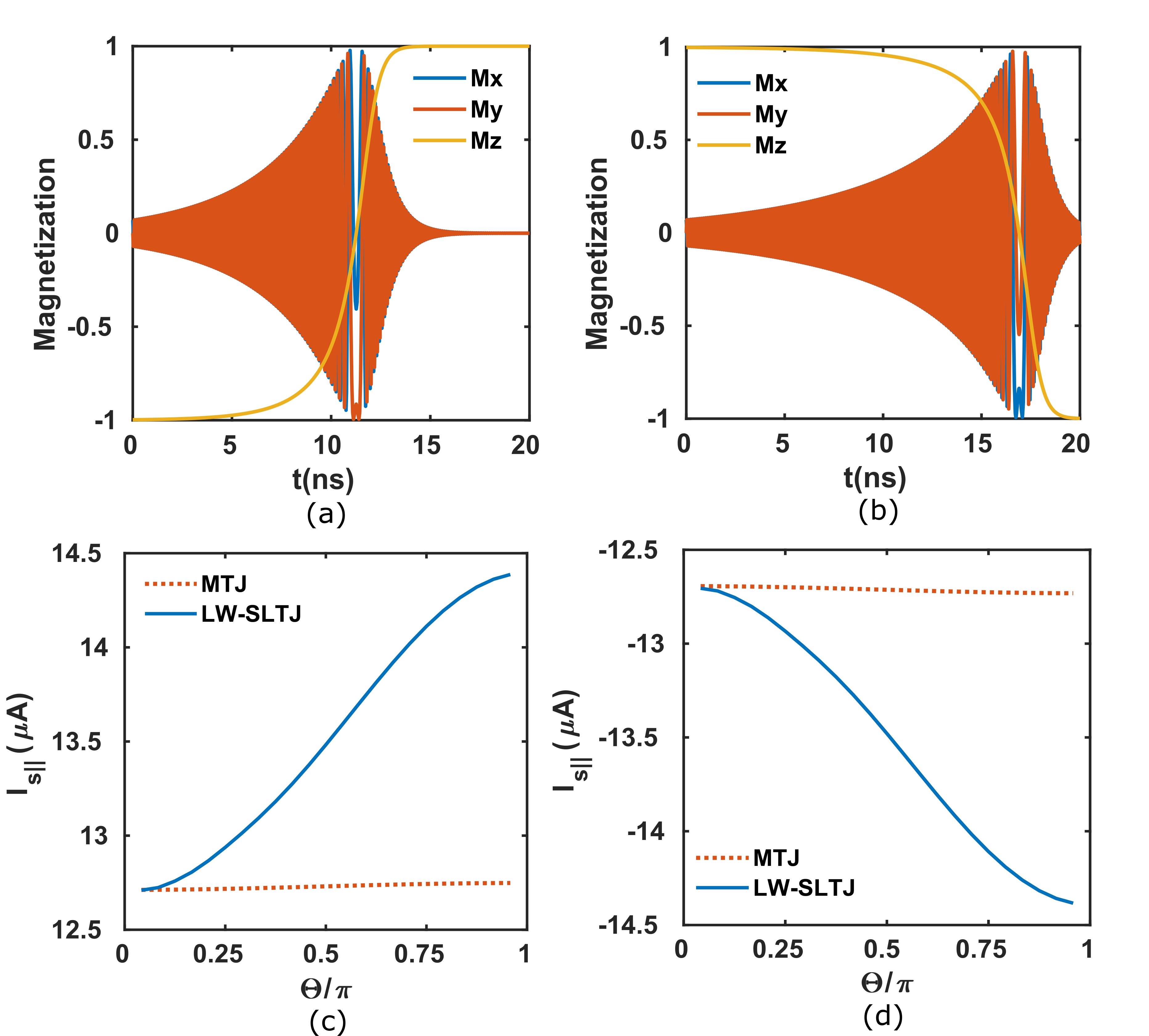
The analysis of the switching dynamics involves the self-consistent coupling of the NEGF formalism with the LLGS equation described in Fig. 5. As the applied Is|| and the magnetization of the free FM resides in the same direction at equilibrium, it is necessary to impart a slight misalignment in the magnetization to produce a non-zero torqueMeo et al. (2022). Since it is not possible to switch the free FM from either 0∘ or 180∘ for the above-mentioned reasons, we assume the relative angle between the magnetization of the free and the fixed FM() as 4∘ and 176∘ in the PC and the APC, respectively. Apart from that, a switching current near the Is||,c induces an insignificant damping to the magnetization. Hence in order to perform a comfortable switching, we apply an Is|| that exceeds the critical current Is||,c by 20%. The desired Is|| is achieved with an and of -7.4 mV and 7.4 mV, respectively. In contrast to a typical MTJ, we observe a considerable variation in the Is|| of the LW-SLTJ with respect to the as shown in Fig. 18(c)(d). Therefore, the time required for the PC to APC(Fig. 18(a)) and the APC to PC(Fig. 18(b)) switching becomes dissimilar. Analogous to the LW-SLTJ, the Is|| of all the Nu-SLTJs devised in this work exhibit a similar behavior with the .

The magnitude of the and the remains the same for all the Nu-SLTJs due to symmetrical variation of the Is|| with respect to the applied voltage near 0V.
Appendix B Analysis of the Transmission Spectra
The analysis of the transmission spectra provide vivid insights to engineer the heterostructure-based magnetic tunnel junctions.
In order to determine the current through a mesoscopic device such as an MTJ and/or Nu-SLTJ, we multiply the Fermi level difference of the fixed and free FMs
to the transmission and integrate the product over the energy.
Hence, the ratio of the APC and AAPC within the Fermi-window(FW) plays a pivotal role in governing the TMR(%). Apart from that, the up-spin transmission(Tup) in a spin-selective heterostructure heavily dominates its down-spin counterpart(Tdn).
Such compelling spin filtering causes the spin(Iz=Iup-Idn) and the charge current(IP) in the direction to become nearly equal in magnitude. Further, the strong correlation of the Iz with the Slonczewski term (Is||) in the spin selective SLTJs ensures a high IP to eventuate a large Is||. Based on these heuristic arguments, we utilize the TPC to predict the behavior of the Is|| with the applied bias.
We embark on elucidating the spintronic characteristics of various Nu-SLTJs with the TPC and TAPC of both the trilayer MTJ and the regular SLTJ depicted in Fig. 20.
The modest opposite spin transmission shown in Fig. 20(a) declines the spin filtering capability of the trilayer MTJ, which restricts the TMR to a trifling 240% compared to the Nu-SLTJs.
In addition to this, the value of the TPC lies well below 1 within the FW, which exacerbates the APC resulting in a low Is||. On the other hand, despite offering a commendable spin filtering, the R-SLTJ exhibits a finger-like TPC which significantly reduces the APC and thereby yields a feeble Is|| along with a meager SSB. Therefore, we propose the idea of Nu-SLTJs, where the presence of the electronic Bloch states in the neighbourhood of the resonant peaks gives rise to a spin selective broad-band TPC, resulting an admirable Is||.
The broad-band spin filtering is referred to the widened TPC that allows a broad transmission window for the electrons aligned to the FMs in the PC, while the opposite spin transmission is nearly suppressed to zero as shown in Figs. 21,19. Further, the towering ratio of the APC and the AAPC witnessed in the Nu-SLTJs (Figs. 21,19) leads to an ultra-high boost in the TMR(%).
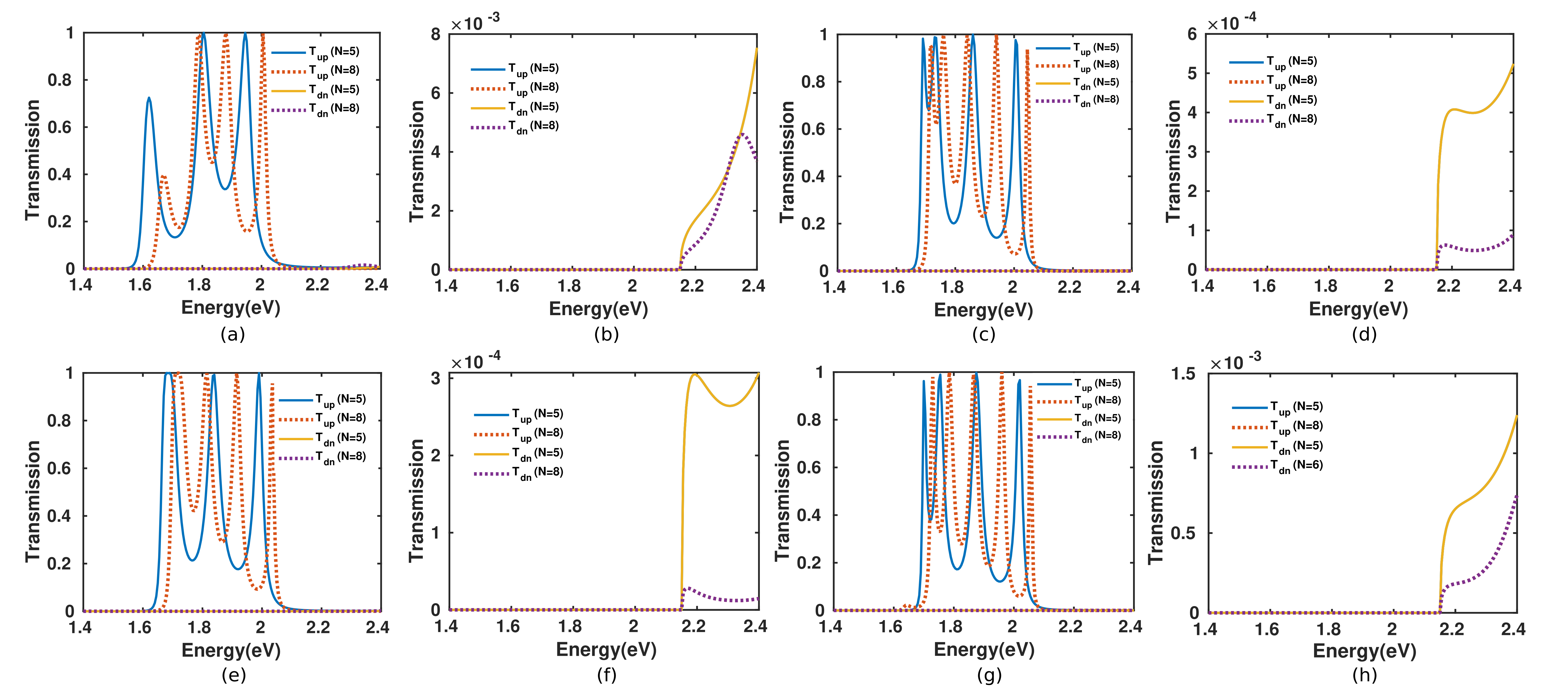
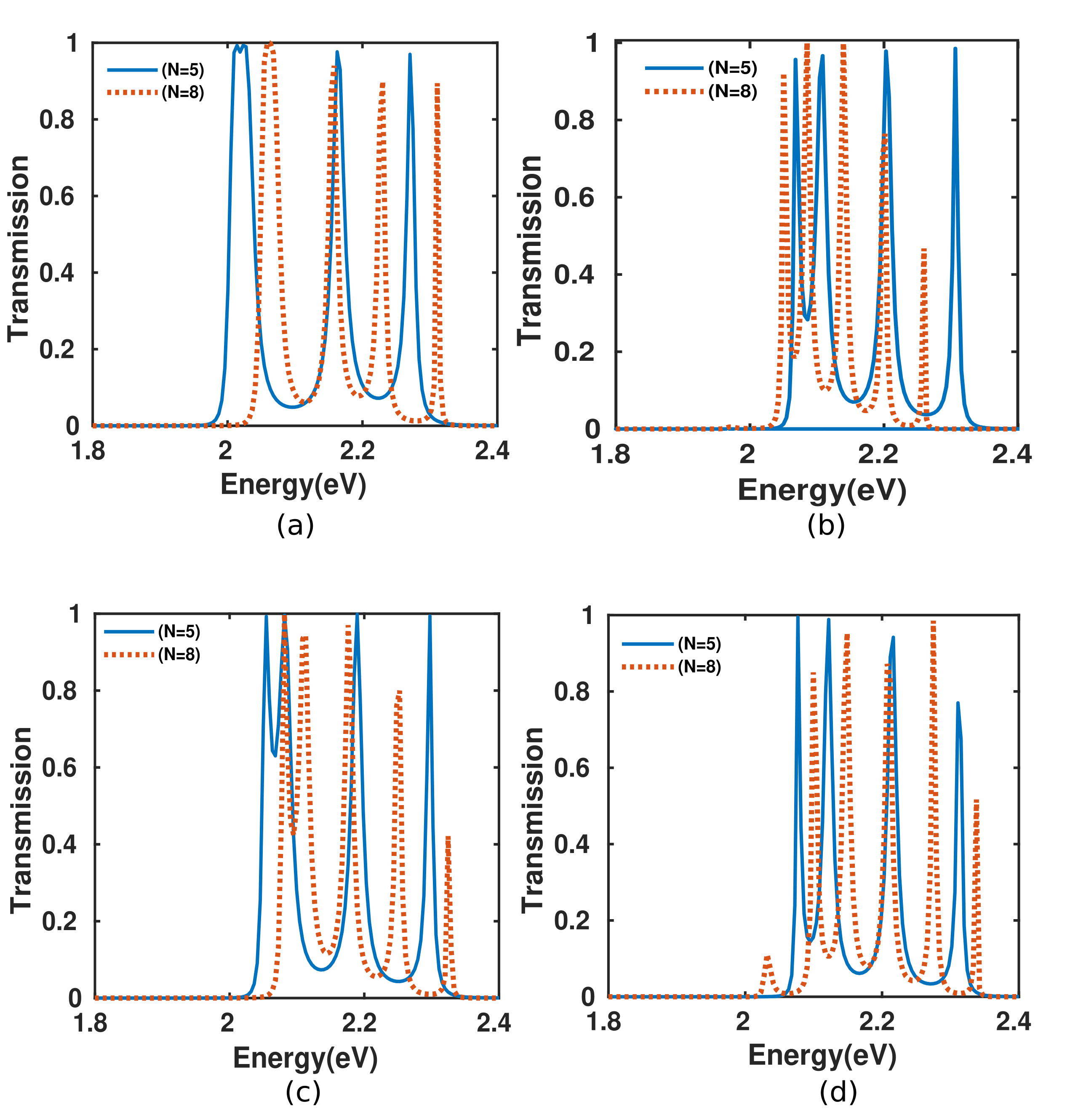
In Fig. 19 we present the transmissions of various W-SLTJs in the PC and the APC for both and =6, where denotes the number barriers comprising the Nu-SLTJs. We find the quantity APC/AAPC and the TPC to elucidate the TMR(%) and the Is|| with a noble consistency. For example, the ratio of the APC and AAPC is able to coherently predict the comparative performance of the TMR(%) in the various W-SLTJs. In addition to this, the relative magnitude of the Is|| corroborates the decisive impact of the TPC on it. Regardless of the width based profiles, the passband in the TPC exhibits remnant oscillations as described in Fig. 19. The TPC of the W-SLTJs display a slight reduction in the area with a surge in the oscillations as the number of barriers are increased from to . Fig. 6(a) shows a steep upsurge in the TMR(%) as we increase the number of barriers from five to six, which can be categorically explained by the sharp dip in the AAPC at as depicted in Fig. 19. At the same time, the comparable Is|| of the LW-SLTJ, GW-SLTJ and the PW-SLTJ at and maintain a precise consistency with their TPC. The considerable reduction in the APC of the LRW-SLTJ from to reverberates in it’s Is|| as well.
In Fig. 21, we show both the TPC and TAPC of all the H-SLTJs for and . We find H-SLTJs display more intricate results in comparison to their width-based counterparts. As we increase the number of the barriers from to , even though the APC of the GH-SLTJ, LRH-SLTJ, and the PH-SLTJ shows an upsurge, the Is|| of the respective devices suffers a decline in contrast to our earlier discussion. This might appear to be a clear dichotomy in the first place but we find the explanation of the bewilderment to be concealed behind the transmissions at higher transverse modes(Et)Sharma et al. (2021).
As we move towards higher Et, the gross bulk of transmission spectra approaches the Fermi window and then eventually moves beyond it. Hence the transmissions at a higher Et around the fermi window plays a more conclusive role in order to determine the Is|| and the TMR(%). In Fig. 22(b),(c)(d) we demonstrate that for Et=0.2 eV the APC of the GH-SLTJ, LRH-SLTJ, and the PH-SLTJ at offers a higher area than that of at , thereby drawing a coherent conclusion in this regard. Apart from that, the increase in the TMR(%) of the H-SLTJs from to is clearly interpretable from Fig. 21.
Appendix C Guidelines for Designing the Nu-SLTJs
In this leg of the article, we describe the impact of modulating

the scattering potential() and width() of the oxide barriers to design the Nu-SLTJs and argue that altering either of them for enhancing the TMR(%) abates the Is|| and vice versa, thereby leading to a novel hypothesis of TMR-Is|| trade-off. In Fig. 23 we present the variation of the TMR and Is|| while varying the minimum thickness of the oxide layer of Nu-SLTJs from 3Åto 9Å. Besides T determines the thickness of all the other barriers in the W-SLTJs, the thickness of each barriers comprising an H-SLTJ is T itself.

The results we obtain from Fig.23 demonstrate that an increase in the T eventuates a near monotonic upsurge of the TMR while manifesting an opposite impact on the Is||. We may attribute such behavioral pattern to the fact that a wider TOX bestows an exacerbated APC resulting a decimated Is||, and at the same time boosts the ratio of the APC and AAPC leading to an increase in the TMR. Analogously, we also perform the analysis regarding the impact of varying scattering potentials() of the oxide barriers on the H-SLTJ and demonstrate the behavior of the Is|| and the TMR to be entangled in a similar fashion.
On the similar lines, we vary the s of the W-SLTJs from 2.4 eV to 3 eV and depict the device characteristics in Fig. 24(a)(b). Since the of the terminal barriers() depends on the central barrier() in the H-SLTJs, lowering the significantly reduces the height of the far below the Fermi energy, thereby sabotaging the spin filtering near the FW.
To avoid this muddle, we keep the variation of the within the limits of 2.7 eV to 3 eV for studying the characteristics of the Is|| and the TMR as shown in Fig 24(c)(d). The results we obtain in this context conveys that an increase in the scattering potential reduces the Is|| and improves the TMR which may again be attributed to the reduction in the APC and improvement in the ratio of the APC and AAPC, respectively.

A qualitative analysis of Fig. 23 and Fig. 24 reveal that the change in the width of the oxide barriers elicit more pronounced impact on the TMR and the Is|| among the SLTJs compared to the variation in the height of the s. Therefore, we may use the variation of the TOX to design the framework of a Nu-SLTJ, while the alteration in the scattering potential might come in handy during the fine-tuning of the performance indices.
It is worthwhile mentioning that the variation of TMR and Is|| shown in Fig. 24(c)(d) establishes the fact that despite a significant variation due to the impact of error in the barrier heights of the H-SLTJs owing to the complexity involved in engineering the height variations for real samples, the TMR remains significantly above whereas the Is|| doesn’t suffer a significant decline. Consequently, the H-SLTJs promise a momentous improvement in the performance indices compared to a typical MTJ, irrespective of the errors in the barrier heights.
The algorithm described in Fig. 25, presents a generic guideline to modulate the performance indices of a typical Nu-SLTJ in order to optimize it for various applications. While using the minimum number of oxide layers to moderate the fabrication complexity, a designer is left to alter only with the thickness of the oxide layers and the scattering potential of the insulators as the UBW is fixed for a particular NM and the width of the quantum well() is decided beforehand for the optimization purposesSharma et al. (2018b). Therefore, by following the algorithm depicted in Fig. 25, one may play around with both the and Tox to meet the target specifications.
References
- Parkin et al. (2004) S. S. Parkin, C. Kaiser, A. Panchula, P. M. Rice, B. Hughes, M. Samant, and S.-H. Yang, Nature materials 3, 862 (2004).
- Berger (1996) L. Berger, Physical Review B 54, 9353 (1996).
- Slonczewski (1996) J. C. Slonczewski, Journal of Magnetism and Magnetic Materials 159, L1 (1996).
- Le Phan et al. (2006) K. Le Phan, H. Boeve, F. Vanhelmont, T. Ikkink, F. De Jong, and H. De Wilde, Sensors and Actuators A: Physical 129, 69 (2006).
- Kanno et al. (2022) A. Kanno, N. Nakasato, M. Oogane, K. Fujiwara, T. Nakano, T. Arimoto, H. Matsuzaki, and Y. Ando, Scientific reports 12, 1 (2022).
- Rudin and Bramble (1997) L. I. Rudin and S. K. Bramble, Investigative Image Processing 2942 (1997).
- Chen et al. (2016) T. Chen, R. K. Dumas, A. Eklund, P. K. Muduli, A. Houshang, A. A. Awad, P. Dürrenfeld, B. G. Malm, A. Rusu, and J. Åkerman, Proceedings of the IEEE 104, 1919 (2016).
- Braganca et al. (2010) P. Braganca, B. Gurney, B. Wilson, J. Katine, S. Maat, and J. Childress, Nanotechnology 21, 235202 (2010).
- Robbes (2006) D. Robbes, Sensors and Actuators A: Physical 129, 86 (2006).
- Krivorotov et al. (2005) I. Krivorotov, N. Emley, J. Sankey, S. Kiselev, D. Ralph, and R. Buhrman, Science 307, 228 (2005).
- Choi et al. (2014) H. S. Choi, S. Y. Kang, S. J. Cho, I.-Y. Oh, M. Shin, H. Park, C. Jang, B.-C. Min, S.-I. Kim, S.-Y. Park, et al., Scientific reports 4, 1 (2014).
- Cheng et al. (2016) R. Cheng, D. Xiao, and A. Brataas, Physical review letters 116, 207603 (2016).
- Bhattacharjee et al. (2018) N. Bhattacharjee, A. Sapozhnik, S. Y. Bodnar, V. Y. Grigorev, S. Y. Agustsson, J. Cao, D. Dominko, M. Obergfell, O. Gomonay, J. Sinova, et al., Physical review letters 120, 237201 (2018).
- Jiang et al. (2004) Y. Jiang, T. Nozaki, S. Abe, T. Ochiai, A. Hirohata, N. Tezuka, and K. Inomata, Nature materials 3, 361 (2004).
- Mangin et al. (2006) S. Mangin, D. Ravelosona, J. Katine, M. Carey, B. Terris, and E. E. Fullerton, Nature materials 5, 210 (2006).
- Diao et al. (2007) Z. Diao, Z. Li, S. Wang, Y. Ding, A. Panchula, E. Chen, L.-C. Wang, and Y. Huai, Journal of Physics: Condensed Matter 19, 165209 (2007).
- Santos et al. (2020) T. S. Santos, G. Mihajlović, N. Smith, J.-L. Li, M. Carey, J. A. Katine, and B. D. Terris, Journal of Applied Physics 128, 113904 (2020).
- Ikeda et al. (2007) S. Ikeda, J. Hayakawa, Y. M. Lee, F. Matsukura, Y. Ohno, T. Hanyu, and H. Ohno, IEEE Transactions on Electron Devices 54, 991 (2007).
- Apalkov et al. (2013) D. Apalkov, A. Khvalkovskiy, S. Watts, V. Nikitin, X. Tang, D. Lottis, K. Moon, X. Luo, E. Chen, A. Ong, et al., ACM Journal on Emerging Technologies in Computing Systems (JETC) 9, 1 (2013).
- Khvalkovskiy et al. (2013) A. Khvalkovskiy, D. Apalkov, S. Watts, R. Chepulskii, R. Beach, A. Ong, X. Tang, A. Driskill-Smith, W. Butler, P. Visscher, et al., Journal of Physics D: Applied Physics 46, 074001 (2013).
- Bhatti et al. (2017) S. Bhatti, R. Sbiaa, A. Hirohata, H. Ohno, S. Fukami, and S. Piramanayagam, Materials Today 20, 530 (2017).
- Prenat et al. (2007) G. Prenat, M. El Baraji, W. Guo, R. Sousa, L. Buda-Prejbeanu, B. Dieny, V. Javerliac, J.-P. Nozieres, W. Zhao, and E. Belhaire, in 2007 14th IEEE international conference on electronics, circuits and systems (IEEE, 2007) pp. 190–193.
- Bonetti et al. (2010) S. Bonetti, V. Tiberkevich, G. Consolo, G. Finocchio, P. Muduli, F. Mancoff, A. Slavin, and J. Åkerman, Physical review letters 105, 217204 (2010).
- Villard et al. (2009) P. Villard, U. Ebels, D. Houssameddine, J. Katine, D. Mauri, B. Delaet, P. Vincent, M.-C. Cyrille, B. Viala, J.-P. Michel, et al., IEEE Journal of solid-state circuits 45, 214 (2009).
- Zeng et al. (2013) Z. Zeng, G. Finocchio, and H. Jiang, Nanoscale 5, 2219 (2013).
- Mizushima et al. (2010) K. Mizushima, K. Kudo, T. Nagasawa, and R. Sato, Journal of Applied Physics 107, 063904 (2010).
- Butler et al. (2001) W. Butler, X.-G. Zhang, T. Schulthess, and J. MacLaren, Physical Review B 63, 054416 (2001).
- Meo et al. (2022) A. Meo, J. Chureemart, R. W. Chantrell, and P. Chureemart, Scientific reports 12, 1 (2022).
- Slaughter et al. (2016) J. Slaughter, K. Nagel, R. Whig, S. Deshpande, S. Aggarwal, M. DeHerrera, J. Janesky, M. Lin, H.-J. Chia, M. Hossain, et al., in 2016 IEEE International Electron Devices Meeting (IEDM) (IEEE, 2016) pp. 21–5.
- Endoh et al. (2020) T. Endoh, H. Honjo, K. Nishioka, and S. Ikeda, in 2020 IEEE Symposium on VLSI Technology (IEEE, 2020) pp. 1–2.
- Byun et al. (2021) J. Byun, D.-H. Kang, and M. Shin, AIP Advances 11, 015035 (2021).
- Sharma et al. (2017) A. Sharma, A. A. Tulapurkar, and B. Muralidharan, Phys. Rev. Applied 8, 064014 (2017).
- Sharma et al. (2016) A. Sharma, A. Tulapurkar, and B. Muralidharan, IEEE Transactions on Electron Devices 63, 4527 (2016).
- Sharma et al. (2018a) A. Sharma, A. A. Tulapurkar, and B. Muralidharan, AIP Advances 8, 055913 (2018a).
- Chen and Hsueh (2014) C. Chen and W. Hsueh, Applied Physics Letters 104, 042405 (2014).
- Chen et al. (2015) C. H. Chen, Y. H. Cheng, and W. J. Hsueh, EPL (Europhysics Letters) 111, 47005 (2015).
- Devaraj and Tarafder (2021) N. Devaraj and K. Tarafder, Physical Review B 103, 165407 (2021).
- Zhang et al. (2022) Y. Zhang, J. Liu, R. Deng, X. Shi, H. Tang, H. Chen, and H. Yuan, RSC advances 12, 28533 (2022).
- Zhao et al. (2018) P. Zhao, J. Li, H. Jin, L. Yu, B. Huang, and D. Ying, Physical Chemistry Chemical Physics 20, 10286 (2018).
- Tao et al. (2019) B. Tao, C. Wan, P. Tang, J. Feng, H. Wei, X. Wang, S. Andrieu, H. Yang, M. Chshiev, X. Devaux, et al., Nano Letters 19, 3019 (2019).
- Bhattacharjee et al. (2016) M. Bhattacharjee, H. Nemade, and D. Bandyopadhyay, in Journal of Physics: Conference Series, Vol. 759 (IOP Publishing, 2016) p. 012051.
- Tseng et al. (2020) P. Tseng, Z.-Y. Chen, and W.-J. Hsueh, New Journal of Physics 22, 093005 (2020).
- Diez et al. (2000) E. Diez, I. Gómez, F. Domınguez-Adame, R. Hey, V. Bellani, and G. Parravicini, Physica E: Low-dimensional Systems and Nanostructures 7, 832 (2000).
- Gómez et al. (1999) I. Gómez, F. Domınguez-Adame, E. Diez, and V. Bellani, Journal of Applied Physics 85, 3916 (1999).
- Sánchez-Arellano et al. (2019) A. Sánchez-Arellano, J. Madrigal-Melchor, and I. Rodríguez-Vargas, Scientific reports 9, 1 (2019).
- Tian et al. (2014) F. Tian, D. Duan, D. Li, C. Chen, X. Sha, Z. Zhao, B. Liu, and T. Cui, Scientific reports 4, 1 (2014).
- Li et al. (2014) D. Li, Q. Ma, S. Wang, R. Ward, T. Hesjedal, X.-G. Zhang, A. Kohn, E. Amsellem, G. Yang, J. Liu, et al., Scientific Reports 4, 1 (2014).
- Sharma et al. (2021) A. Sharma, A. A. Tulapurkar, and B. Muralidharan, Journal of Applied Physics 129, 233901 (2021).
- Sharma et al. (2018b) A. Sharma, A. A. Tulapurkar, and B. Muralidharan, Applied Physics Letters 112, 192404 (2018b).
- Datta (2018) S. Datta, Lessons from Nanoelectronics: A New Perspective on Transport—Part B: Quantum Transport (World Scientific, 2018).
- Ralph and Stiles (2008) D. C. Ralph and M. D. Stiles, Journal of Magnetism and Magnetic Materials 320, 1190 (2008).
- Datta (2005) S. Datta, Quantum transport: atom to transistor (Cambridge university press, 2005).
- Datta (1997) S. Datta, Electronic transport in mesoscopic systems (Cambridge university press, 1997).
- Ralph et al. (2011) D. Ralph, Y.-T. Cui, L. Liu, T. Moriyama, C. Wang, and R. Buhrman, Philosophical Transactions of the Royal Society A: Mathematical, Physical and Engineering Sciences 369, 3617 (2011).
- Tudu and Tiwari (2017) B. Tudu and A. Tiwari, Vacuum 146, 329 (2017).
- Prakash et al. (2017) R. Prakash, B. P. S. Rathore, and D. Kaur, Journal of Alloys and Compounds 726, 693 (2017).
- Ikeda et al. (2010) S. Ikeda, K. Miura, H. Yamamoto, K. Mizunuma, H. Gan, M. Endo, S. Kanai, J. Hayakawa, F. Matsukura, and H. Ohno, Nature materials 9, 721 (2010).
- Miao et al. (2006) G.-X. Miao, K. B. Chetry, A. Gupta, W. H. Butler, K. Tsunekawa, D. Djayaprawira, and G. Xiao, Journal of applied physics 99, 08T305 (2006).
- Datta et al. (2011) D. Datta, B. Behin-Aein, S. Datta, and S. Salahuddin, IEEE Transactions on Nanotechnology 11, 261 (2011).
- Datta (2012) B. Datta, IEEE Transactions on Nanotechnology 11, 261 (2012).
- Yang et al. (2015) S.-H. Yang, K.-S. Ryu, and S. Parkin, Nature nanotechnology 10, 221 (2015).
- Deac et al. (2008) A. M. Deac, A. Fukushima, H. Kubota, H. Maehara, Y. Suzuki, S. Yuasa, Y. Nagamine, K. Tsunekawa, D. D. Djayaprawira, and N. Watanabe, Nature Physics 4, 803 (2008).
- Sato et al. (2014) H. Sato, E. Enobio, M. Yamanouchi, S. Ikeda, S. Fukami, S. Kanai, F. Matsukura, and H. Ohno, Applied Physics Letters 105, 062403 (2014).
- Gajek et al. (2012) M. Gajek, J. Nowak, J. Sun, P. Trouilloud, E. O’sullivan, D. Abraham, M. Gaidis, G. Hu, S. Brown, Y. Zhu, et al., Applied Physics Letters 100, 132408 (2012).
- Zhao et al. (2022) D. Zhao, Y. Wang, J. Shao, Y. Chen, Z. Fu, Q. Xia, S. Wang, X. Li, G. Dong, M. Zhou, et al., AIP Advances 12, 055114 (2022).
- Kou et al. (2006) X. Kou, J. Schmalhorst, A. Thomas, and G. Reiss, Applied physics letters 88, 212115 (2006).
- Drewello et al. (2008) V. Drewello, J. Schmalhorst, A. Thomas, and G. Reiss, Phys. Rev. B 77, 014440 (2008).
- Wang et al. (2015) Y. Wang, H. Cai, L. Naviner, Y. Zhang, J. Klein, and W. Zhao, Microelectronics Reliability 55, 1649 (2015), proceedings of the 26th European Symposium on Reliability of Electron Devices, Failure Physics and Analysis.
- Cao et al. (2019) K. Cao, H. Li, W. Cai, J. Wei, L. Wang, Y. Hu, Q. Jiang, H. Cui, C. Zhao, and W. Zhao, IEEE Transactions on Magnetics 55, 1 (2019).
- Prenat et al. (2015) G. Prenat, K. Jabeur, P. Vanhauwaert, G. Di Pendina, F. Oboril, R. Bishnoi, M. Ebrahimi, N. Lamard, O. Boulle, K. Garello, et al., IEEE Transactions on Multi-Scale Computing Systems 2, 49 (2015).