Present address: ]Hiroshima Synchrotron Radiation Center, Hiroshima University, Higashi-hiroshima, Hiroshima 739-0046, Japan.
Semiconducting Electronic Structure of the Ferromagnetic Spinel
Revealed by Soft-X-Ray Angle-Resolved Photoemission Spectroscopy
Abstract
We study the electronic structure of the ferromagnetic spinel by soft-x-ray angle-resolved photoemission spectroscopy (SX-ARPES) and first-principles calculations. While a theoretical study has predicted that this material is a magnetic Weyl semimetal, SX-ARPES measurements give direct evidence for a semiconducting state in the ferromagnetic phase. Band calculations based on the density functional theory with hybrid functionals reproduce the experimentally determined band gap value, and the calculated band dispersion matches well with ARPES experiments. We conclude that the theoretical prediction of a Weyl semimetal state in underestimates the band gap, and this material is a ferromagnetic semiconductor.
Angle-resolved photoemission spectroscopy (ARPES) is a powerful tool for investigating the electronic structure of solids because ARPES can directly observe band dispersions [1]. By comparing ARPES spectra with ab initio band calculations, it is possible to verify the presence of various emergent electronic properties, such as Weyl points in polar Weyl semimetals [2, 3, 4, 5] and magnetic Weyl semimetals [6, 7]. Density functional theory (DFT) [8, 9] calculations are often used to predict the electronic structure of a material, but DFT calculations are known to underestimate the width of the band gap of solids [10]. The discrepancy between calculations and experiments can be eliminated with the help of hybrid functionals, where model parameters are adjusted to reproduce the experimentally determined materials’ characteristics [11].
Among the materials showing very different characteristics in calculations and experiments, the ferromagnetic spinel (space group , ) [12, 13, 14, 15, 16] is one of the most intriguing. Magnetotransport studies have reported that this material is an insulator [12] or either a - or -type semiconductor [17], depending on crystal growth conditions. Infrared optical measurements have observed a band gap of 0.3–0.8 eV depending on temperature [18, 19, 20]. The proposed - model [21] accounting for direct alllowed transition at the point and the band gap could explain the temperature dependence of electron mass and the anisotropy of the magnetoresistance of -type materials [22]. On the other hand, recent DFT calculations using the generalized gradient approximation (GGA) for the exchange-correlation functional have predicted a semimetallic electronic structure and the presence of magnetic Weyl points near the Fermi level [23]. Their prediction and another study on pyrochlore iridates [24] are two of the earliest works of magnetic Weyl semimetals. Following the magnetic Weyl semimetal proposal, additional support for the Weyl semimetal state was found by the observation of the anomalous Hall effect (AHE) [25]. However, the AHE of has an unconventional temperature dependence [26]. Since then, a theoretical study has suggested that the observed AHE temperature dependence may be extrinsic, caused by scattering, and unrelated to magnetic Weyl semimetals [27]. In addition, another report on the band dispersion of [28] has claimed that the modified Becke-Johnson exchange-correlation functional [29] yields a gapped magnetic semiconductor phase. To the best of our knowledge, the direct observation of the band dispersion by ARPES has been missing, and the real electronic structure of is still under debate.
In this Letter, we report the first observation of the band dispersion of by soft-x-ray (SX) ARPES. We observed only hole bands around the Fermi level and did not find any electron bands crossing them. This result unambiguously indicates that has a semiconducting electronic structure in the ferromagnetic phase, which is consistent with the previously reported transport and optical properties [12, 17, 18, 19]. Our accurate DFT calculations using hybrid functionals could reproduce the semiconducting band dispersion, and the calculated band dispersion agrees well with the experimental results. Our results highlight that a simple comparison of ARPES spectra with DFT calculations has to be handled with care.
Single crystals of were grown by the chemical transport reaction technique using as a carrier agent. The crystal structure was analyzed by powder x-ray diffraction (Supplemental Material Fig. S1 in [30]). We used three single crystals in the experiments; two of them ( and ) were -type, and the other () was -type. Since as-grown crystals usually become -type, the -type crystals were obtained by annealing them in a Hg vapor [17, 15, 33, 34, 35]. A triangular face of a single crystal and the edge of the triangle [Fig. 1(a)] correspond to the plane and the direction, respectively (Supplemental Material Note 2 in [30]). We set the axes so that the axis was parallel to the edge and the axis was perpendicular to the plane [Figs. 1(a) and (b)]. The characteristics of single crystals were examined by transport, magnetic, and infrared transmission analysis (Note 3 in the Supplemental Material [30]). SX- and VUV-ARPES measurements were performed at BL25SU of SPring-8 [36], and supplemental ARPES measurements using vacuum ultraviolet (VUV) light were performed at BL5U of UVSOR, respectively. We used 400–550 eV SX light in SX-ARPES measurements and 60 eV VUV light in VUV-ARPES measurements. The measurement temperature was kept around 50 K. The samples were cleaved in situ in ultrahigh vacuum better than . The cleaved surfaces were later examined by contact-mode atomic force microscopy (AFM) in air. The electronic band structures were calculated from first principles using the Quantum Espresso [37] and Wannier90 [38] packages (Note 3 in the Supplemental Material [30]). The charge density was calculated with the Kohn-Sham equation with the Heyd-Scuseria-Ernzerhof (HSE) 06 exchange-correlation functional [39, 40]. After that, the Kohn-Sham bands were derived with the Wannier interpolation method [41, 42]. The experimentally observed crystal structure was adopted, and spin-orbit coupling was included in the calculations.
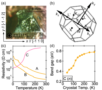
We distinguished - and -types by the temperature dependence of the resistivity [Fig. 1(c)]; -type crystals ( and ) exhibited increasing resistivity at lower temperature while the resistivity of an -type crystal () dropped upon cooling at around [17, 33, 25, 43]. These conductivity types are consistent with the Seebeck coefficient signs determined by a hot-probe method at room temperature. We observed some steps and spikes in the – curves. We think they can be due to the magnetic domain structure reformation with changing the temperature; the anomalous magnetoresistance behavior [Fig. S3(a) in the Supplemental Material [30]] indicates unconventional transport properties at the magnetic domain boundaries. Since the resistivity curve for the -type sample is similar to that of metal, -type has been considered to be a degenerated semiconductor [17, 33]. The magnetic property measurements showed ferromagnetic behavior below [Figs. S3(b) and S3(c) in the Supplemental Material [30]]. The transmittance spectra of -type (crystal ) showed a steplike feature [Fig. S4 in the Supplemental Material [30]]; the transmittance steeply dropped to nearly zero above a threshold, indicating the existence of a band gap. The band gap energy estimated from these spectra [Fig. 1(d)] exhibits a similar temperature dependence to previous studies [18, 19, 20]. Since the previous studies use -type samples to measure the band gap, our measurements of the -type sample clarify that the band gap behavior is independent of the carrier type. All these results are consistent with the previous reports claiming that is a ferromagnetic semiconductor.
Using SX-ARPES, we present conclusive evidence for the semiconducting electronic structure of in the ferromagnetic phase. We could observe band dispersions from all three samples. Figure 2(a) represents the dispersion of (Crystal A) along the direction obtained by changing the photon energy from 400 eV to 550 eV. We used the inner potential of 12 eV and the work function of 5 eV to convert the photon energy to the wavevector. These values gave properly symmetric dispersions about the or points.
The dispersion analysis revealed that the 475 eV SX light captures the bulk band dispersion around the point. Figure 2(b) shows the Fermi surface of -type , and Figs. 2(c) and (d) show the direction band dispersions of - and -type , respectively. All dispersions exhibit only hole bands around the point. The top of the hole bands in the -type sample [Fig. 2(c)] is close to the Fermi level, which is consistent with the -type carrier of the sample. On the other hand, the hole bands in the -type sample [Fig. 2(d)] are at a slightly lower energy than those of the -type sample [Fig. 2(c)], reflecting the electron doping of the -type sample. Note 6 in the Supplemental Material [30] discusses the energy level of the -type sample obtained by the infrared absorption and ARPES measurements. While earlier band calculation [23] has predicted that the hole and electron bands would cross around the point in the ferromagnetic phase, such electron bands were absent in the experimental results. Thus we conclude that is a semicondutor in the ferromagnetic phase, not a magnetic Weyl semimetal in constrast to the theoretical prediction [23].
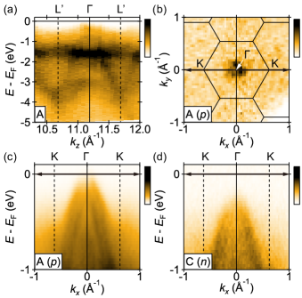
Although SX-ARPES measurements were successful, ARPES measurements using VUV light, which is typically used in studies of Weyl semimetals, could not detect any dispersion around the Fermi level (Note 6 in the Supplemental Material [30]). The difference in SX- and VUV-ARPES results is caused by the rough cleaved surface of the spinel . We will argue this point later.
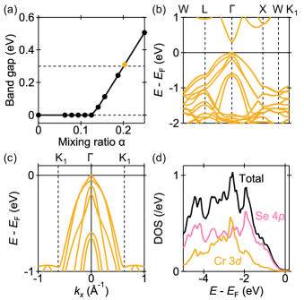
We further analyzed the electronic structure of by DFT calculations with the HSE06 hybrid functional. In the HSE06 functional, represents the mixing ratio of the Hartree-Fock exact exchange into the Perdew-Burke-Ernzerhof (PBE) exchange-correlation functional [44] of the GGA type; corresponds to the original PBE functional, and is the standard HSE06 value. The PBE functional gives a semimetallic band structure with magnetic Weyl points near the Fermi level [23]. However, the standard local density approximation and GGA exchange-correlation functionals often underestimate the band gaps of semiconductors, even occasionally yielding incorrect gap closing. That is why the exact exchange is included in hybrid functionals to mitigate this problem [11]. Recent first-principles examinations [45, 46] have suggested that the optimum value of for accurate band gap prediction may be smaller in narrow-gap semiconductors. To see the robustness of the gap opening, we, therefore, calculated the electronic structure with various between 0 and 0.25. Figure 3(a) shows the band gaps for different values. A nonzero mixing ratio yields a gapped electronic structure for and the band gap increases with increasing [Fig. 3(a)].
Here we show the calculated band structure with [orange point in Fig. 3(a)], where the band gap (0.31 eV) was approximately the same as the experimental one at low temperatures [19]; as discussed above, the band gap size depends on the temperature but is independent of the carrier type. Note 7 in the Supplemental Material [30] represents the calculation result with . Figure 3(c) shows the band dispersion along the direction, which agrees well with the experimental results [Figs. 2(c) and (d)]. While the magnetic moments of the calculated electronic structure are aligned along the vertical direction in Fig. 1(b), the symmetry lowering due to the ferromagnetism is negligible (Note 8 in the Supplemental Material [30]). The calculated density of states [Fig. 3(d)] shows the contribution of Cr and Se orbitals to the valence band, and the contribution of Cr orbitals is consistent with our resonant PES measurements (Note 9 in the Supplemental Material [30]). Our DFT calculations exhibit that the hybrid functional with the appropriate mixing ratio reproduces both the band gap determined by infrared spectra and the band dispersion obtained by SX-ARPES.
As was noted earlier, the roughness of the cleaved surface of the spinel affects photoemission spectra particularly in VUV-ARPES. The followinig argument about the rough surface illustrates the benefit of using SX-ARPES to observe the band dispersion of a material that does not have a good cleaving plane.
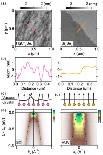
The AFM images in Figs. 4(a) and 4(b) compare the cleaved surfaces of and , which is a quintuple-layered material hosting topological surface states [47, 48]. The cleaved surface of is indeed rough, while exhibits large flat terraces with occasional steps, reflecting the layered structure. Compared to the flat surface assumed in typical ARPES measurements, the uneven surface of will create an unusual situation when photoelectrons escape from the crystal to the vacuum. Although the electronic structure of the rough surface region can be greatly different from that of the bulk, the photoemission from such an incoherent electronic structure is expected to be very weak because, roughly speaking, the photoemission probability is determined by the matrix element of the ground state and the plane wave. Therefore we think our ARPES spectra come from the photoemission in the deeper region [Fig. S10 in the Supplemental Material [30]], in which the electronic structure is sufficiently related to the bulk. The clear dispersion [Fig. 2(a)] and the coincidence with the calculated bulk band dispersion [Fig. 3(c)] support our argument.
In the three-step model [1], when a photoelectron escape from the crystal, the out-of-plane component of the photoelectron wavevector is modified while the in-plane component is unchanged [Fig. S11 in the Supplemental Material [30]]. While standard ARPES studies discuss the refraction of the photoelectron using a flat plane as shown in Fig. 4(d), such an analysis cannot be applied straightforwardly to with a rough cleaved surface. We simulated the photoemission from a rough surface as a sum of photoemission spectra from randomly-oriented flat surfaces [Fig. 4(c) and Ref. [49]] using the hole band dispersion in Fig. 2(c). The simulated spectra in the SX and VUV regions are shown in Fig. 4(e) for photon energies that are approximately the same as in the experiments. A slightly broadened parabolic dispersion is retained in the SX region. However, the simulated spectra in the VUV region are too broad to see a dispersion curve. The constant energy maps also exhibit the similar behavior [Fig. S12 in the Supplemental Material [30]]. This difference arises because the wavevector of a photoelectron in the VUV region is shorter than that in the SX region and, therefore, more strongly refracted [Fig. S13 in the Supplemental Material [30]]. A clear advantage of SX-ARPES over VUV-ARPES is thus that SX-ARPES can be used to study materials that are not easy to cleave and therefore suffer from increased surface roughness. We note that the bulk sensitivity of SX-ARPES [50] and a micro-focused beam of a dedicated SX-ARPES beamline [36] can also contribute to the clear dispersion observed in the SX-ARPES experiments.
In conclusion, we show for the first time the ARPES result of the ferromagnetic spinel , which is direct evidence for the semiconducting electronic structure of this material. SX-ARPES was used to visualize the valence band dispersion of . We only observed hole bands while electron bands were absent below the Fermi level. These ARPES results are consistent with the existence of a band gap determined by infrared transmittance spectra. DFT calculations with the HSE06 hybrid functional reproduced the gapped band dispersion. We adjusted the mixing ratio of the HSE06 functional so that the calculations gave the experimentally observed band gap, and obtained dispersion curves that agreed well with our ARPES result. Our study draws attention to choosing appropriate functionals in DFT calculations and the advantage of SX-ARPES in investigating the electronic structure of solid crystals.
Acknowledgements.
We thank Y. Ishida for supporting the analysis of ARPES data [51], and P. Zhang, S. Sakuragi, and R. Noguchi for supporting our SX-ARPES experiments. A.V.T. thanks the Brain Pool (BP) Program funded by the Ministry of Science and ICT (MSIT) (No. 2021H1D3A2A01096552). V.A.G. and O.E.T. acknowledge support from the Russian Science Foundation (Grant No. 22-12-20024) and the government of the Novosibirsk region (p-9). K.K. acknowledges support from the Murata Science Foundation and the Futaba research grant program. This work is also supported by Grant-in-Aid for JSPS Fellows (Grant No. JP21J20657), Grant-in-Aid for Early-Career Scientists (Grant No. JP21K13858), Grant-in-Aid for Scientific Research on Innovative Areas (Grant No. JP22H04483), Grant-in-Aid for Scientific Research (B) (Grant No. JP22H01943) Grant-in-Aid for Scientific Research (A) (Grants No. JP21H04652 and No. JP21H04439), Japan Science and Technology Agency (JST) (Grant No. JPMJMI21G2), JST, PRESTO (Grant No. JPMJPR20LA), program of Ministry of Education and Science of the Russian Federation (“Spin” No. 122021000036-3), Quantum Leap Flagship Program from Ministry of Education, Culture, Sports, Science and Technology (MEXT Q-LEAP) (Grant No. JPMXS0118068681), and Photon and Quantum Basic Research Coordinated Development Program from MEXT. Transmission spectroscopy and Laue back-reflection measurements were performed using the facilities of the Materials Design and Characterization Laboratory in the Institute for Solid State Physics (ISSP), the University of Tokyo. Some of the calculations were performed at the Supercomputer Center in ISSP, the University of Tokyo. The synchrotron radiation experiments were performed with the approval of UVSOR (Proposals No. 20-757 and No. 20-842) and JASRI (Proposals No. 2019B1092 and No. 2020A0606).References
- Sobota et al. [2021] J. A. Sobota, Y. He, and Z.-X. Shen, Rev. Mod. Phys. 93, 025006 (2021).
- Xu et al. [2015] S.-Y. Xu, I. Belopolski, N. Alidoust, M. Neupane, G. Bian, C. Zhang, R. Sankar, G. Chang, Z. Yuan, C.-C. Lee, S.-M. Huang, H. Zheng, J. Ma, D. S. Sanchez, B. Wang, A. Bansil, F. Chou, P. P. Shibayev, H. Lin, S. Jia, and M. Z. Hasan, Science 349, 613 (2015).
- Lv et al. [2015] B. Q. Lv, N. Xu, H. M. Weng, J. Z. Ma, P. Richard, X. C. Huang, L. X. Zhao, G. F. Chen, C. E. Matt, F. Bisti, V. N. Strocov, J. Mesot, Z. Fang, X. Dai, T. Qian, M. Shi, and H. Ding, Nature Physics 11, 724 (2015).
- Yang et al. [2015] L. X. Yang, Z. K. Liu, Y. Sun, H. Peng, H. F. Yang, T. Zhang, B. Zhou, Y. Zhang, Y. F. Guo, M. Rahn, D. Prabhakaran, Z. Hussain, S.-K. Mo, C. Felser, B. Yan, and Y. L. Chen, Nature Physics 11, 728 (2015).
- Yao et al. [2019] M.-Y. Yao, N. Xu, Q. S. Wu, G. Autès, N. Kumar, V. N. Strocov, N. C. Plumb, M. Radovic, O. V. Yazyev, C. Felser, J. Mesot, and M. Shi, Phys. Rev. Lett. 122, 176402 (2019).
- Kuroda et al. [2017] K. Kuroda, T. Tomita, M.-T. Suzuki, C. Bareille, A. A. Nugroho, P. Goswami, M. Ochi, M. Ikhlas, M. Nakayama, S. Akebi, R. Noguchi, R. Ishii, N. Inami, K. Ono, H. Kumigashira, A. Varykhalov, T. Muro, T. Koretsune, R. Arita, S. Shin, T. Kondo, and S. Nakatsuji, Nature Materials 16, 1090 (2017).
- Liu et al. [2019] D. F. Liu, A. J. Liang, E. K. Liu, Q. N. Xu, Y. W. Li, C. Chen, D. Pei, W. J. Shi, S. K. Mo, P. Dudin, T. Kim, C. Cacho, G. Li, Y. Sun, L. X. Yang, Z. K. Liu, S. S. P. Parkin, C. Felser, and Y. L. Chen, Science 365, 1282 (2019).
- Hohenberg and Kohn [1964] P. Hohenberg and W. Kohn, Phys. Rev. 136, B864 (1964).
- Kohn and Sham [1965] W. Kohn and L. J. Sham, Phys. Rev. 140, A1133 (1965).
- Aulbur et al. [2000] W. G. Aulbur, L. Jönsson, and J. W. Wilkins, Quasiparticle Calculations in Solids, edited by H. Ehrenreich and F. Spaepen, Solid State Physics, Vol. 54 (Academic Press, 2000) pp. 1–218.
- Marsman et al. [2008] M. Marsman, J. Paier, A. Stroppa, and G. Kresse, Journal of Physics: Condensed Matter 20, 064201 (2008).
- Baltzer et al. [1965] P. K. Baltzer, H. W. Lehmann, and M. Robbins, Phys. Rev. Lett. 15, 493 (1965).
- Baltzer et al. [1966] P. K. Baltzer, P. J. Wojtowicz, M. Robbins, and E. Lopatin, Phys. Rev. 151, 367 (1966).
- Minematsu et al. [1971] K. Minematsu, K. Miyatani, and T. Takahashi, Journal of the Physical Society of Japan 31, 123 (1971).
- Selmi et al. [1986] A. Selmi, M. Heritier, and P. Gibart, Progress in Crystal Growth and Characterization 13, 121 (1986).
- Bebenin et al. [2015] N. Bebenin, R. Zainullina, and Y. P. Sukhorukov, Journal of Magnetism and Magnetic Materials 387, 127 (2015).
- Goldstein et al. [1978] L. Goldstein, P. Gibart, and A. Selmi, Journal of Applied Physics 49, 1474 (1978).
- Lehmann and Emmenegger [1969] H. Lehmann and F. Emmenegger, Solid State Communications 7, 965 (1969).
- Arai et al. [1973] T. Arai, M. Wakaki, S. Onari, K. Kudo, T. Satoh, and T. Tsushima, Journal of the Physical Society of Japan 34, 68 (1973).
- Auslender et al. [1989] M. Auslender, E. V. Barsukova, N. Bebenin, B. Gizhevskii, N. Loshkareva, Y. P. Sukhorukov, and N. Chebotaev, Sov. Phys. JETP 68, 139 (1989).
- Auslender and Bebenin [1989] M. Auslender and N. Bebenin, Solid State Communications 69, 761 (1989).
- Kostylev et al. [1990] V. A. Kostylev, B. A. Gizhevskii, A. A. Samokhvalov, M. I. Auslender, and N. G. Bebenin, physica status solidi (b) 158, 307 (1990).
- Xu et al. [2011] G. Xu, H. Weng, Z. Wang, X. Dai, and Z. Fang, Phys. Rev. Lett. 107, 186806 (2011).
- Wan et al. [2011] X. Wan, A. M. Turner, A. Vishwanath, and S. Y. Savrasov, Phys. Rev. B 83, 205101 (2011).
- Guan et al. [2015] T. Guan, C. Lin, C. Yang, Y. Shi, C. Ren, Y. Li, H. Weng, X. Dai, Z. Fang, S. Yan, and P. Xiong, Phys. Rev. Lett. 115, 087002 (2015).
- Yang et al. [2019] S. Yang, Z. Li, C. Lin, C. Yi, Y. Shi, D. Culcer, and Y. Li, Phys. Rev. Lett. 123, 096601 (2019).
- Li and Levchenko [2020] S. Li and A. Levchenko, Phys. Rev. Lett. 124, 156802 (2020).
- Guo and Liu [2012] S.-D. Guo and B.-G. Liu, Journal of Physics: Condensed Matter 24, 045502 (2012).
- Tran and Blaha [2009] F. Tran and P. Blaha, Phys. Rev. Lett. 102, 226401 (2009).
- [30] See Supplemental Material at [URL] for additional experimental and simulation data, which includes Refs. [49] and [50].
- van Setten et al. [2018] M. van Setten, M. Giantomassi, E. Bousquet, M. Verstraete, D. Hamann, X. Gonze, and G.-M. Rignanese, Computer Physics Communications 226, 39 (2018).
- Maeda et al. [2018] M. Maeda, K. Yamamoto, T. Mizokawa, N. L. Saini, M. Arita, H. Namatame, M. Taniguchi, G. Tan, L. D. Zhao, and M. G. Kanatzidis, Phys. Rev. B 97, 121110 (2018).
- Selmi et al. [1980] A. Selmi, P. Gibart, and L. Goldstein, Journal of Magnetism and Magnetic Materials 15-18, 1285 (1980).
- Solin and Naumov [2000] N. I. Solin and S. V. Naumov, Journal of Experimental and Theoretical Physics Letters 72, 612 (2000).
- Solin et al. [2008] N. I. Solin, V. V. Ustinov, and S. V. Naumov, Physics of the Solid State 50, 901 (2008).
- Muro et al. [2021] T. Muro, Y. Senba, H. Ohashi, T. Ohkochi, T. Matsushita, T. Kinoshita, and S. Shin, Journal of Synchrotron Radiation 28, 1631 (2021).
- Giannozzi et al. [2017] P. Giannozzi, O. Andreussi, T. Brumme, O. Bunau, M. B. Nardelli, M. Calandra, R. Car, C. Cavazzoni, D. Ceresoli, M. Cococcioni, N. Colonna, I. Carnimeo, A. D. Corso, S. de Gironcoli, P. Delugas, R. A. DiStasio, A. Ferretti, A. Floris, G. Fratesi, G. Fugallo, R. Gebauer, U. Gerstmann, F. Giustino, T. Gorni, J. Jia, M. Kawamura, H.-Y. Ko, A. Kokalj, E. Küçükbenli, M. Lazzeri, M. Marsili, N. Marzari, F. Mauri, N. L. Nguyen, H.-V. Nguyen, A. O. de-la Roza, L. Paulatto, S. Poncé, D. Rocca, R. Sabatini, B. Santra, M. Schlipf, A. P. Seitsonen, A. Smogunov, I. Timrov, T. Thonhauser, P. Umari, N. Vast, X. Wu, and S. Baroni, Journal of Physics: Condensed Matter 29, 465901 (2017).
- Pizzi et al. [2020] G. Pizzi, V. Vitale, R. Arita, S. Blügel, F. Freimuth, G. Géranton, M. Gibertini, D. Gresch, C. Johnson, T. Koretsune, J. Ibañez-Azpiroz, H. Lee, J.-M. Lihm, D. Marchand, A. Marrazzo, Y. Mokrousov, J. I. Mustafa, Y. Nohara, Y. Nomura, L. Paulatto, S. Poncé, T. Ponweiser, J. Qiao, F. Thöle, S. S. Tsirkin, M. Wierzbowska, N. Marzari, D. Vanderbilt, I. Souza, A. A. Mostofi, and J. R. Yates, Journal of Physics: Condensed Matter 32, 165902 (2020).
- Heyd et al. [2003] J. Heyd, G. E. Scuseria, and M. Ernzerhof, The Journal of Chemical Physics 118, 8207 (2003).
- Heyd et al. [2006] J. Heyd, G. E. Scuseria, and M. Ernzerhof, The Journal of Chemical Physics 124, 219906 (2006).
- Marzari and Vanderbilt [1997] N. Marzari and D. Vanderbilt, Phys. Rev. B 56, 12847 (1997).
- Souza et al. [2001] I. Souza, N. Marzari, and D. Vanderbilt, Phys. Rev. B 65, 035109 (2001).
- Sun et al. [2019] J. P. Sun, Y. Y. Jiao, C. J. Yi, S. E. Dissanayake, M. Matsuda, Y. Uwatoko, Y. G. Shi, Y. Q. Li, Z. Fang, and J.-G. Cheng, Phys. Rev. Lett. 123, 047201 (2019).
- Perdew et al. [1996] J. P. Perdew, M. Ernzerhof, and K. Burke, The Journal of Chemical Physics 105, 9982 (1996).
- Alkauskas et al. [2011] A. Alkauskas, P. Broqvist, and A. Pasquarello, physica status solidi (b) 248, 775 (2011).
- Skone et al. [2014] J. H. Skone, M. Govoni, and G. Galli, Phys. Rev. B 89, 195112 (2014).
- Zhang et al. [2009] H. Zhang, C.-X. Liu, X.-L. Qi, X. Dai, Z. Fang, and S.-C. Zhang, Nature Physics 5, 438 (2009).
- Xia et al. [2009] Y. Xia, D. Qian, D. Hsieh, L. Wray, A. Pal, H. Lin, A. Bansil, D. Grauer, Y. S. Hor, R. J. Cava, and M. Z. Hasan, Nature Physics 5, 398 (2009).
- [49] The source code and the input files for the simulation are available from https://github.com/Hiroaki-Tanaka-0606/Photoelectron_refraction.
- Strocov et al. [2019] V. Strocov, L. Lev, M. Kobayashi, C. Cancellieri, M.-A. Husanu, A. Chikina, N. Schröter, X. Wang, J. Krieger, and Z. Salman, Journal of Electron Spectroscopy and Related Phenomena 236, 1 (2019).
- Ishida and Shin [2018] Y. Ishida and S. Shin, Review of Scientific Instruments 89, 043903 (2018).