Mixed-dimensional moiré systems of graphitic thin films with a twisted interface
Moiré patterns formed by stacking atomically-thin van der Waals crystals with a relative twist angle can give rise to dramatic new physical properties Balents2020 ; Andrei2020 . The study of moiré materials has so far been limited to structures comprising no more than a few vdW sheets, since a moiré pattern localized to a single two-dimensional interface is generally assumed to be incapable of appreciably modifying the properties of a bulk three-dimensional crystal. Layered semimetals such as graphite offer a unique platform to challenge this paradigm, owing to distinctive properties arising from their nearly-compensated electron and hole bulk doping. Here, we perform transport measurements of dual-gated devices constructed by slightly rotating a monolayer graphene sheet atop a thin bulk graphite crystal. We find that the moiré potential transforms the electronic properties of the entire bulk graphitic thin film. At zero and small magnetic fields, transport is mediated by a combination of gate-tunable moiré and graphite surface states, as well as coexisting semimetallic bulk states that do not respond to gating. At high field, the moiré potential hybridizes with the graphitic bulk states owing to the unique properties of the two lowest Landau bands of graphite. These Landau bands facilitate the formation of a single quasi–two-dimensional hybrid structure in which the moiré and bulk graphite states are inextricably mixed. Our results establish twisted graphene-graphite as the first in a new class of mixed-dimensional moiré materials.
Twisting two sheets of monolayer graphene by a small angle results in the formation of a long-wavelength moiré potential that substantially alters the low-energy bands Bistritzer2011 ; Morell2010 . The moiré bands become extremely flat and isolated near the “magic angle” of approximately , generating an array of strongly correlated states including magnetism and superconductivity Cao2018a ; Cao2018b ; Lu2019 ; Yankowitz2019 ; Balents2020 ; Andrei2020 . Moiré flat bands also form upon incorporating additional graphene sheets into the structure, recently observed in the magic-angle trilayer/tetralayer/pentalayer family Park2021 ; Hao2021 ; Park2022 ; Burg2022 ; Zhang2022 as well as in twisted monolayer-bilayer Chen2021 ; Polshyn2020 ; Shi2021 ; He2021tmbg and bilayer-bilayer graphene Shen2020 ; Liu2020 ; Cao2020 ; Burg2019 ; He2021tdbg . So far, the study of twisted graphene structures has mostly been limited to those assembled from monolayer and bilayer graphene building blocks, since thicker Bernal-stacked constituents contribute additional bands at low energy. Band structure modeling indicates that moiré bands are likely to persist to arbitrarily thick Bernal graphite structures, but remain localized at the twisted interface and coexist with conventional bulk graphite bands Cea2019 . Moiré surface states have been observed previously in scanning tunneling microscopy experiments performed on highly oriented pyrolitic graphite with a rotationally faulted surface sheet Li2010 . However, it is currently not know whether and how these moiré surface states impact the electronic properties of the entire bulk graphitic thin film.
Here, we investigate the transport properties of graphitic structures with a moiré interface created by a single rotational fault within the crystal. We primarily focus on the case where the moiré potential is localized to one surface of the structure, achieved by rotating a flake of monolayer graphene by a small twist angle atop a Bernal graphite thin film. We also compare to the case where the moiré interface is buried at the center of the graphitic structure. We show that a single two-dimensional moiré interface can strongly modify the properties of the entire graphitic thin film, owing to a number of unique properties arising from its semimetallic nature. At zero and small magnetic fields, we find that the electronic transport can be well approximated by parallel contributions of gate-induced surface accumulation layers and intrinsic bulk states. In the case where the twisted interface is located at an outer surface of the sample, the transport properties are dominated by moiré surface bands and differ considerably from Bernal graphite. At high magnetic fields, the moiré and bulk states become inextricably mixed by a standing wave formed along the -axis of graphite. The entire graphitic thin film becomes quasi–two-dimensional in this regime, forming a novel mixed-dimensional moiré system.
Comparison of transport in Bernal and moiré graphite
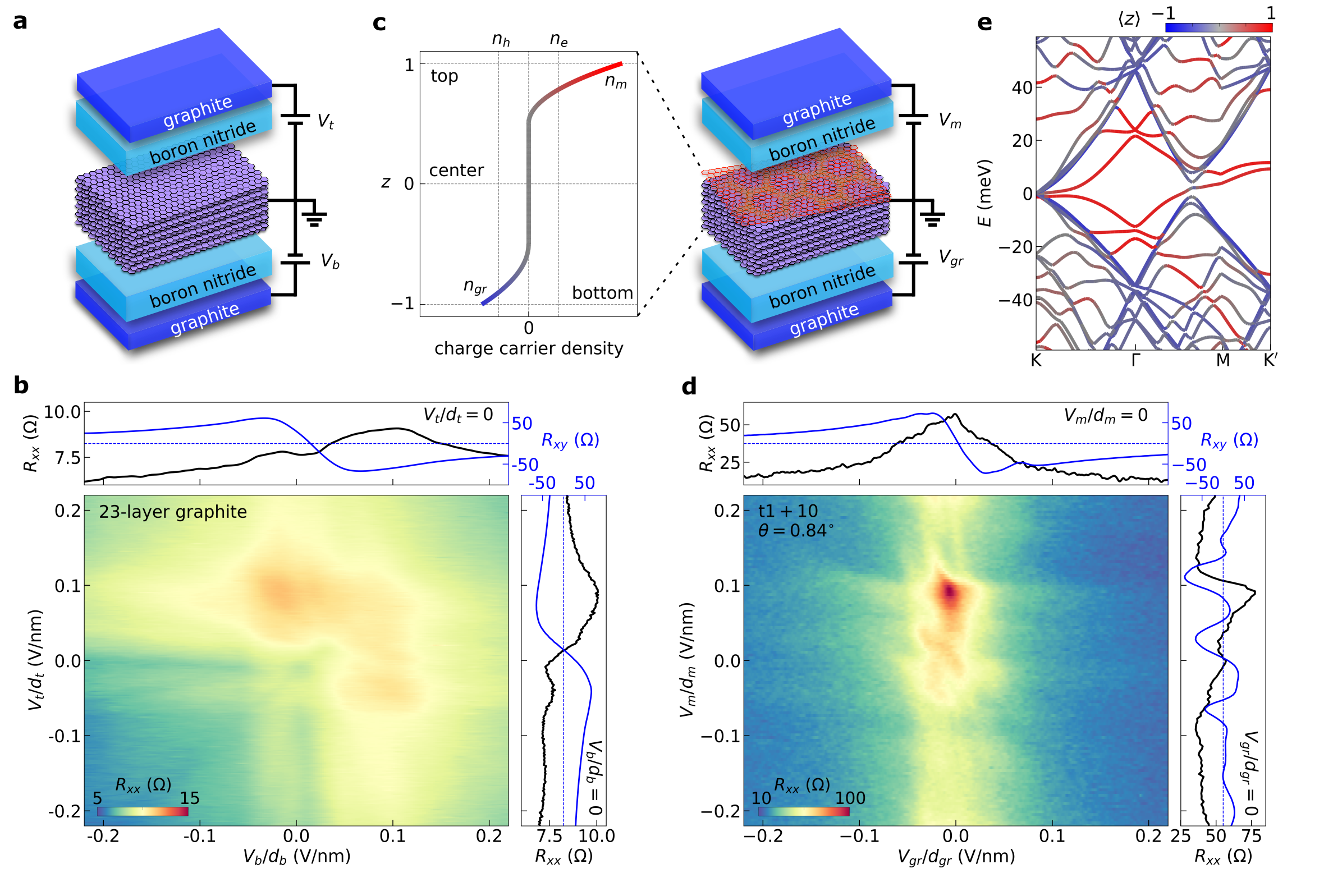
We focus our study primarily on twisted graphene-graphite (i.e., t1+, where indicates monolayer graphene and corresponds to the number of graphene sheets in the bulk thin film). We measure devices with graphite thickness varying from to layers, and with twist angles between and . These structures are encapsulated between flakes of boron nitride (BN), and capped by additional graphite flakes acting as top and bottom gates (see Methods for additional details). All transport measurements are performed at a base temperature of 1.7 K, unless otherwise noted. We first compare the transport properties of Bernal graphite with a representative twisted graphene-graphite device. Figure 1 shows this for the case of a 23-layer Bernal graphite device and a t1+10 device with . A schematic of the Bernal graphite device is shown in Fig. 1a, with top and bottom gate voltages denoted as and , respectively.
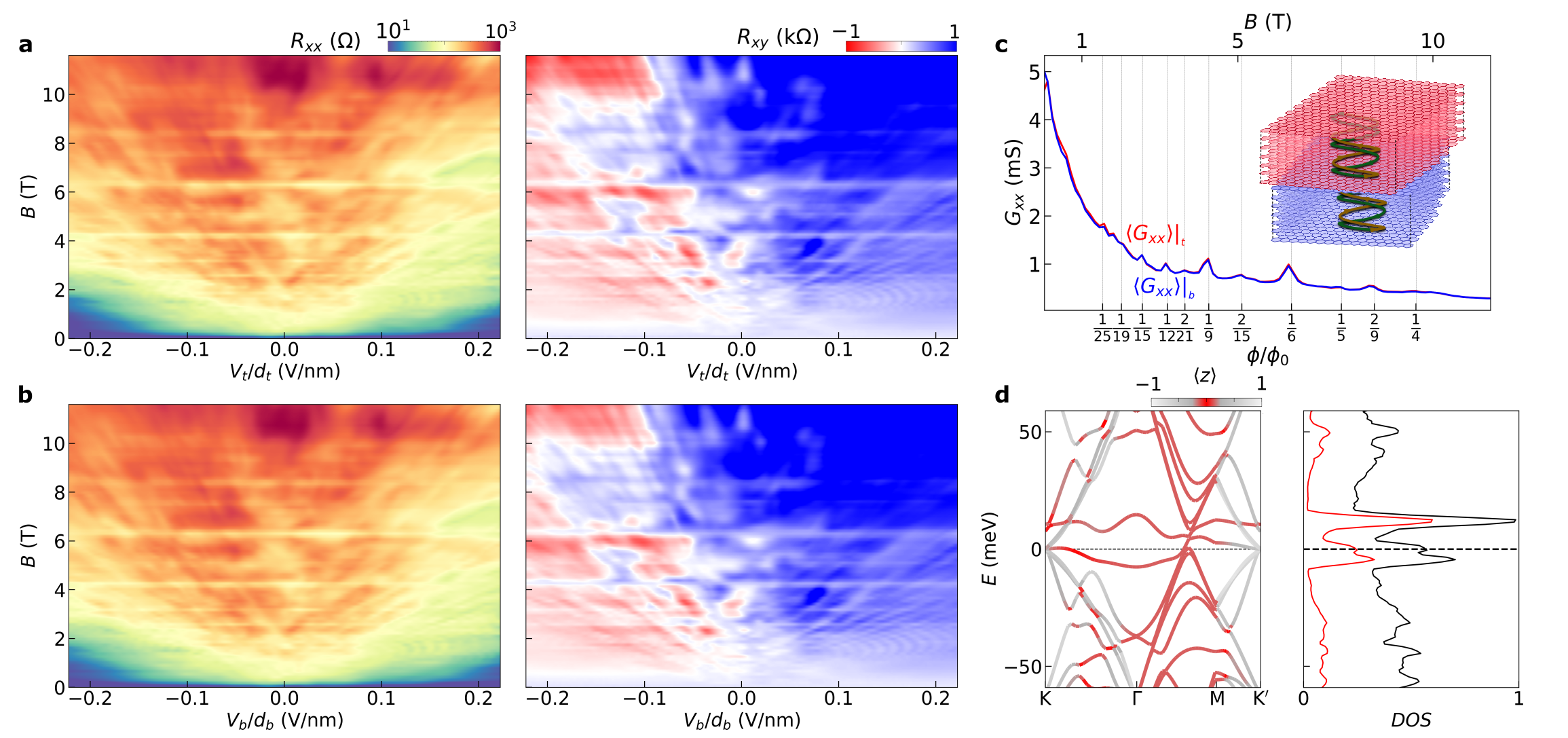
The color map in Fig. 1b shows the longitudinal resistance, , of the device at zero magnetic field as a function of the voltage on both gates (each gate voltage is normalized by the corresponding BN dielectric thickness). The resistance changes by only a few ohms with gating, consistent with the expectation that the gates are only able to dope the outer few layers of the nearest graphite surface due to screening in the bulk. Consequentially, the primary resistance features we observe evolve either vertically or horizontally in the map. Although the resistance map exhibits fine structure that we do not fully understand, we find that transport is very similar upon sweeping each gate with the other held fixed. This behavior is anticipated from the mirror symmetry of Bernal graphite, with small differences likely resulting from a variation in mobility between the two surfaces. This can also be seen by comparing the black traces in the panels above and to the right of the resistance map, which show as each gate is swept with the other held at ground. We further see corroborating behavior in the Hall resistance, , measured in a small magnetic field of T. In particular, exhibits a sign change around zero bias in each gate sweep, signifying a corresponding sign change in the charge of the free carriers residing in the surface accumulation layer.
In contrast to our observations in Bernal graphite, transport in our t1+10 sample differs considerably depending on which gate is swept, as the mirror symmetry of the structure is broken by the rotated graphene sheet at the surface. Here, we denote the voltage on the gate facing the moiré (Bernal graphite) surface as () (see Fig. 1c). We see a much larger change in the resistance with gating in this device (Fig. 1d), with the highest resistance confined to a small region around . Transport is reminiscent of Bernal graphite when sweeping (see and traces in the top panel), but exhibits fundamentally new behavior when sweeping (right panel). In particular, repeated sign changes indicate multiple instances in which the free carriers on the twisted surface switch between electron- and hole-like. This behavior arises from the moiré reconstruction of the graphite band structure, marking the formation of a series of surface-localized moiré bands. These can be seen in calculations of the band structure of this material (Fig. 1e, see Methods for details). The bands are color-coded based upon their expectation value along the graphite -axis, denoted as , where a value of 1 (-1) corresponds to the moiré (Bernal graphite) surface. We find moiré bands localized on the outer graphene layers at the rotated interface (red colored bands), consistent with previous calculations performed for infinitely thick graphite slabs Cea2019 .
Despite the differences between the Bernal and moiré graphite devices, the gate-dependent transport of both are dominated by their surfaces. Figure 1c illustrates this schematically for the twisted graphene-graphite device, where a charge carrier density of () can be induced on the moiré (Bernal) surface by tuning (). The graphite bulk remains a compensated semimetal, with roughly equal electron- and hole-doping ( and ) that does not change with gating.
Low-field magnetotransport properties of moiré graphite
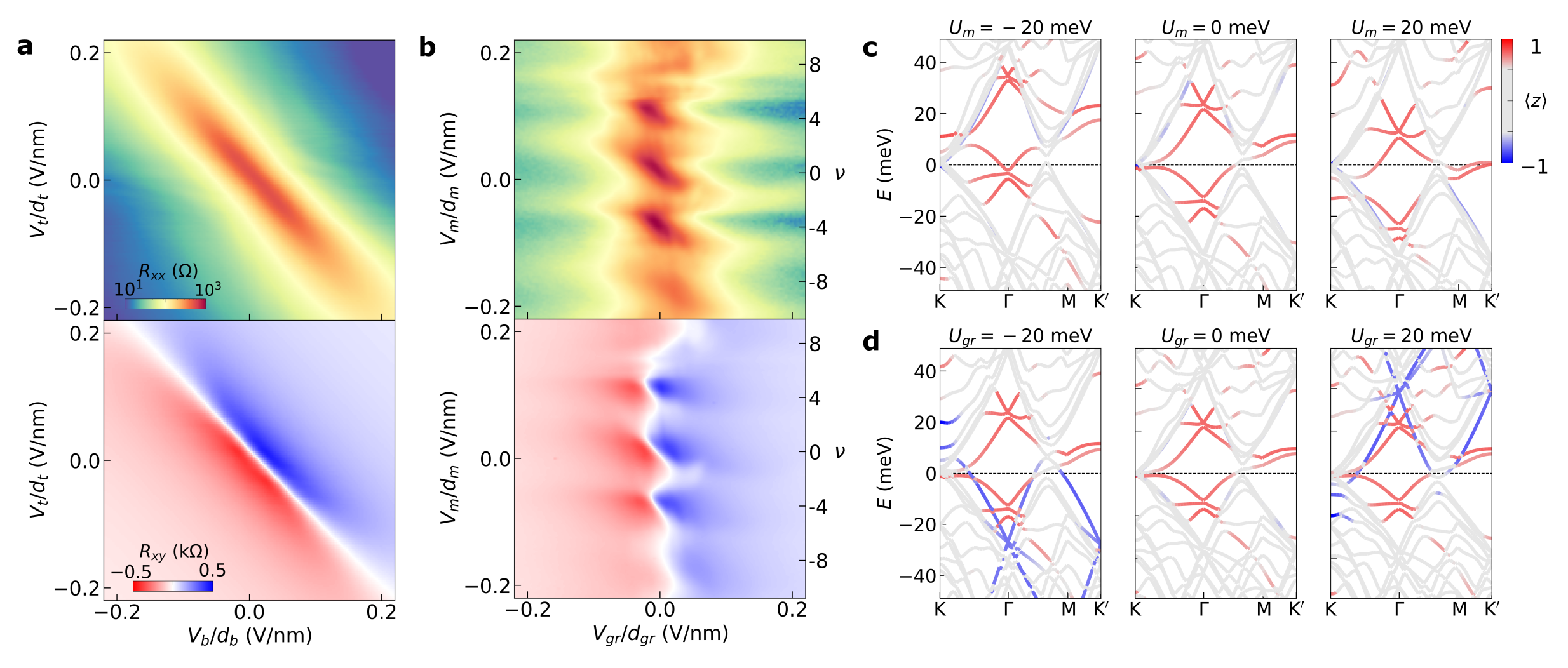
The contrast between Bernal and moiré graphite becomes more obvious upon applying a small magnetic field along the -axis. Figure 2a shows a dual-gate resistance map for the 23-layer Bernal graphite sample acquired at a magnetic field of T. The resistance is largest when the voltage on both gates is approximately zero, consistent with prior reports of a large magnetoresistance (MR) in bulk graphite crystals Soule1958 . Upon gating, we additionally find a large MR everywhere along the condition of overall charge neutrality, , as evidenced by the diagonal resistance stripe in Fig. 2a. Measurements of the Hall resistance show a corresponding sign change across the line of overall neutrality.
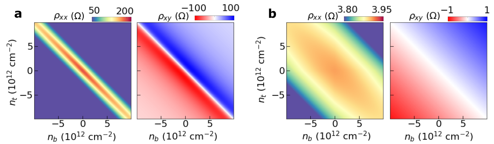
These observations can be captured by a four-carrier Drude transport model, in which we assume that transport is mediated by coexisting electron and hole bulk carriers that do not respond to gating, along with gate-modulated surface accumulation layers controlled independently by the top and bottom gates (see Methods for full details). Extended Data Figure 1a shows the result of this calculation, taking the known mobility and bulk charge doping of graphite Soule1958 ; McClure1958 . The excellent agreement between our measurements and this calculation indicates that transport is primarily determined by the total free charge density in the material, even when the gate-induced charge is mostly localized at the outer surfaces. This behavior arises as a consequence of the low intrinsic bulk doping of graphite, as similar calculations performed with orders-of-magnitude larger bulk doping show virtually no gate tunability (Extended Data Fig. 1b).
Corresponding measurements of the moiré sample reveal a more complex dependence of transport on gating (Fig. 2b and Extended Data Fig. 2). Rather than a single resistance stripe, exhibits a maximum that evolves with a peculiar zig-zag trajectory upon gating. The contour of tracks closely with the maximum. Notably, the periodic resets we observe upon biasing correspond closely with integer multiples of the gate voltage required to completely fill the four-fold degenerate surface moiré minibands, denoted by the band filling factor, , on the right-hand axis (see Methods for definition of ).
This behavior can be qualitatively captured by a simple model building upon the magnetotransport properties of Bernal graphite. Transport in the moiré sample evolves similarly to that of Bernal graphite as the two gate voltages are tuned slightly away from zero, forming a small diagonal resistance stripe. However, as is raised further, the surface moiré minibands evolve through a Lifshitz transition corresponding to a sign change in the mass of the free carriers. When corresponds to full filling of the moiré band (, the surface free charge density returns to approximately zero, and the transport once again mimics the local behavior surrounding . The sign of the Hall effect similarly flips as the doping at the moiré surface switches between electron- and hole-like, corresponding to instances in which Fermi energy crosses a moiré band extrema or a Lifshitz transition. For sufficiently large values of , the doping of the Bernal graphite surface exceeds the maximum doping possible in the narrow moiré band, and the sign of the Hall effect can no longer flip upon further biasing .
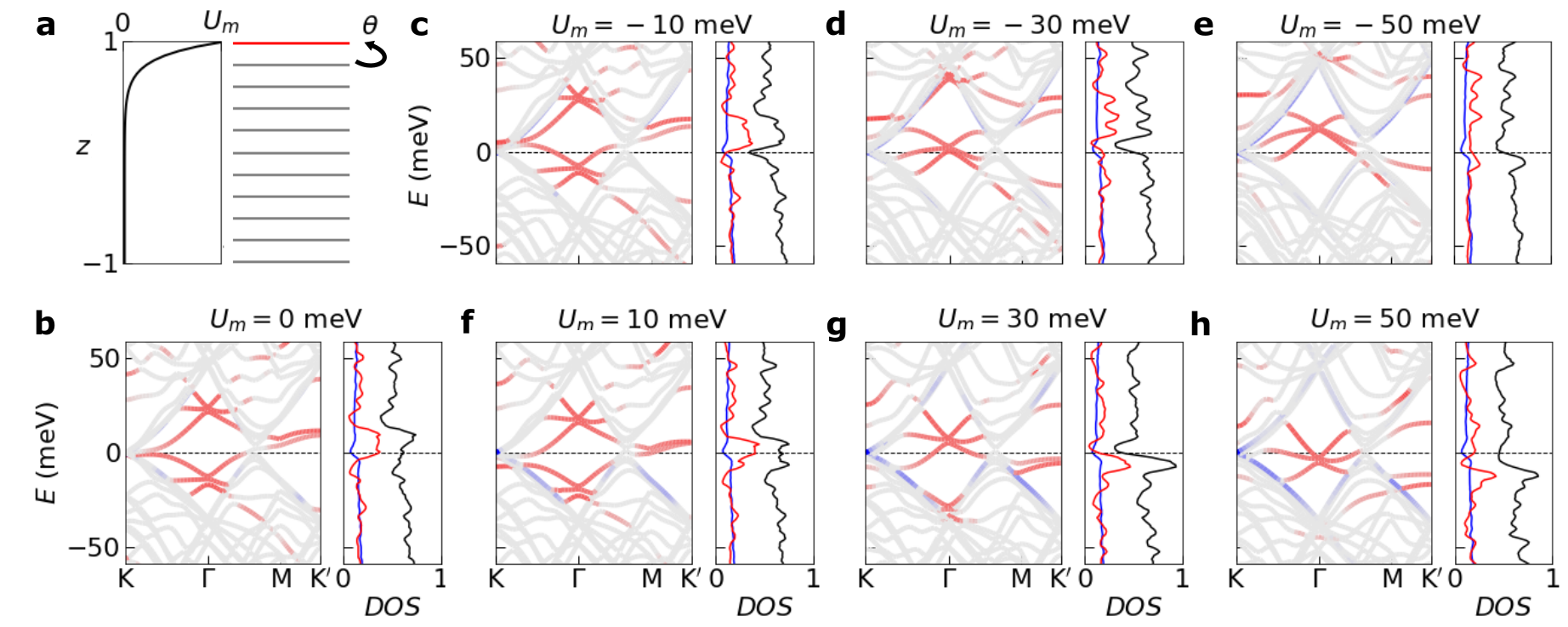
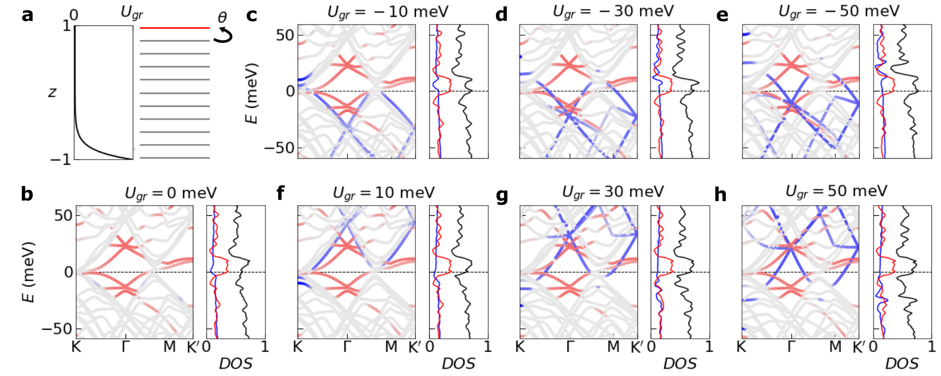
We verify this picture by calculating the band structure of twisted graphene-graphite with tunable gate-induced surface potentials (see Methods for full details). We adopt the Thomas-Fermi approximation to account for the screening of external electric fields by the graphite bulk Koshino2010 . Fig. 2c shows the evolution of the band structure for various values of the potential at the moiré surface, . The Fermi energy is denoted by the black dashed line, and is held fixed at zero energy. We find that gating primarily changes the energy of the moiré-like surface states, whereas the graphite-like states in the bulk remain at fixed energy. In contrast, the energy of the moiré-like bands remains fixed upon changing the potential at the Bernal graphite surface, , as shown in Fig. 2d. Instead, only graphite-like states change in energy, resulting in the filling of surface valence or conduction band states depending only on the sign of . These calculations support our interpretation of the zig-zag feature observed in transport, since the sign of the free carriers induced at the sample surfaces flips only once upon changing the sign of , but inverts repeatedly as the moiré surface bands are filled upon changing . Extended Data Figures 3 and 4 provide a more detailed analysis of these band structure calculations.
Hybridized moiré and bulk states at high field
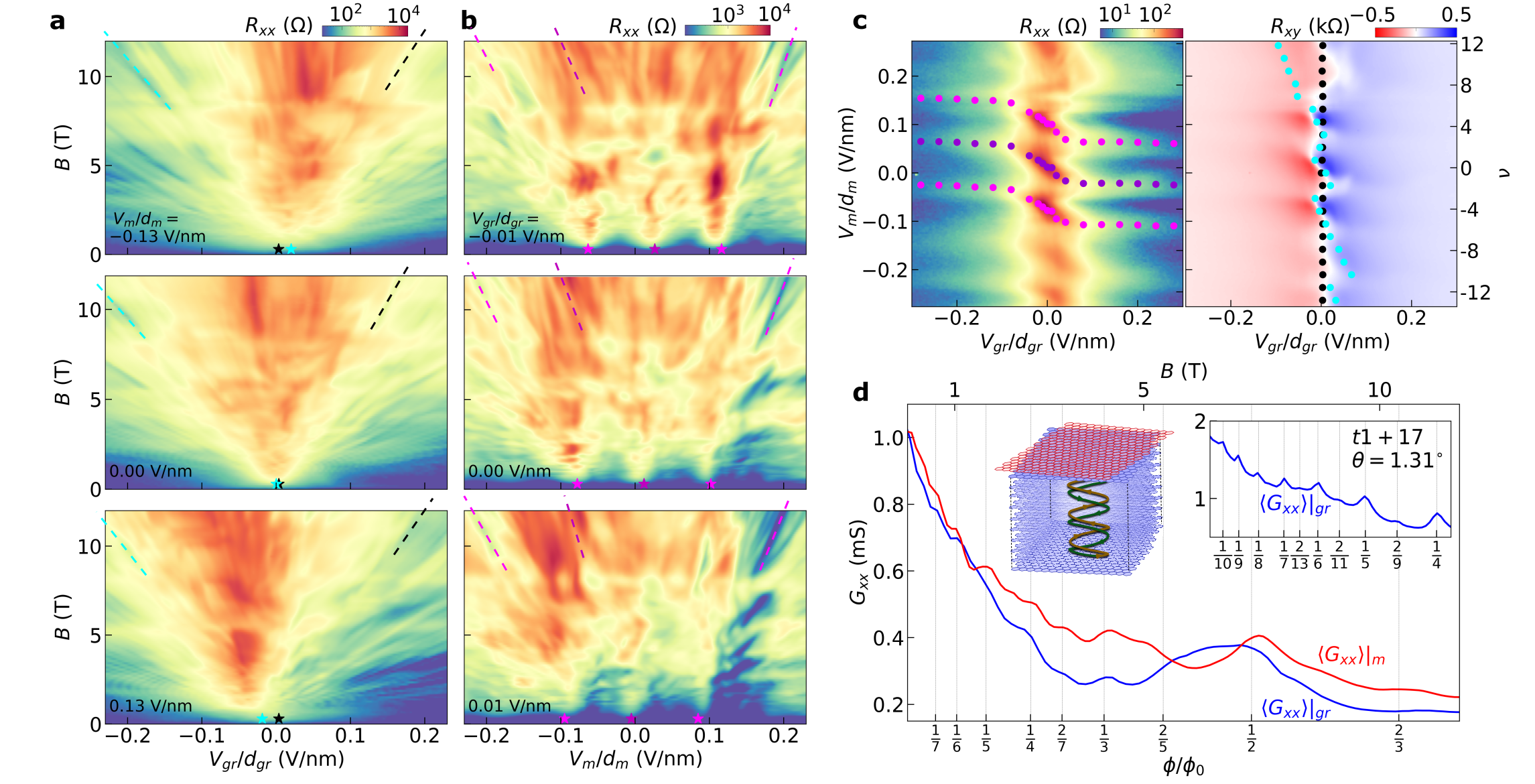
So far, we have found that the charge accumulation layers on the two surfaces do not directly hybridize with each other, and are thus controlled independently by the nearest gate. However, this behavior is known to break down in Bernal graphite at higher magnetic fields Yin2019 . In the ultra-quantum limit, only the two lowest (nearly-degenerate) Landau bands cross the Fermi energy, and the electron motion is primarily limited to the -axis McClure1968 ; Yin2019 . Electrons form a set of standing waves that penetrate across the entire bulk owing to the quasi-1D nature of these Landau bands. These states are thus controlled equally by the top and bottom gates. All other Landau bands are gapped within the bulk, and although they can be populated at the surfaces by gating, they form a screening layer and can only be controlled by the nearest gate. As a consequence, we find that Landau fans acquired by sweeping a single gate exhibit two distinct sets of quantum oscillations (QOs). One sequence projects to approximately zero gate voltage at , irrespective of the bias applied to the other gate. These QOs correspond to surface-localized states. The second sequence projects to a non-zero gate voltage determined by the bias applied to the opposite gate, in particular following the line of overall charge neutrality. These QOs correspond to states that are extended across the entire bulk (Extended Data Fig. 5).
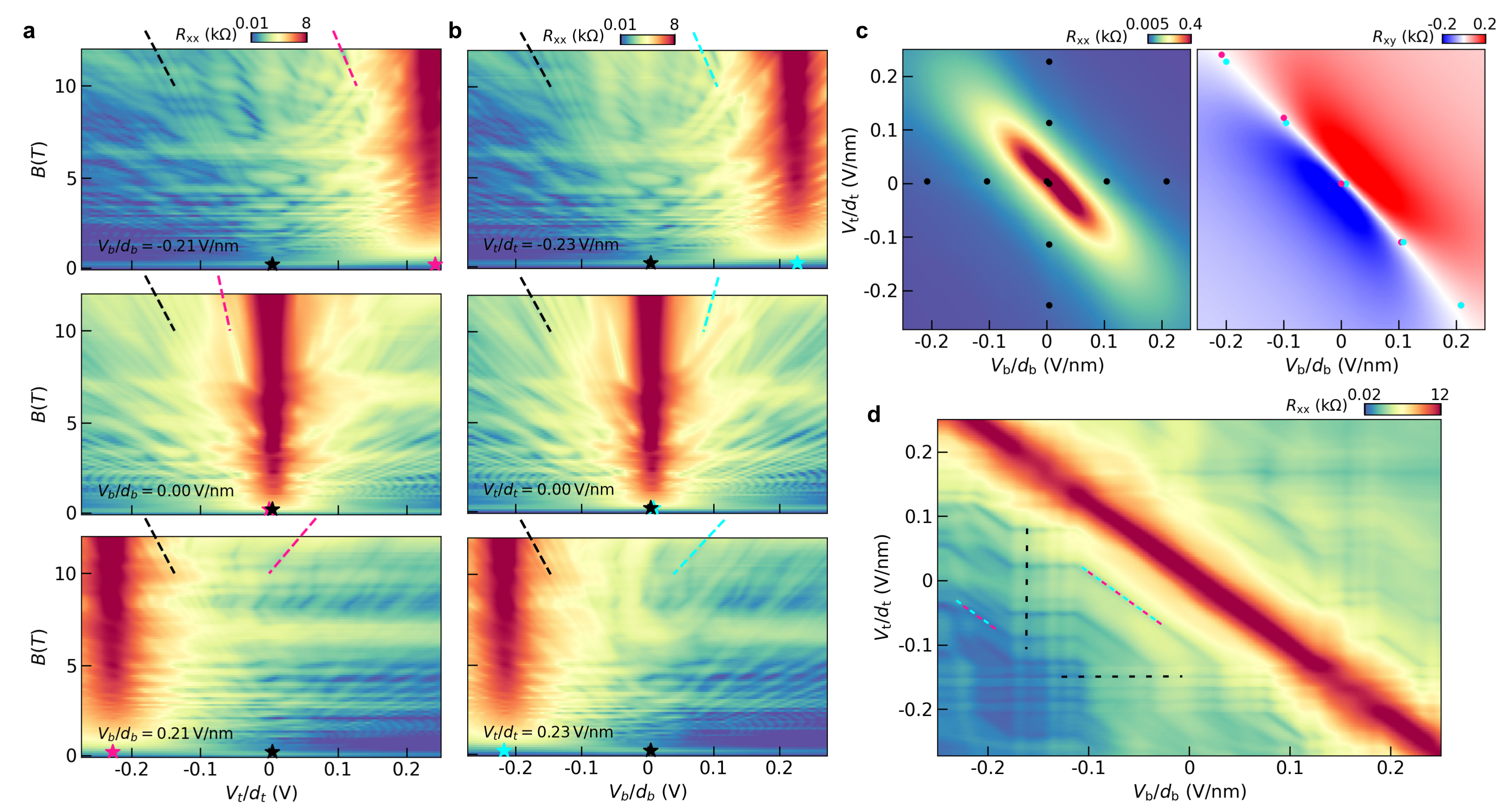
The moiré surface states in t1+ graphite form Hofstadter bands at high field Hofstadter1976 , which must smoothly evolve into the Bernal graphite Landau bands in the bulk. Despite this additional complexity, our magnetotransport measurements reveal that ungapped bulk states remain extended across the entire sample. We probe this effect by acquiring Landau fan diagrams while sweeping at various fixed values of (Fig. 3a). Similar to our observations in Bernal graphite, we see two distinct sequences of QOs that project to different values of at . Selected QOs from the sequence corresponding to states localized at the Bernal graphite surface are denoted by black dashed lines, and project to irrespective of . In contrast, the QOs corresponding to the bulk extended states (denoted by blue dashed lines) project to different values of depending sensitively on .
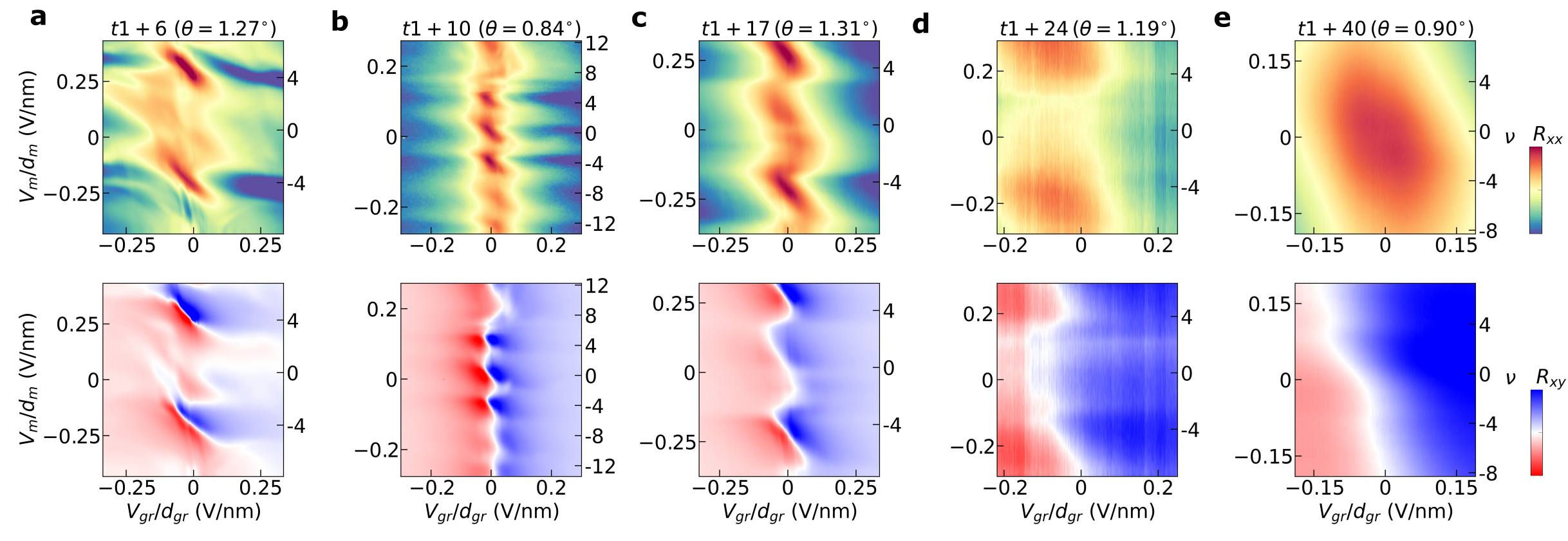
Figure 3c shows the color-coded projections from many Landau fan diagrams overlayed atop the map acquired at T. The projection point of the extended states (blue dots) oscillates with , tracking closely with the contour measured at low field for . These quantities diverge for larger values of , however, we still see occasional sharp resets in the projection point of the QOs to values near even at larger values of (e.g., at V/nm). Overall, this behavior is enabled by the unique nature of the extended standing wave states in Bernal graphite. As illustrated schematically in the top left inset of Fig. 3d, the standing wave hybridizes the moiré surface states with the graphite bulk states and inextricably mixes the properties of the two. The low- and high-field zig-zag features we see in Fig. 3c arise from distinct physical mechanisms, yet exhibit remarkably consistent behavior that is primarily determined by the total gate-induced free charge in the sample.
Unlike in Bernal graphite, the Landau fan diagrams in twisted grahene-graphite differ substantially depending on which gate is swept. In particular, we see QOs corresponding to the moiré bands only upon sweeping (Fig. 3b). We denote selected QOs projecting to full-filling of the moiré surface bands () with pink dashed lines, whereas QOs projecting to the charge neutrality point () are denoted in purple. Figure 3c shows the projection points of these states overlayed atop the map acquired at T. Again, we see good agreement between the low- and high-field features. In particular, the low-field transport around exhibits diagonal resistance features closely matching the evolution of the projection points of the high-field QOs at and . We also find that both the resistance and the QO projections depend only weakly on as the bias is raised further. These observations suggest that the moiré bands can be doped by changing when the bias is small, but that surface states on the Bernal face screen the effect of changing when the bias is large.
Despite the obvious differences in the Landau fan diagrams acquired by sweeping each gate, Brown-Zak (BZ) oscillations Brown1964 ; Hofstadter1976 ; Hunt2013 ; Dean2013 ; Ponomarenko2013 ; Kumar2017 appear in both. These occur as maxima in the magnetoconductance, , and arise at rational values of the magnetic flux filling of the moiré unit cell. The oscillations are most obvious after averaging over the entire range of each gate voltage (denoted as in Fig. 3d), thereby eliminating contributions from individual QOs at a given field. BZ oscillations are anticipated when sweeping (red curve in Fig. 3d), since charge carriers are directly populating the moiré bands. In contrast, the BZ oscillations seen upon sweeping (blue line in Fig. 3d) are more surprising, since this gate does not directly fill the moiré bands. This effect is more clearly visible in a t1+17 device with , which exhibits very sharp magnetoconductance peaks averaged over (top right inset of Fig. 3d).
The BZ oscillations correspond to conditions in which charge carriers experience zero effective magnetic field, and thus exhibit straight trajectories in real space Kumar2017 . Although it is possible for the moiré to propogate through bulk graphite due to structural relaxations, this effect has been found to arise only at ultra-small twist angles Halbertal2022 , and is therefore unlikely to be relevant in our samples. Instead, the observation of BZ oscillations upon sweeping indicates that carriers doped into the Bernal graphite surface obey transport properties dictated in part by the moiré potential on the opposite surface, providing further evidence of the hybridization of moiré and bulk states at high field. We further find that this effect persists in devices where the moiré interface is buried at the center of the sample (Extended Data Fig. 6). In this case, the moiré bands are inaccessible by gating and can not be filled by either gate, but nevertheless generate strong BZ oscillations by hybridizing with the bulk states of each rotated Bernal graphite constituent.
Discussion
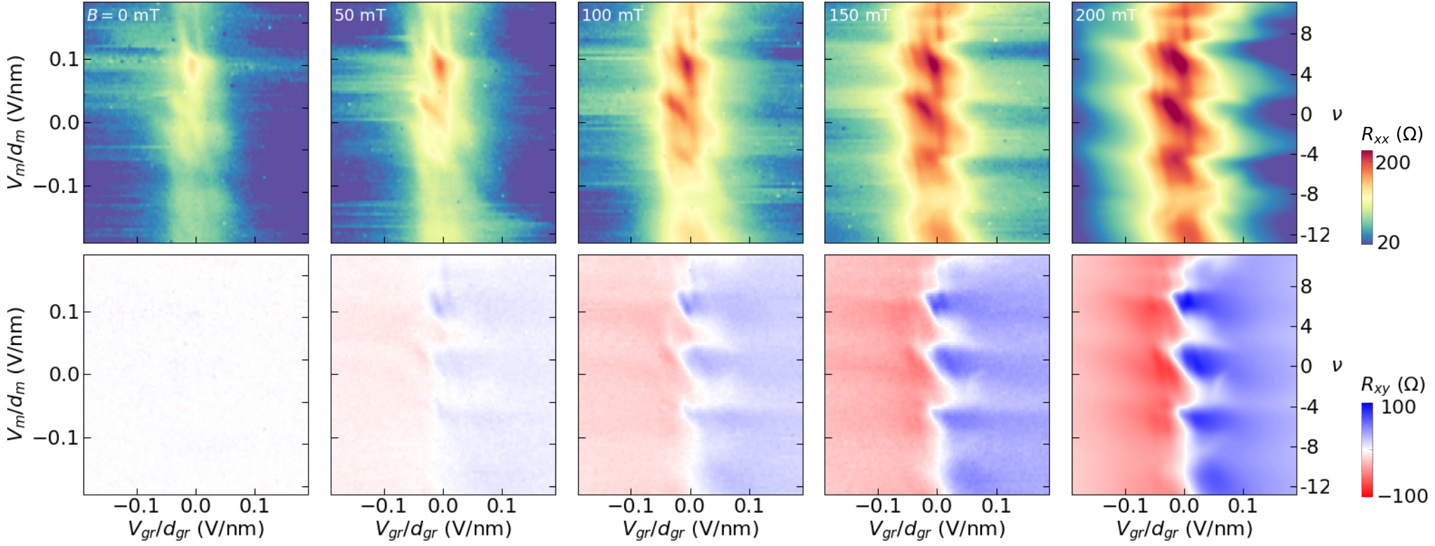
Our observations appear to be generic for t1+ graphite, as we see qualitative similarities across different graphite thicknesses and twist angles. Figure 4 shows and maps acquired at T for five samples with Bernal graphite components ranging from to layers. The zig-zag resistance feature becomes increasingly obscured for thicker graphite, but we nevertheless see oscillations in that appear to correspond closely with four-fold multiples of . The value of required to establish the complete zig-zag feature scales with the twist angle, since bias needed to fully fill the moiré surface band is directly proportional to the twist angle. In the high-field regime, we see similar zig-zag evolutions of the Landau fan diagram projections for both the t1+6 and t1+17 graphite samples (Extended Data Figs. 7 and 8 and Supplementary Videos 3-5).
Overall, our results establish a new class of ‘mixed-dimensional moiré materials,’ in which a moiré potential localized to a single 2D interface fundamentally transforms the properties of an entire bulk crystal. This behavior may generalize to other layered semimetals with low intrinsic bulk doping, in which surface accumulation layers formed by gating can dominate the transport. Similar effects could therefore arise in materials such as WTe2 and ZrTe5. Our work additionally motivates experiments with more complex graphitic structures, including those with moiré patterns at both the top and bottom surfaces and those with moiré interfaces distributed throughout the bulk of the material. At high magnetic field, standing waves in the bulk may couple these coexisting moiré potentials in interesting and exotic new ways. Finally, new complex moiré geometries in bulk graphitic thin films may help to unravel the origin of the superconductivity found both in natural few-layer graphene allotropes Zhou2021 ; Zhou2022 and in a growing family of magic-angle twisted graphene structures.
Methods
Device fabrication. Moiré devices were fabricated using the “cut-and-stack” method Chen2019a ; Saito2020 . t1+ structures are made by finding an exfoliated bulk graphite thin film with a connected monolayer graphene region, isolating the two using an atomic force microscope tip, and then stacking one atop the other at the desired twist angle. The sample with the buried moiré was made by isolating two regions from a single 7-layer graphite sheet and stacking them atop each other. All samples were assembled using standard dry-transfer techniques with a polycarbonate (PC)/polydimethyl siloxane (PDMS) stamp Wang2013 . All devices are encapsulated in flakes of BN and graphite, and then transferred onto a Si/SiO2 wafer. The temperature was kept below 180∘C during device fabrication to preserve the intended twist angle. The number of graphite layers in each device, , was determined by atomic force microscopy measurements after encapsulation. Standard electron beam lithography, CHF3/O2 plasma etching, and metal deposition techniques (Cr/Au) were used to define the complete stack into a Hall bar geometry Wang2013 .
Transport measurements. Transport measurements were performed in a Cryomagnetics variable temperature insert, and were conducted in a four-terminal geometry with a.c. current excitation of 10-200 nA using standard lock-in techniques at a frequency of 17.7 Hz. Some of the measurements acquired for the Supplementary Videos 1-2 for the t1+10 device were performed in a Bluefors dilution refrigerator at a nominal base temperature of 20 mK.
Twist angle determination. The twist angle is determined by fitting the sequence of QOs arising upon sweeping . The charge carrier density required to fill the moiré superlattice is given by , where nm. The value of is determined by tracing the QOs corresponding to full filling of the moiré surface bands to . The band filling factor, , is defined such that at doping , where the numerical factor of 4 corresponds to the spin and valley degeneracy of graphene.
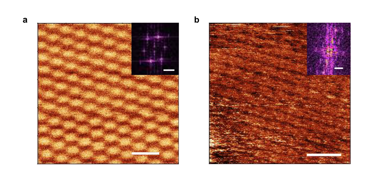
QOs projecting to full filling () are evident in all devices shown in Fig. 4 except for the t1+40 device. The twist angle for the t1+40 device was instead estimated through piezoelectric force microscopy (PFM) imaging of the moiré pattern (Extended Data Fig. 9). PFM was performed on the transfer slide during the sample fabrication directly after picking up the 40-layer graphite and the monolayer graphene McGilly2020 . The twist angle is extracted by calculating the average of the three moiré lattice points in the Fourier transform of the PFM image. The twist angle in the t1+6 device was also independently confirmed in this manner.
When observed, the BZ oscillation sequence provides an independent measure of the twist angle. Magnetoconductance peaks are expected to occur when the magnetic flux is equal to times the flux quantum , where is Planck’s constant and are integers. We extract by fitting the observed peaks to a series of rational etc. In all devices, we find that this value agrees with that extracted by tracking the QOs to within a few percent.
Temperature dependence measurements. We track the evolution of the low-field magnetotransport in the t1+17 device in Extended Data Fig. 10. We see signatures of the zig-zag feature persisting up to at least 50 K. As the temperature is raised further, the structure in the map becomes washed out. continues to exhibit a sign change, but along a straight line with a slope that becomes more vertical in the map with higher temperature. At room temperature, transport is nearly unaffected by changing , potentially due to lower mobility on the moiré surface compared to the Bernal graphite surface.
Transport model of Bernal graphite at low field. We capture the low-field transport behavior of Bernal graphite with a four-component Drude model. Magnetotransport is characterized by the conductivity tensor , with a corresponding current density under an electric field . Each of the four carrier species are independent, and have a two-dimensional carrier density denoted as , where is , , , or . In order, these correspond to the charges on the top and bottom graphite surfaces, and the intrinsic electron and hole free carriers in the graphite bulk. Each carrier species has an associated mobility, . In the absence of a magnetic field, the conductivity is a scalar and the contribution from the -th carrier is . In the presence of a magnetic field, the conductivity tensor is where the contribution from the -th carrier is
with for electrons and holes, respectively. The resistivity tensor is , where the diagonal and off-diagonal elements separately represent the longitudinal () and transverse () resistivities.
Graphite is a nearly compensated semimetal, and for simplicity we assume . We take previously measured parameters of bulk graphite Soule1958 ; McClure1958 , in which the three-dimensional bulk carrier density is and the mobility is . We assume the same value for the surface mobilities, and . The bulk electron and hole carrier densities correspond to a two-dimensional density of per graphene sheet. To model our 23-layer Bernal graphite sample, we assign 21 layers of as the fixed bulk density, . We then vary the surface density of the two remaining layers, corresponding to changing the top and bottom gate voltages over typical experimentally accessible values.
Extended Data Fig. 1a shows the results of the calculation, which qualitatively match the experimental observations in Fig. 2a. In particular, we see the largest resistivity along the line of overall charge neutrality, with a corresponding change in the sign of the Hall effect. We also see that the resistivity is largest when both of the surfaces are undoped, also consistent with our experimental results. The qualitative agreement between experiment and theory does not depend strongly on the precise values of the graphite parameters we assume. However, as an additional check, we repeat the calculation with unrealistically large bulk density, (Extended Data Fig. 1b). In this case, we find that virtually no gate dependence can be observed in the longitudinal resistivity, which changes by only tenths of an ohm, compared to over a hundred ohms in the calculation performed with realistic graphite parameters. These calculations therefore establish that the gate-tunable transport we observe in graphite arises as a consequence of its modest intrinsic bulk doping.
Band structure calculation. We first calculate the Hamiltonian for -layer Bernal graphite. We define and as the Bloch states at the point of layer . By arranging the basis as , the Hamiltonian around the point is given by
with
and
where is the electronic potential at th layer. We set the parameters eV Charlier1991 .
To calculate the band structure of twisted graphene-graphite, we further place a single graphene layer on the -layer graphite and twist it by . The effective Hamiltonian can be written as
where is the Hamiltonian for the twisted monolayer graphene. is the interlayer coupling term between the monolayer and the topmost layer of the graphite. We define and as the Bloch states of the twisted graphene at , where is the rotation matrix in the -plane at an angle . By using this basis, the Hamiltonian for the graphene can be represented as
The Bloch wavevector of the twisted graphene and the -layer graphite are coupled when , where , and , where is the moiré lattice constant. Under these constraints, the interlayer coupling is given by
and is otherwise zero. We take the parameters eV and Koshino2020 , the latter of which captures the effects of lattice relaxations.
We additionally consider the effective model for -layer graphite twisted atop -layer graphite, such that the moiré interface is buried at the center of the material. The Hamiltonian is constructed following same analysis as above, but replacing with . The two rotated graphite constituents are coupled by at their rotated interface.
We capture the effects of gating by adopting the Thomas-Fermi approximation to account for the screening of external electric fields by the graphite bulk Manes2007 ; Koshino2010 . For small gate voltages, the electric field is given by
where , and is the interlayer distance. is the potential for the moiré/graphite surface.
Finally, we numerically calculate the eigenvalues and eigenstates by truncating at a sufficiently large momentum and diagonalizing the Hamiltonian. The electron of the -th eigenvalue is distributed along the graphite -axis as follows:
where the eigenstate is written as and . and denote the width and the center of the system, respectively.
Data Availability
Source data are available for this paper. All other data that support the plots within this paper and other findings of this study are available from the corresponding author upon reasonable request.
acknowledgments
We thank D. Cobden, V. Fal’ko, S. Slizovskiy, and M. Rudner for valuable discussions. This work was supported by NSF CAREER award DMR-2041972 and NSF MRSEC 1719797. M.Y. acknowledges support from the State of Washington funded Clean Energy Institute. D.W. was supported by an appointment to the Intelligence Community Postdoctoral Research Fellowship Program at University of Washington administered by Oak Ridge Institute for Science and Education (ORISE) through an interagency agreement between the U.S. Department of Energy and the Office of the Director of National Intelligence (ODNI). E.T. and E.A-M. were supported by NSF GRFP DGE-2140004. Y.R. and D.X. were supported by the Department of Energy, Basic Energy Sciences, Materials Sciences and Engineering Division, Pro-QM EFRC (DE-SC0019443). M.F. was supported by JST CREST Grant Number JPMJCR20T3, Japan and a JSPS Fellowship for Young Scientists. K.W. and T.T. acknowledge support from the Elemental Strategy Initiative conducted by the MEXT, Japan (Grant Number JPMXP0112101001) and JSPS KAKENHI (Grant Numbers 19H05790, 20H00354 and 21H05233). This research acknowledges usage of the millikelvin optoelectronic quantum material laboratory supported by the M. J. Murdock Charitable Trust.
Author contributions
D.W., E.T. and E.A-M. fabricated the devices and performed the measurements. M.F. performed the band structure calculations. Y.R. performed the magnetotransport calculation. T.C. and D.X. supervised the calculations. K.W. and T.T. grew the BN crystals. D.W., E.T., E.A.-M. and M.Y. analyzed the data and wrote the paper with input from all authors.
Competing interests
The authors declare no competing interests.
Additional Information
Correspondence and requests for materials should be addressed to M.Y.
Supplementary Information
Supplementary Videos 1-5.
References
- (1) Balents, L., Dean, C. R., Efetov, D. K. & Young, A. F. Superconductivity and strong correlations in moiré flat bands. Nature Physics 16, 725–733 (2020).
- (2) Andrei, E. Y. & MacDonald, A. H. Graphene bilayers with a twist. Nature Materials 19, 1265–1275 (2020).
- (3) Bistritzer, R. & MacDonald, A. H. Moiré bands in twisted double-layer graphene. Proceedings of the National Academy of Sciences 108, 12233–12237 (2011).
- (4) Suárez Morell, E., Correa, J. D., Vargas, P., Pacheco, M. & Barticevic, Z. Flat bands in slightly twisted bilayer graphene: Tight-binding calculations. Physical Review B 82, 121407(R) (2010).
- (5) Cao, Y. et al. Correlated insulator behaviour at half-filling in magic-angle graphene superlattices. Nature 556, 80–84 (2018).
- (6) Cao, Y. et al. Unconventional superconductivity in magic-angle graphene superlattices. Nature 556, 43–50 (2018).
- (7) Lu, X. et al. Superconductors, orbital magnets, and correlated states in magic angle bilayer graphene. Nature 574, 653–657 (2019).
- (8) Yankowitz, M. et al. Tuning superconductivity in twisted bilayer graphene. Science 363, 1059–1064 (2019).
- (9) Park, J. M., Cao, Y., Watanabe, K., Taniguchi, T. & Jarillo-Herrero, P. Tunable strongly coupled superconductivity in magic-angle twisted trilayer graphene. Nature 590, 249–255 (2021).
- (10) Hao, Z. et al. Electric field tunable superconductivity in alternating-twist magic-angle trilayer graphene. Science 371, 1133–1138 (2021).
- (11) Park, J. M. et al. Robust superconductivity in magic-angle multilayer graphene family. Nature Materials 21, 877–883 (2022).
- (12) Burg, G. W. et al. Emergence of correlations in alternating twist quadrilayer graphene. Nature Materials 21, 884–889 (2022).
- (13) Zhang, Y. et al. Promotion of superconductivity in magic-angle graphene multilayers. Science 377, 1538–1543 (2022).
- (14) Chen, S. et al. Electrically tunable correlated and topological states in twisted monolayer–bilayer graphene. Nature Physics 17, 374–380 (2021).
- (15) Polshyn, H. et al. Electrical switching of magnetic order in an orbital chern insulator. Nature 588, 66–70 (2020).
- (16) Shi, Y. et al. Tunable van hove singularities and correlated states in twisted monolayer-bilayer graphene. Nature Physics 17, 619–626 (2021).
- (17) He, M. et al. Competing correlated states and abundant orbital magnetism in twisted monolayer-bilayer graphene. Nature Communications 12, 4727 (2021).
- (18) Shen, C. et al. Correlated states in twisted double bilayer graphene. Nature Physics 16, 520–525 (2020).
- (19) Liu, X. et al. Tunable spin-polarized correlated states in twisted double bilayer graphene. Nature 583, 221–225 (2020).
- (20) Cao, Y. et al. Tunable correlated states and spin-polarized phases in twisted bilayer–bilayer graphene. Nature 583, 215–220 (2020).
- (21) Burg, G. W. et al. Correlated insulating states in twisted double bilayer graphene. Physical Review Letters 123, 197702 (2019).
- (22) He, M. et al. Symmetry breaking in twisted double bilayer graphene. Nature Physics 17, 26–30 (2021).
- (23) Cea, T., Walet, N. R. & Guinea, F. Twists and the electronic structure of graphitic materials. Nano Letters 19, 8683–8689 (2019).
- (24) Li, G. et al. Observation of van hove singularities in twisted graphene layers. Nature Physics 6, 109–113 (2010).
- (25) Soule, D. E. Magnetic field dependence of the hall effect and magnetoresistance in graphite single crystals. Phys. Rev. 112, 698–707 (1958).
- (26) McClure, J. W. Analysis of multicarrier galvanomagnetic data for graphite. Phys. Rev. 112, 715–721 (1958).
- (27) Koshino, M. Interlayer screening effect in graphene multilayers with and stacking. Phys. Rev. B 81, 125304 (2010).
- (28) Yin, J. et al. Dimensional reduction, quantum hall effect and layer parity in graphite films. Nature Physics 15, 437–442 (2019).
- (29) McClure, J. W. & Spry, W. J. Linear magnetoresistance in the quantum limit in graphite. Phys. Rev. 165, 809–815 (1968).
- (30) Hofstadter, D. R. Energy levels and wave functions of bloch electrons in rational and irrational magnetic fields. Physical Review B 14, 2239 (1976).
- (31) Brown, E. Bloch electrons in a uniform magnetic field. Phys. Rev. 133, A1038–A1044 (1964).
- (32) Hunt, B. et al. Massive dirac fermions and hofstadter butterfly in a van der waals heterostructure. Science 340, 1427–1430 (2013).
- (33) Dean, C. R. et al. Hofstadter’s butterfly and the fractal quantum hall effect in moire superlattices. Nature 497, 598–602 (2013).
- (34) Ponomarenko, L. A. et al. Cloning of dirac fermions in graphene superlattices. Nature 497, 594–597 (2013).
- (35) Kumar, R. K. et al. High-temperature quantum oscillations caused by recurring bloch states in graphene superlattices. Science 357, 181–184 (2017).
- (36) Halbertal, D. et al. Multi-layered atomic relaxation in van der waals heterostructures. arXiv:2206.06395 (2022).
- (37) Zhou, H., Xie, T., Taniguchi, T., Watanabe, K. & Young, A. F. Superconductivity in rhombohedral trilayer graphene. Nature 598, 434–438 (2021).
- (38) Zhou, H. et al. Isospin magnetism and spin-polarized superconductivity in bernal bilayer graphene. Science 375, 774–778 (2022).
- (39) Chen, G. et al. Evidence of a gate-tunable mott insulator in a trilayer graphene moiré superlattice. Nature Physics 15, 237–241 (2019).
- (40) Saito, Y., Ge, J., Watanabe, K., Taniguchi, T. & Young, A. F. Independent superconductors and correlated insulators in twisted bilayer graphene. Nature Physics 16, 926–930 (2020).
- (41) Wang, L. et al. One-dimensional electrical contact to a two-dimensional material. Science 342, 614–617 (2013).
- (42) McGilly, L. J. et al. Visualization of moiré superlattices. Nature Nanotechnology 15, 580–584 (2020).
- (43) Charlier, J.-C., Gonze, X. & Michenaud, J.-P. First-principles study of the electronic properties of graphite. Physical Review B 43, 4579 (1991).
- (44) Koshino, M. & Nam, N. N. T. Effective continuum model for relaxed twisted bilayer graphene and moiré electron-phonon interaction. Physical Review B 101, 195425 (2020).
- (45) Mañes, J. L., Guinea, F. & Vozmediano, M. A. H. Existence and topological stability of fermi points in multilayered graphene. Phys. Rev. B 75, 155424 (2007).
Extended Data


Supplementary Videos
Supplementary Video 1. (left) Landau fan diagrams from the t1+10 device acquired by sweeping at the indicated values of . Selected QOs are denoted at the top of the image by black and blue arrows, with the corresponding projection points at indicated by black and blue dots. Some arrows correspond to QOs that are only visible at intermediate values of in the map (i.e., QOs that do not directly connect to the arrow itself). We note that there are many other visible QOs not indicated by arrows, all of which appear to project either to the black or blue dots. The black and blue dots are chosen by judging the best fit for the entire sequence of visible QOs. In general, the blue dots align with the value of corresponding to the highest resistance over a wide range of in the map. (right) map acquired at T with the corresponding black and blue dots overlayed.
Supplementary Video 2. (left) Landau fan diagrams from the t1+10 device acquired by sweeping at the indicated values of . Selected QOs are denoted at the top of the image by pink and purple arrows, with the corresponding projection points at indicated by pink and purple dots. Some arrows correspond to QOs that are only visible at intermediate values of in the map (i.e., QOs that do not directly connect to the arrow itself). We note that there are many other visible QOs not indicated by arrows, all of which appear to project the pink and purple dots. The pink and purple dots are chosen by judging the best fit for the entire sequence of visible QOs. (right) map acquired at T with the corresponding pink () and purple ( dots overlayed.
Supplementary Video 3. Same as Supplementary Video 1, but for the t1+6 device.
Supplementary Video 4. Same as Supplementary Video 2, but for the t1+6 device.
Supplementary Video 5. Same as Supplementary Video 1, but for the t1+17 device. This video only includes Landau fans with . The fans acquired for were taken only up to due to technical constraints in those particular measurements, and are not included in the video for the sake of continuity. Nevertheless, these lower-field fans still enable unambiguous QO projections, as plotted on the map.