Synthesis of Modulated Dielectric Metasurfaces for Precise Antenna Beamforming
Abstract
This paper presents an end-to-end design method for the synthesis of dielectric metasurfaces with modulated thickness that are able to realize desired radiation patterns in the far-field with high precision. The method relies on integral equations and the Method of Moments to calculate the induced surface and volumetric current densities throughout the metasurface upon a given incident illumination. By avoiding homogenization of the dielectric layer and calculating directly the scattered fields through the Method of Moments, the near-field and far-field response of the metasurface can be accurately predicted and optimized. In particular, a design example of a modulated dielectric metasurface, fed by a single embedded line source, is presented for the realization of a Chebyshev array pattern with sidelobe level. Moreover, an externally-fed dielectric metasurface performing beam splitting of a normally-incident plane wave is designed, 3-D printed and measured, showing two reflected beams at , high suppression of specular reflections () and satisfactory agreement with the simulated and desired radiation patterns. The proposed design method for beamforming with dielectric metasurfaces can find application in higher frequencies where the use of copper may be problematic due to higher ohmic losses and fabrication challenges.
I Introduction
Metasurfaces have demonstrated significant potential in manipulating electromagnetic waves in ways beyond the ones observed in natural material interfaces. Typically, metasurfaces take the form of subwavelength polarizable particles that are arranged in an electromagnetically thin sheet [1, 2, 3, 4]. These particles excite secondary co-located electric and magnetic dipole moments which scatter secondary fields, as envisioned by the Huygens’ principle. By engineering locally the response to the incident illumination, a number of useful functionalities have been observed with the use of metasurfaces, including perfect anomalous refraction [5, 6], perfect anomalous reflection [7, 8, 9], antenna beamforming [10, 11, 12, 13], and polarization control [14, 15].
The subwavelength dimensions of the scatterers comprising the metasurface allow its homogenization and its mathematical modelling with effective macroscopic surface parameters. These have been expressed in the literature in different forms, such as the effective surface polarizabilities, the surface susceptibilities or the surface impedances/admittances [16, 17, 18]. Following the underlying homogenization procedure, the design usually consists of two distinct steps. First, the macroscopic parameters are determined based on the input illumination and the desired functionality. Secondly, the homogenized parameters are implemented by appropriately designing the scattering elements.
Lately, a number of works have been presented where the macroscopic design relies on a set of integral equations that accurately predict the scattered fields from the metasurface structure [19, 20, 21]. By iteratively solving the integral equations through a Method of Moments (MoM) [22], it is possible to optimize one or more homogenized impedance layers to achieve a desired electromagnetic response from the metasurface. This full-wave optimization method captures the mutual coupling between all the metasurface scatterers, allowing for precise control of the near-field or far-field region. On the contrary, previous methods that represent the metasurface as an infinitesimally thin boundary and rely on the implementation of each discretized cell sometimes suffer from coupling between adjacent elements. While vias have been proposed as baffles between cells to suppress coupling effects, this approach increases fabrication challenges and it is practically applicable only to the transverse-magnetic (TM) polarization [23].
At microwave frequencies, metasurfaces commonly consist of one or more copper layers etched on standard dielectric substrates. Although the resonant nature of metallic scatterers allows for compact metasurface structures, it is also associated with increased losses, sensitivity to fabrication imperfections and limited bandwidth. Moreover, at higher frequencies, etching tolerances (e.g., minimum trace size) can become a limiting factor and require very delicate etching procedures. In these cases, dielectric-based metasurfaces could lead to designs that are less lossy, more broadband and easier to fabricate. In particular, the fabrication of dielectric metasurfaces is greatly facilitated by the advancements of 3-D printing technology, as 3-D printing materials with relatively low losses (e.g., Acrylonitrile Butadiene Styrene - ABS) can be easily printed in arbitrary shapes at a low cost [24, 25, 26].
Dielectric metasurfaces have been utilized in the past to realize beams based on the holographic approach [27, 28]. The structure, consisting of a grounded corrugated dielectric, supports a single surface-wave mode that gradually converts to leaky-wave radiation by applying a slowly-varying modulation in the equivalent homogenized surface impedance. The surface impedance, then, translates locally to the corresponding height of the dielectric based on a transmission-line model. Some control of the radiation characteristics can be achieved by optimizing locally the modulation coefficient, that controls the intensity of surface-wave to leaky-wave conversion [29]. On the other hand, a recent work treated the design of impenetrable dielectric metasurfaces by optimizing the induced auxiliary surface waves to render a single homogenized impedance layer passive and lossless [30]. It has been shown that these passively-induced surface waves are necessary to redistribute the incident power and achieve full phase and amplitude control with a passive metasurface [31, 32, 33]. However, in [30], the implementation of the optimized impedance layer with a thickness-modulated dielectric layer resulted to sub-optimal performance (compared to the same design with copper-based metasurfaces) due to the unaccounted coupling effects. Finally, a sparse dielectric metasurface controlling the reflected Floquet-Bloch (F-B) modes has been proposed; yet, the approach can only be applied to periodic metasurfaces with a relatively small number of propagating F-B modes [34].
In this work, we focus on the design of thickness-modulated dielectric metasurfaces to realize desired radiation patterns in the far-field region. The design is based on the optimization of the shape of the metasurface using integral equations solved with the MoM. Notably, the optimization scheme avoids homogenization completely, and, therefore, the derivation of an approximate relation between a homogenized surface impedance and the local height of the metasurface is not necessary. Moreover, all mutual coupling effects are considered and there is no assumption of local periodicity when determining the heights of each segment. This allows realizing beams with high-accuracy and desired characteristics both with an internal and an external illumination of the metasurface. Finally, the method can easily be extended to design dielectric metasurfaces that handle multiple inputs and produce multiple corresponding outputs. All examples are verified by commercial full-wave simulation solvers and a prototype for beam splitting in reflection mode is 3-D printed and measured.
The rest of the paper is organized as follows. Section II.1 presents the geometry and mathematical formulation to analyze the structure through a set of integral equations. The optimization scheme and applied constraints are also described. A design example of a dielectric metasurface with an embedded source is discussed in Sec. III. Section IV deals with the case of external illumination and a beam splitter is designed for a normally incident plane wave. Moreover, the fabrication details and the measurements to experimentally verify the design are presented. Lastly, Sec. V concludes the paper.
II Analysis and synthesis framework
In this section, we present the general geometry of thickness-modulated metasurfaces and the rigorous mathematical analysis of such structures through integral equations combined with the MoM approach. Subsequently, we introduce the optimization scheme to synthesize dielectric metasurfaces based on a desired far-field radiation pattern.
II.1 Geometry
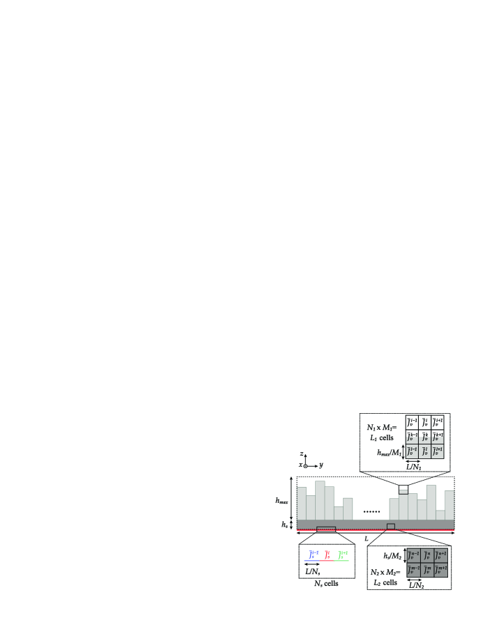
The geometry under consideration consists of a thickness-modulated dielectric layer of relative permittivity , an optional fixed-thickness dielectric layer of relative permittivity and an underlying ground plane, as shown in Fig. 1. The fixed dielectric layer has a thickness of and it can serve as a low-loss standard substrate for an embedded source, if the metasurface is internally illuminated. The structure has a total length of along the -dimension, while it is assumed to extend infinitely along the -axis to simplify our analysis. In practice, such uniformity along the -axis can be established, even if we truncate the metasurface at around ( being the free-space wavelength), as will be shown in simulations and experiments. The modulated layer is divided in segments with varying heights . The purpose of this work is to optimize the heights to obtain the desired far-field radiation. As mentioned, the incident field can either be produced by an embedded source, or it can refer to an incident wave illuminating the metasurface externally. In the latter case, the fixed dielectric layer can be omitted and the modulated layer is placed directly above the ground plane.
II.2 Analysis through Integral Equations
To be able to optimize thickness-modulated dielectric metasurfaces, as the one shown in Fig. 1, we first need to solve the analysis problem, i.e., to predict the scattering of the structure upon some kind of incident illumination. We base our analysis on a set of integral equations similar to [20], with the main difference being that there is no homogenized impedance layer in the present work, but only a ground plane and a dielectric region . We assume that the incident electromagnetic wave is transverse-electric (TE) polarized for simplicity . Together with the uniformity of the structure along the -axis, it follows that the scattered fields would also be TE polarized and we can simply analyze a cross-section of the structure. Finally, a time-harmonic dependance is assumed for the electromagnetic quantities throughout the manuscript.

The incident field will induce a surface current density along the ground plane and a polarization volumetric current density in the dielectric region , where is the position vector in the -plane. In turn, the induced current densities produce secondary scattered fields and , respectively. Since the dielectric is modelled with a polarization current, the corresponding scattered fields are calculated based on the -D free-space Green’s function as follows:
| (1a) | ||||
| (1b) | ||||
where is the zero-order Hankel function of the second kind, and are the observation and source position vectors, respectively, and is the free-space wavenumber. From Eqs. (1), it is evident that calculating the scattered fields from the metasurface reduces to determining the unknown induced current densities .
The total electric field is formed through the superposition of the incident field and the additional scattered fields and . The total electric field should be zero at the ground plane (as it is tangential to it) and it should satisfy Ohm’s law in the dielectric region:
| (2) |
where is the angular frequency of the wave, is the free-space permittivity and is the position-dependant dielectric constant. In particular, the region refers to the whole rectangular region that can be potentially be filled up with the thickness-modulated dielectric. Based on the geometry of Fig. 1, this means that could take the values of , or unity, depending on whether the observation point is in the modulated dielectric, the fixed dielectric or the air-filled region. In the latter case, the proportionality constant between the electric field and the volumetric current density becomes infinite, essentially indicating that there is no induced current in air.
Equations (1) and (II.2) form a set of integral equations with respect to the unknown current densities that we treat with the MoM. Specifically, the surface and volumetric current densities are expanded to non-overlapping -D and -D pulse basis function, respectively. The grid employed is illustrated in Fig. 2. As observed, there are pulse basis functions on the ground plane corresponding to the surface current density. Similarly, there are pulse basis functions for the modulated-layer dielectric region and for the fixed-layer dielectric region. The total number of basis functions along in the modulated dielectric, denoted by , is set to be an integer multiple of the number of segments , so that no cell is shared between two consecutive segments.
After expansion of the current densities to the basis functions, point matching is employed at the center of each -D or -D cell defined previously. This results in a linear system of equations of the following form:
| (3) |
where are matrices representing the self and mutual interactions between the different areas of the dielectric metasurface, are the current amplitudes of the pulse pulse basis functions covering each cell and is the incident field values at the center of each cell. The expressions for the elements of the matrices are given in the Appendix A. Finally, is a diagonal matrix of size with the elements calculated as
| (4) |
where is the dielectric constant value at each cell. For a particular set of heights , some cells may fall entirely within the dielectric region (), some within the air region () and some may intersect the interface between the modulated dielectric and air. For these intersecting cells, an averaged value based on the percentage of each region is assigned as the value of the cell. This is important for facilitating the optimization of the heights , since a smooth variation of the heights will result in a smooth variation of the averaged in the cells of the interface and, as a result, an approximate, but smooth variation of the induced currents and the far-field radiation. On the contrary, assigning, for instance, the dielectric constant value of the middle of the cell could result to identical results for small variations of heights causing the optimization scheme to stop prematurely.
Solving the system in Eq. (3) determines the induced currents and across the metasurface for a specified set of heights . Then, the far-field electric field and the radiation intensity at different angles can be computed as a superposition of the radiation from all the induced currents and from the incident source. The analytic expressions for this step are omitted, but they can be found in [20].
II.3 Synthesis through Optimization
After treating the analysis problem in Sec. II.2, the next step is to utilize it to form a synthesis optimization scheme that determines the heights of each segment in the modulated dielectric layer in order to achieve a desired electromagnetic functionality. The aim of this paper is to realize beams with desired far-field patterns in the -plane. Naturally, a cost function needs to quantify the difference between the desired radiation intensity and the one obtained for a dielectric metasurface with a set of heights . Because the total power of the desired radiation intensity may differ from the available power from the source, the cost function takes a normalized form as follows:
| (5) |
where is a set of equally spaced angles across the upper half space (). It is also noted that radiation intensities and are given in linear scale.
To minimize the cost function in Eq. (5) different optimization methods may be used. In this work, we utilize the built-in genetic algorithm of MATLAB, followed by gradient descent optimization. In general, a global optimization algorithm as the first step explores better the multivariable space of heights compared to the gradient descent that heavily depends on the initial point. On the other hand, gradient descent is utilized as a second step of the overall optimization, as it quickly converges to the (local) minimum around the initial solution. The pseudo-random nature of the seed in the genetic algorithm results in different solutions with every run of the optimization. Therefore, for challenging design cases, the combined optimization scheme can be ran multiple times and the best solution (the one corresponding to the minimum in Eq. (5)) is recorded.
Constraints can be introduced to converge to solutions that are practically realizable and have high performance metrics. In particular, the heights are constrained in the interval in order for the metasurface to have structural support while maintaining compactness. Moreover, by allowing the dielectric constant to be complex, the power losses and the total radiated power can be predicted during optimization, as:
| (6) | ||||
| (7) |
Therefore, a constraint on the power efficiency can be placed fostering the convergence to solutions that exhibit less losses compared to the ones produced from unconstrained optimization, while they realize nearly identical radiation patterns. Typically, this means that lower-amplitude surface waves are excited to the vicinity of the metasurface in order to redistribute the incident power.
Finally, it is worth mentioning that the speed of our optimization scheme depends heavily on the inversion of the matrix in Eq. (3). To accelerate this process, we use the Kron reduction technique, as outlined in [20]. Based on this technique we can rearrange the equations in (3) to form a system of size , that corresponds to the portion of the matrix that potentially changes at each iteration, as it depends on the cells of the thickness-modulated layer. Additionally, the rows and lines of the matrix corresponding to the air-filled cells can be discarded at each iteration, because there is no induced current in these cells, reducing the size of the inverted matrix further to only a portion of .
III Internally-fed dielectric Metasurface
In this section, we present the design of thickness-modulated dielectric metasurface illuminated by an embedded source. The structure has the form illustrated in Fig. 1 with a total length of in the operating frequency of . The modulated dielectric is divided in segments with minimum height and maximum height . The fixed-thickness layer has a height of and supports a line source located at . We assume realistic dielectric constants of for the fixed layer (close to the properties of ABS or other machinable dielectric materials) and for the fixed layer (as provided, for example, for Rogers RO3003). The aim is to realize a Chebyshev radiation pattern with a sidelobe level (SLL) of . To determine the pattern , we first assume an array of virtual current line sources placed along the -axis at a distance between them and with currents calculated according to a Chebyshev antenna array [35]. Then, the radiation pattern is simply the array factor of this linear non-uniform array.

For the discretization grid required for the MoM framework, we use basis functions for the ground plane, for the modulated thickness layer (, ) and for the fixed layer (,). Moreover, the far-field mismatch is minimized at a total of angles at the interval . Given that the incident field and the desired radiation pattern are symmetric along the -axis, we also enforce this symmetry in the heights of the segments , essentially reducing the optimization variables in half. Lastly, we constrain the power efficiency to . The resulting optimized heights are plotted in Fig. 3.
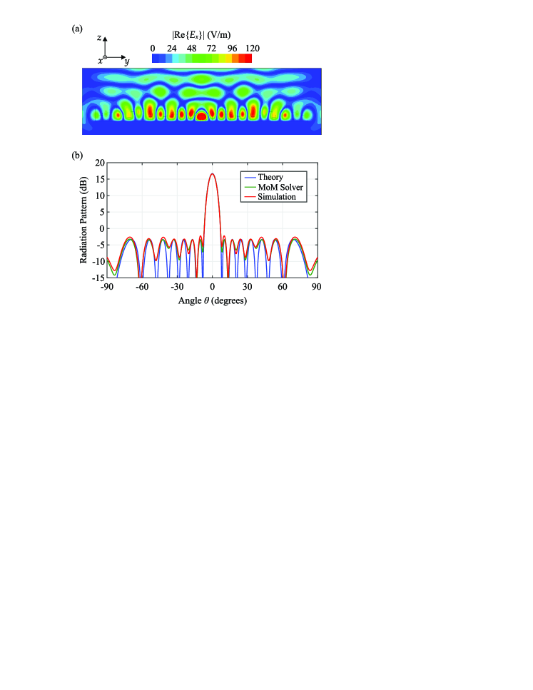
We verify our framework by a full-wave simulation in Ansys High Frequency Structure Simulator (HFSS). As seen from the Fig. 4(a), the incident power is redistributed along the dielectric metasurface and gradually leaks, forming a planar wavefront traveling towards with a tapered amplitude corresponding to the Chebyshev pattern. The far-field radiation from the simulation is given in Fig. 4(b), and it is compared with the results from our MoM solver and with the desired theoretical radiation pattern. Evidently, all of them match quite well in terms of the main beam, the null positions and the sidelobe levels. In particular, the obtained results from simulation differ by only from the desired pattern regarding the maximum directivity, while the SLL is kept at or lower. The power efficiency coincided with the constraint of for the solution of the MoM solver, and it is in the HFSS simulation, limited primarily by the high-field values in the dielectric region close to the embedded source. Finally, the drop in the broadside directivity remains within -dB compared to the nominal frequency for the range of . This indicates a relative bandwidth, which is higher compared to copper-based metasurfaces with similar functionality [20].
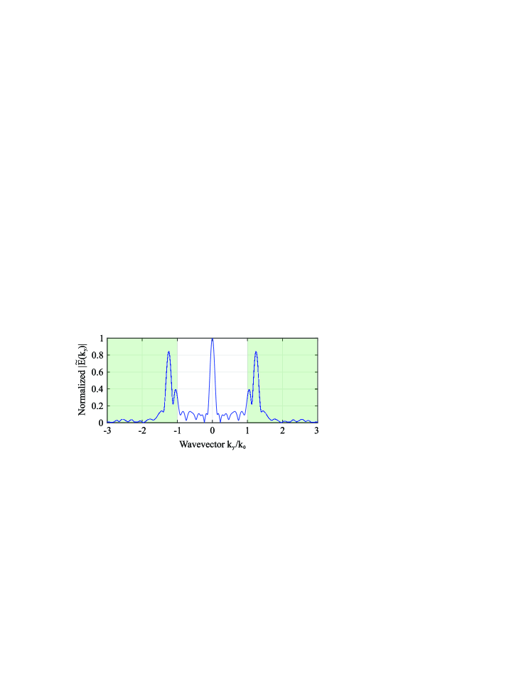
It is worth examining the spectrum of the electric field in the vicinity of the dielectric metasurface. Specifically, we record the total electric field at the plane (around above the maximum height of the structure) and calculate its spatial spectrum components. The spectral amplitude is depicted in Fig. 5, where clearly a strong evanescent spectrum () is observed. These surface waves effectively redistribute the input power from the localized source towards the edges of the dielectric metasurface. Moreover, it is shown that an optimization targeting for a specific aperture field above the metasurface (in the near-field region) would be constraining for our far-field applications. This is because the near-field may contain strong evanescent waves that affect the electric field values and are not known a priori, but they are still necessary to achieve the amplitude tapering and desired far-field radiation pattern.
IV Externally-fed dielectric metasurface
In this section, we discuss the design, fabrication and measurement of a thickness-modulated dielectric metasurface which is illuminated externally by a normally-impinging plane wave. Since there is no need for an embedded source, the fixed dielectric layer in Fig. 1 is omitted and the modulated dielectric is placed directly above the ground plane. The metasurface has a length of at the frequency of of the incident wave. This length is partitioned to segments, each with a width of (or ) and a height ranging between and . The desired reflected fields are two superimposed plane waves radiating at with equal power in each one of them. To determine the desired far-field , we assume two superimposed sets of virtual current line sources across the ground plane, each with uniform amplitude and linear phase:
| (8) |
where are the virtual sources positions, imposes the equal power-splitting and is selected as a phase detuning between the two beams for optimal sidelobe level. The far-field is calculated as the total radiation from these virtual sources.
The dielectric constant of the modulated-thickness layer needs to be determined based on the available 3D-printable material; in our case, a standard ABS filament. For this purpose, we 3-D printed rectangular cuboids of solid ABS with their lateral dimensions fitting the cross-section of a WR-90 rectangular waveguide. By measuring the -parameters of the waveguide with and without the samples, and using analytical expressions from the transmission through a lossy slab, we are able to deduce the values for the dielectric constant. Specifically, an average value of is extracted from the phase of at and a loss tangent of is estimated from the losses . In any case, a small offset of the dielectric permittivity does not affect significantly the expected radiation pattern for our design. In the Supplemental Material, we include a number of supporting graphs showing the sensitivity of the optimized design to variations of the dielectric permittivity, the truncation of the metasurface along the -axis and the wavefront of the illuminating wave [36].
The optimization is performed with a discretization grid of basis functions for the ground plane and basis functions for the dielectric area (), while the radiation pattern is matched at angles at the interval . The power efficiency is constrained at to avoid solutions that exhibit high field concentration within the lossy dielectric. The optimized heights after convergence are shown in Fig. 6.

The optimized dielectric metasurface is 3-D printed with ABS in a Modix Big-60 3-D printer using a nozzle size of and infill percentage for the dielectric. Moreover, the metasurface is truncated to along the -axis for fabrication, since this was proven sufficient in full-wave simulations to obtain a nearly-identical radiation pattern, when comparing with the infinite case. After fabrication, a copper-cladded substrate of the same dimensions is attached at the back of the dielectric to act as the underlying ground plane. A photo of the fabricated prototype is given in Fig. 7(a).

The metasurface is measured in an anechoic chamber with the use of two identical X-band pyramidal horn antennas, as shown in Fig. 7(b). Both horn antennas are placed at a distance of from the stage holding the metasurface, ensuring that the transmitting antenna illuminates the metasurface with a planar wavefront and that the receiving antenna is recording values in the far-field region. The transmitting antenna is at a fixed location with its axis normal to the metasurface, while the receiving antenna rotates at a constant radius with the help of a moving tripod and a rotating pipe connecting the tripod to the stage.
The measured radiation pattern of the reflected fields, is given in Fig. 8. Moreover, we have included the radiation pattern measurement of the copper base without the modulated dielectric (negative angles were mirrored for this measurement due to symmetry) and the simulated pattern from HFSS. Regarding the measurements, the receiving antenna physically collides with the transmitting antenna when their angular separation is less than . However, since the two antennas have the same gain and are placed at the same distance from the stage, we use the value of for the measurement directly at broadside (instead of the which is used for all other angles). We also normalize all measured values with respect to the broadside reflections of the bare copper plate. Finally, the simulation pattern is also normalized with respect to the theoretical value of the radiation pattern at from a perfect conducting plate of the same size illuminated by a normally-incident plane wave.

As observed in Fig. 8, two beams with the maximum intensity at and appear at the measured radiation pattern. Moreover, the specular reflections () are suppressed by more than , when comparing the thickness-modulated metasurface with the bare copper plate. Generally, the pattern matches quite well the one predicted from simulation, especially when considering fabrication imperfections and the resolution of our bi-static measurement setup. Specifically, for the fabrication there was a slight warping for part of the metasurface, rendering its base non-flat and creating a non-uniform small air gap between the dielectric and the copper plate. This could be addressed in future designs by optimizing further the temperature settings for the 3-D printer or by fabricating the dielectric structure in smaller pieces before attaching them to the copper base.
The peaks of the measured pattern are only below the simulation results. The observed difference includes both the drop due to the non-ideal pattern and also the power losses, which already account for () in the simulation, assuming the extracted loss tangent . This demonstrates that indeed the dielectric beam-splitter exhibits quite low losses, a metric cared for through the constraints in the optimization phase. Lastly, to quantify the bandwidth of our reflective beam-splitting metasurface, we record the measured gain for the peaks at and . The drop compared to the value in is less than for the frequency range of , while the same applies for the range in the simulation results.
While, we presented here a relatively simple example of symmetric beam splitting to experimentally verify the proposed method, the design opportunities of our MoM framework are vast, and they can include metasurfaces that manipulate multiple inputs to produce multiple desired outputs. A description of optimizing for such a design case and the corresponding simulation results are included in the Supplemental Material [36].
V Conclusion
In conclusion, we present a design framework for dielectric metasurfaces with varying thickness for realizing desired radiation patterns. The method avoids homogenization techniques employed in previously designed corrugated dielectric metasurfaces. On the contrary, it is based on integral equations which accurately predict the induced current upon some incident illumination. In the first presented example, the illumination is coming from an embedded source and the metasurface radiates waves with a Chebyshev radiation pattern in the far-field region. Full-wave simulations verified the good matching with the desired pattern in terms of the directivity and the sidelobe level of . Next, an example with an externally-illuminated dielectric metasurface was presented for beam-splitting in reflective mode. This design was verified by 3-D printing such a prototype and performing measurements with a bi-static measurement setup. The experimental results showed beam-splitting at the desired angles of with high suppression of specular reflections and low power losses. The proposed end-to-end design framework, resulting in dielectric metasurfaces that can be directly fabricated with 3-D printing technology, offers beamforming capabilities and it can be advantageous in cases that copper-based metasurfaces are lossy, costly or hard to fabricate. Such beamforming functionalities with the use of dielectric metasurfaces can be utilized in existing and emerging technologies, such as 6G communication links, antenna radomes and dielectric cloaking coatings among others.
Appendix A Mathematical expressions for the Method of Moments solution
For the MoM solution, the surface and volume electric current densities in Eqs. (1) are expanded to a set of pulse basis functions with constant amplitudes and , respectively. The centers of the pulse basis functions for the ground plane are located at and for the dielectric cells at , with the subscript extending up to the total number of the corresponding cells. Then, point matching is applied at the center of each 1-D or 2-D cell, which is equivalent to taking the inner product with a delta function to both sides of Eq. (II.2), based on:
| (9) |
where refers to the ground plane and dielectric cells, respectively. Based on this, a system of equations is obtained that is written in matrix form in Eq. (3).
Here, expressions for the elements of the matrices in Eq. (3) are given. For the non-diagonal elements () of the matrix and for all elements of matrix , using the midpoint rule (with a single interval), we have:
| (10) | |||
| (11) |
where , are the position vectors corresponding to the discretizing pulse basis function (source points) and the point matching locations (observation points), respectively and is the width of each discretized segment in the ground plane. The diagonal terms of the matrix are given based on a small argument approximation for the Hankel function (Eq. (3.14),[22]):
| (12) |
where is the Euler’s number.
For the matrices and , where the source point refers to the 2-D dielectric cells, the approximation introduced in [37] is used, which treats the 2-D rectangular source cell as a circular cell of equal area. Using this approximation, the following expressions can be derived for the matrix elements:
| (13) | |||
| (14) |
where is the first-order Bessel function, is the first-order Hankel function of the second kind, and is the radius of a circle with area equal to the size of the 2-D rectangular dielectric cell with dimensions .
References
- Yu et al. [2011] N. Yu, P. Genevet, M. A. Kats, F. Aieta, J.-P. Tetienne, F. Capasso, and Z. Gaburro, Light propagation with phase discontinuities: Generalized laws of reflection and refraction, Science 334, 333 (2011).
- Holloway et al. [2012] C. L. Holloway, E. F. Kuester, J. A. Gordon, J. O’Hara, J. Booth, and D. R. Smith, An overview of the theory and applications of metasurfaces: The two-dimensional equivalents of metamaterials, IEEE Antennas Propag. Magazine 54, 10 (2012).
- Pfeiffer and Grbic [2013] C. Pfeiffer and A. Grbic, Metamaterial Huygens’ surfaces: Tailoring wave fronts with reflectionless sheets, Phys. Rev. Lett. 110, 197401 (2013).
- Selvanayagam and Eleftheriades [2013] M. Selvanayagam and G. V. Eleftheriades, Discontinuous electromagnetic fields using orthogonal electric and magnetic currents for wavefront manipulation, Opt. Express 21, 14409 (2013).
- Lavigne et al. [2018] G. Lavigne, K. Achouri, V. S. Asadchy, S. A. Tretyakov, and C. Caloz, Susceptibility derivation and experimental demonstration of refracting metasurfaces without spurious diffraction, IEEE Trans. Antennas Propag. 66, 1321 (2018).
- Chen et al. [2018] M. Chen, E. Abdo-Sánchez, A. Epstein, and G. V. Eleftheriades, Theory, design, and experimental verification of a reflectionless bianisotropic Huygens’ metasurface for wide-angle refraction, Phys. Rev. B 97, 125433 (2018).
- Ra’di et al. [2017] Y. Ra’di, D. L. Sounas, and A. Alù, Metagratings: Beyond the limits of graded metasurfaces for wave front control, Phys. Rev. Lett. 119, 067404 (2017).
- Wong and Eleftheriades [2018] A. M. H. Wong and G. V. Eleftheriades, Perfect anomalous reflection with a bipartite Huygens’ metasurface, Phys. Rev. X 8, 011036 (2018).
- Rabinovich et al. [2019] O. Rabinovich, I. Kaplon, J. Reis, and A. Epstein, Experimental demonstration and in-depth investigation of analytically designed anomalous reflection metagratings, Phys. Rev. B 99, 125101 (2019).
- Epstein and Eleftheriades [2017] A. Epstein and G. V. Eleftheriades, Arbitrary antenna arrays without feed networks based on cavity-excited omega-bianisotropic metasurfaces, IEEE Trans. Antennas Propag. 65, 1749 (2017).
- Raeker and Grbic [2019] B. O. Raeker and A. Grbic, Compound metaoptics for amplitude and phase control of wave fronts, Phys. Rev. Lett. 122, 113901 (2019).
- Dorrah and Eleftheriades [2018] A. H. Dorrah and G. V. Eleftheriades, Bianisotropic Huygens’ metasurface pairs for nonlocal power-conserving wave transformations, IEEE Antennas Wireless Propag. Lett. 17, 1788 (2018).
- Ataloglou and Eleftheriades [2021] V. G. Ataloglou and G. V. Eleftheriades, Arbitrary wave transformations with Huygens’ metasurfaces through surface-wave optimization, IEEE Antennas Wireless Propag. Lett. 20, 1750 (2021).
- Niemi et al. [2013] T. Niemi, A. O. Karilainen, and S. A. Tretyakov, Synthesis of polarization transformers, IEEE Trans. Antennas Propag. 61, 3102 (2013).
- Selvanayagam and Eleftheriades [2014] M. Selvanayagam and G. V. Eleftheriades, Polarization control using tensor Huygens surfaces, IEEE Trans. Antennas Propag. 62, 6155 (2014).
- Kuester et al. [2003] E. F. Kuester, M. A. Mohamed, M. Piket-May, and C. L. Holloway, Averaged transition conditions for electromagnetic fields at a metafilm, IEEE Trans. Antennas Propag. 51, 2641 (2003).
- Achouri et al. [2015] K. Achouri, M. A. Salem, and C. Caloz, General metasurface synthesis based on susceptibility tensors, IEEE Trans. Antennas Propag. 63, 2977 (2015).
- Epstein and Eleftheriades [2016] A. Epstein and G. V. Eleftheriades, Arbitrary power-conserving field transformations with passive lossless omega-type bianisotropic metasurfaces, IEEE Trans. Antennas Propag. 64, 3880 (2016).
- Budhu and Grbic [2021] J. Budhu and A. Grbic, Perfectly reflecting metasurface reflectarrays: Mutual coupling modeling between unique elements through homogenization, IEEE Trans. Antennas Propag. 69, 122 (2021).
- Xu et al. [2022] G. Xu, V. G. Ataloglou, S. V. Hum, and G. V. Eleftheriades, Extreme beam-forming with impedance metasurfaces featuring embedded sources and auxiliary surface wave optimization, IEEE Access 10, 28670 (2022).
- Budhu et al. [2022] J. Budhu, E. Michielssen, and A. Grbic, The design of dual band stacked metasurfaces using integral equations, IEEE Trans. Antennas Propag. 70, 4576 (2022).
- Harrington [1993] R. F. Harrington, Field Computation by Moment Methods (Wiley-IEEE Press, 1993).
- Xu et al. [2019] G. Xu, S. V. Hum, and G. V. Eleftheriades, Augmented Huygens’ metasurfaces employing baffles for precise control of wave transformations, IEEE Trans. Antennas Propag. 67, 6935 (2019).
- Pepino et al. [2018] V. M. Pepino, A. F. da Mota, A. Martins, and B.-H. V. Borges, 3-D-printed dielectric metasurfaces for antenna gain improvement in the ka-band, IEEE Antennas Wireless Propag. Lett. 17, 2133 (2018).
- Poyanco et al. [2021] J.-M. Poyanco, F. Pizarro, and E. Rajo-Iglesias, 3D-printed dielectric grin planar wideband lens antenna for 5G applications, in 2021 15th European Conf. Antennas Propag. (EuCAP) (2021) pp. 1–4.
- Cheng et al. [2022] Q. Cheng, Y. Hao, J. McGhee, W. G. Whittow, J. C. Vardaxoglou, R. Mittra, and S. Zhang, Dual circularly polarized 3-D printed broadband dielectric reflectarray with a linearly polarized feed, IEEE Trans. Antennas Propag. 70, 5393 (2022).
- Minatti et al. [2010] G. Minatti, F. Caminita, and S. Maci, A circularly polarized dielectric lens antennas designed by holographic principle, in 2010 IEEE Antennas and Propagation Society International Symposium (2010) pp. 1–4.
- Minatti et al. [2011] G. Minatti, F. Caminita, M. Casaletti, and S. Maci, Spiral leaky-wave antennas based on modulated surface impedance, IEEE Trans. Antennas Propag. 59, 4436 (2011).
- Puggelli et al. [2015] F. Puggelli, G. Minatti, Y. Vardaxoglou, and S. Maci, Design of a modulated dielectric metasurface antenna, in 2015 Loughborough Antennas Propagation Conference (2015) pp. 1–3.
- Lee and Kwon [2021] H. Lee and D.-H. Kwon, Large and efficient unidirectional plane-wave–surface-wave metasurface couplers based on modulated reactance surfaces, Phys. Rev. B 103, 165142 (2021).
- Epstein and Eleftheriades [2016] A. Epstein and G. V. Eleftheriades, Synthesis of passive lossless metasurfaces using auxiliary fields for reflectionless beam splitting and perfect reflection, Phys. Rev. Lett. 117, 256103 (2016).
- Kwon and Tretyakov [2018] D.-H. Kwon and S. A. Tretyakov, Arbitrary beam control using passive lossless metasurfaces enabled by orthogonally polarized custom surface waves, Phys. Rev. B 97, 035439 (2018).
- Ataloglou and Eleftheriades [2020] V. G. Ataloglou and G. V. Eleftheriades, Surface-waves optimization for beamforming with a single omega-bianisotropic Huygens’ metasurface, in Proc. IEEE Int. Symp. Antennas Propag. North Amer. Radio Sci. Meeting (2020) pp. 905–906.
- Sharma and Wong [2021] A. Sharma and A. M. Wong, Dimer dielectric Huygens’ metasurface: Realizing perfect anomalous reflection at 60 ghz, in Proc. IEEE Int. Symp. Antennas Propag. North Amer. Radio Sci. Meeting (2021) pp. 203–204.
- Balanis [2016] C. A. Balanis, Antenna Theory: Analysis and Design, 4th ed. (John Wiley and Sons, 2016).
- [36] See Supplemental Material at for a sensitivity analysis of the beam-splitting metasurface discussed in Sec. IV and for a design example of a dual-input dual-output modulated dielectric metasurface that anomalously reflects two incident waves at two desired directions.
- Richmond [1965] J. Richmond, Scattering by a dielectric cylinder of arbitrary cross section shape, IEEE Trans. Antennas Propag. 13, 334 (1965).