Scanning gate microscopy in graphene nanostructures
Abstract
The conductance of graphene nanoribbons and nanoconstrictions under the effect of a scanning gate microscopy tip is systematically studied. Using a scattering approach for noninvasive probes, the first- and second-order conductance corrections caused by the tip potential disturbance are expressed explicitly in terms of the scattering states of the unperturbed structure. Numerical calculations confirm the perturbative results, showing that the second-order term prevails in the conductance plateaus, exhibiting a universal scaling law for armchair graphene strips. For stronger tips, at specific probe potential widths and strengths beyond the perturbative regime, the conductance corrections reveal the appearance of resonances originated from states trapped below the tip. The zero-transverse-energy mode of an armchair metallic strip is shown to be insensitive to the long-range electrostatic potential of the probe. For nanoconstrictions defined on a strip, scanning gate microscopy allows to get insight into the breakdown of conductance quantization. The first-order correction generically dominates at low tip strength, while for Fermi energies associated with faint conductance plateaus, the second-order correction becomes dominant for relatively small potential tip strengths. In accordance with the spatial dependence of the partial local density of states, the largest tip effect occurs in the central part of the constriction, close to the edges. Nanoribbons and nanoconstrictions with zigzag edges exhibit a similar response as in the case of armchair nanostructures, except when the intervalley coupling induced by the tip potential destroys the chiral edge states.
I Introduction
Graphene has established itself as a unique platform for revealing new physical features since it was discovered Novoselov et al. (2004, 2005), due to the electron pseudorelativistic dispersion and its exceptional high mobilities. Its two-dimensional carbon atom lattice leads to a gapless linear dispersion at low energies, and the corresponding electrons, so-called massless Dirac fermions, can be described in the low-energy regime by a two-dimensional Dirac equation Castro Neto et al. (2009). Understanding the underlying principles of electronic transport properties of high-mobility graphene nanostructures in the quantum coherent regime is of significant basic interest, as well as crucial for future nanoelectronics applications Peres (2010). A variety of experimental techniques have been employed in this quest, among them, scanning gate microscopy (SGM), originally applied to the two-dimensional electron gas (2DEG) in the vicinity of a quantum point contact (QPC) defined on a semiconductor heterojunction Topinka et al. (2000).
In the SGM technique, a probe, consisting of a metallized atomic force microscope (AFM) tip, perturbs the sample local electrostatic potential, while electron transport is measured. The provided spatial resolution of the tip-position-dependent conductance gives additional information regarding coherent transport, beyond that gained in a standard transport measurement Sellier et al. (2011). The 2DEG that forms in the intrinsically two-dimensional structure of graphene is particularly suited for scanning probe techniques. Several groups have used SGM in order to detect localized charges Schnez et al. (2010); Pascher et al. (2012); Garcia et al. (2013) and charge inhomogeneities Jalilian et al. (2011) in graphene samples. Moreover, SGM techniques have been employed to image the electronic cyclotron orbits in graphene Morikawa et al. (2015); Bhandari et al. (2016) and scarred wave functions Cabosart et al. (2017), as well as to probe conductance fluctuations Berezovsky et al. (2010) and weak localization Berezovsky and Westervelt (2010); Chuang et al. (2016) for coherent transport in graphene.
An early application to a narrow constriction in a graphene flake Neubeck et al. (2012) demonstrated that SGM can be used to investigate graphene nanostructures, showing that the conductance is considerably affected when the tip is at the position of the narrowing. More recent systematic experiments on micrometer-sized constrictions Brun et al. (2019); Guerra (2021) showed that the phenomenon of Klein tunneling considerably modifies the effect of the tip, and can lead to the possibility of Veselago lensing induced by the -- landscape that appears in the presence of the tip-induced potential. The SGM has also been used to manipulate quantum Hall edge channels Xiang et al. (2016); Bours et al. (2017) and to study the topological breakdown of the quantum Hall effect at the edges of graphene constrictions Moreau et al. (2021); Moreau (2022).
The theoretical study of the Veselago effect in the vicinity of a graphene nanoconstriction (GNC) has been addressed with ray-tracing approaches and tight-binding calculations Guerra (2021); Moreau (2022), while the magnetic focusing observed with SGM in graphene samples in Refs. Morikawa et al. (2015); Bhandari et al. (2016) has been analyzed with the aid of quantum simulations Petrović et al. (2017). Numerical calculations have also been employed in a very thorough investigation of the SGM response in graphene nanoribbons (GNRs) and GNCs with different geometrical features Mreńca et al. (2015); Mre (2022); Mreńca-Kolasińska and Szafran (2017). Within this context, it is important to develop a theoretical approach to the SGM response in order to address the generality of parameter regimes and geometries that can be experimentally encountered. Therefore, in this work, we systematically study the effect of a tip-induced potential on the conductance of graphene nanoribbons with and without an additional constriction. In particular, we generalize the perturbation theory valid in the regime of noninvasive tips Jalabert et al. (2010); Gorini et al. (2013) to the situation of graphene and deduce the conductance corrections that appear in low orders of the tip strength. Numerical tight-binding simulations are used to test the limits of these predictions and to address the regime of invasive tips.
We introduce electronic transport in those systems in Sec. II and the description of the tip potential in Sec. III. The perturbative approach for low tip strength is presented in Sec. IV, and the results are discussed together with numerically obtained data for armchair edges, including for the nonperturbative regime of invasive tips, in Secs. V and VI. The case of zigzag edges is discussed in Sec. VII. After the conclusions (Sec. VIII), three appendixes describe technical details of the perturbative approach.
II Electronic transport in graphene nanoribbons and nanocontacts
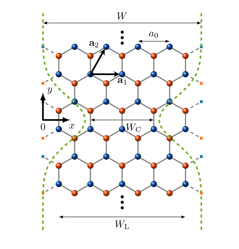
We choose to characterize the graphene honeycomb structure by the primitive lattice vectors and , with and the nearest-neighbor distance. With the convention adopted in Fig. 1, the two atoms (indicated by blue and red dots) of the conventional cell are located at and . The associated first Brillouin zone, defined by the reciprocal vectors and , has two inequivalent corners at and .
We describe the electron motion in the - plane through a nearest-neighbor tight-binding model taking into account the orbitals of the carbon atoms, with a hopping constant . Within such a model, low-energy physics is described by a Hamiltonian with two Dirac points located at the and points of the first Brillouin zone and where the two components of the pseudospinor correspond to the values of the wave function at the two sublattices. These two valleys (Dirac cones), with a linear pseudorelativistic dispersion relation and a (Fermi) velocity , are independent in bulk graphene, but they are coupled through the boundary conditions in the finite-size samples that we are interested in. Within this work we perform numerical calculations using the kwant code Groth et al. (2014), adopting the tight-binding model to constrained geometries, and we use analytical approaches based on the low-energy description of pseudorelativistic electrons.
The simplest structure to approach the study of coherent electronic transport in graphene is a quasi-one-dimensional strip, that is, a GNR connected to electronic reservoirs (source and drain). The quest to fabricate atomically precise GNRs Lin et al. (2008); Jiao et al. (2009); Lian et al. (2010); Cai et al. (2010); Baringhaus et al. (2014); Rizzo et al. (2020) was initiated soon after the pioneering isolation of graphene monolayers Novoselov et al. (2004), while their theoretical characterization in the context of graphite studies Nakada et al. (1996) predated the previous experimental achievements. In particular, the electronic and transport properties of perfect GNRs have been shown to depend on the atomic arrangement at the edges of the strip Brey and Fertig (2006); Wurm et al. (2009); Yamamoto et al. (2009); Wakabayashi et al. (2010); Wurm et al. (2012); Bergvall (2014); Cao et al. (2017), and to be strongly affected by defects Muñoz Rojas et al. (2006); Li and Lu (2008); Mucciolo et al. (2009); Ihnatsenka and Kirczenow (2009); Orlof et al. (2013). Considerable progress has been achieved in the fabrication procedures since the diffusive strips that first showed signs of subband quantization formation Lin et al. (2008); Lian et al. (2010), and it is nowadays possible to fabricate very narrow (of the order of in width) GNRs with atomic precision and specific armchair or zigzag edges Ruffieux et al. (2016); Kolmer et al. (2020) (although quantum transport measurements seem for now challenging for these very small samples). For a recent review on GNRs, see Ref. Wang et al. (2021).
Within the convention of Fig. 1, cutting the edges of the strip along the direction gives rise to an armchair GNR, while cutting along the axis results in a zigzag GNR (not shown). In the case of an armchair GNR the wave function vanishes on both sublattices at the edges, while for a zigzag GNR the wave function vanishes on a single sublattice at each edge. Denoting the width of the graphene strip, we define the effective width for convenience. In Appendix A we present the electronic eigenstates of armchair nanoribbons, which provide a useful basis for the scattering approach to quantum transport through graphene nanostructures and for the perturbative development of the SGM response.
In our study of quantum transport we consider the linear regime, where a small applied source-drain bias voltage results in a small current , and we focus on the linear conductance at zero temperature. Assuming that the scatterer is connected to two leads that can be assimilated to semi-infinite nanoribbons with propagating modes labeled by the channel index , the two-terminal Landauer formula reads
| (1) |
where is the quantum of conductance and the matrix elements of the transmission amplitude matrix evaluated at the Fermi energy .
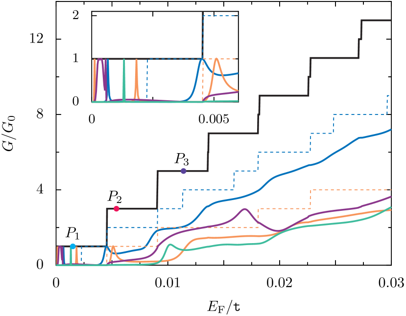
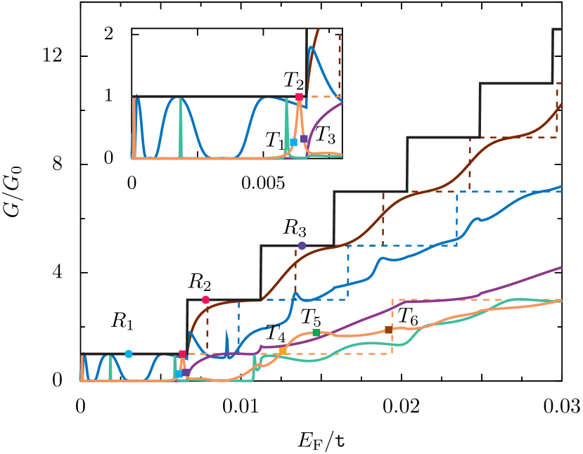
An infinite GNR provides an example of a perfect scatterer, with a unitary transmission for all the propagating modes. Thus, is a steplike function of the Fermi energy . In Fig. 2 we present the numerical results for the conductance of a metallic armchair nanoribbon with a width (where electron transport is along the vertical direction ) as a function of the Fermi energy (thick black solid line). The zero-transverse-energy mode, not being degenerate, determines the first conductance plateau at . Upon increasing , the other modes become progressively populated. The Dirac equation predicts these modes to be doubly degenerate, and thus conductance plateaus are separated by steps of . The numerical results agree with such an expectation for small values of , but as increases, lattice effects become relevant, the mode degeneracy is progressively destroyed, and plateaus with steps of start to appear.
As commented above, the conductance quantization obtained in a perfect GNR, like that of Fig. 2, is not robust, since a moderate amount of edge roughness results in an important suppression of the conductance and the appearance of localized states at the edges Muñoz Rojas et al. (2006); Li and Lu (2008); Mucciolo et al. (2009); Ihnatsenka and Kirczenow (2009). The sensitivity is most pronounced near the neutrality point, where the number of propagating modes is small. By the same token, the definition of a nanoconstriction in a GNR considerably deteriorates the conductance quantization. Indeed, a hallmark of mesoscopic physics, the conductance quantization with plateaus at integer multiples of observed in transport through semiconductor-based QPCs van Wees et al. (1988); Wharam et al. (1988), is elusive in GNCs, where no well-defined plateaus are typically observed, particularly for sharp constrictions.
The signatures of conductance quantization observed in high-quality suspended Tombros et al. (2011) or hexagonal-boron-nitride encapsulated Terrés et al. (2016) devices were reproducible modulations (kinks) in the conductance with a spacing that varies in the range of to . The differences with the clear quantization characteristic of semiconductor-based QPCs were attributed to strong short-range scattering at the rough edges of the device Kinikar et al. (2017) favoring the intervalley coupling. The use of nanopatterning techniques allowed to define GNCs with high precision and reduced edge roughness, resulting in a more robust quantization Kun et al. (2020). Depending on the geometry and the smoothness of the edges, spikes in the conductance might appear due to the resonances associated with the finite length of the constriction Clericò et al. (2018).
Conductance quantization in semiconductor QPCs can be understood from the adiabatic electron transport, in the case of a smooth constriction with a slow variation in the transverse dimension Glazman et al. (1988); *glazman1998JETP, or alternatively, from the small mismatch between the transmission eigenmodes in the leads and the propagating channels within the junction, in the case of abrupt geometries Szafer and Stone (1989). Both adiabaticity and small mismatch are problematic in GNCs, resulting in a poor observed conductance quantization. For the case of zigzag edges, the adiabatic approximation fails to describe the constriction region, since the electron motion along the stripe is strongly coupled with that in the perpendicular direction, while for armchair edges the change of edge orientation along the constriction is a source of scattering Katsnelson (2007). Unlike a semiconductor QPC, the GNC appears as a short-range scatterer, which, together with other possible defects, degrades the conductance quantization.
A million-atom simulation of smooth constrictions resulted in faint quantization steps in integers of , put in evidence by a clustering of dips in around these conductance values Ihnatsenka and Kirczenow (2012). The conductance spikes obtained in geometries like that of Ref. Clericò et al. (2018) were linked to the longitudinal quantization induced by the finite length of the constriction Yannouleas et al. (2015).
We choose for our model calculations a smooth GNC geometry described by the condition
| (2) |
which is illustrated by the green dashed lines in Fig. 1, where is the narrowest width and characterizes the length of the constriction. Nonzero values of the electronic wave function are allowed only on lattice sites that fulfill condition (2). The details of the constriction geometry are known to be determinant for its transport properties. Depending on the fabrication procedure, we may have wedgelike constrictions Terrés et al. (2016) or smooth structures Tombros et al. (2011). Our choice (2) of a smooth GNC for the SGM calculations is motivated by its simplicity, and the fact that by varying the two defining parameters and , the degree of abruptness can be tuned.
In agreement with the results of Ref. Ihnatsenka and Kirczenow (2012), Fig. 2 shows that the presence of a constriction reduces the transmission of the ribbon and destroys the conductance plateaus. The thick colored solid lines show the conductance of GNCs of different width () and length () of the constriction. For each of the two values of chosen, the conductance of a GNR with that width is presented by thin dashed lines with the corresponding color, i.e., dark blue (orange) for (). These values represent the conductance that would have a perfectly adiabatic constriction characterized by the width . Since both widths define a semiconductor armchair GNR, a zero-conductance region appears at low energy, and for larger the conductance plateaus are separated by steps of . Only for very short GNCs (, violet line), tunneling across the constriction permits to exceed, at specific energies, the limit set by the corresponding fictitious GNR. The conductance resonances appearing at low Fermi energy, shown on smaller scale in the inset of Fig. 2, have been observed in other numerical simulations Ihnatsenka and Kirczenow (2012); Mreńca et al. (2015); Guimarães et al. (2012); Yannouleas et al. (2015), and they can be attributed to quasi-bound states in a GNC Xiong and Xiong (2011); Deng et al. (2014).
An insight into the origin of the faint conductance plateaus of GNCs can be obtained by working in the representation of the transmission eigenmodes (i.e., the eigenvectors of ) Jalabert (2016), for which the Landauer formula (1) becomes a diagonal sum,
| (3) |
where the are referred to as the transmission eigenvalues associated to the transmission eigenmodes . In the upper panel of Fig. 3 we reproduce the dependence of the conductance presented in Fig. 2 for and (thick dark blue line), decomposed according to the contribution of the transmission eigenvalues (thin colored lines). We see that as increases, different transmission eigenmodes are progressively turned on, and at some point they approach unitary transmission, which favors the appearance of faint plateaus with an approximately quantized conductance.
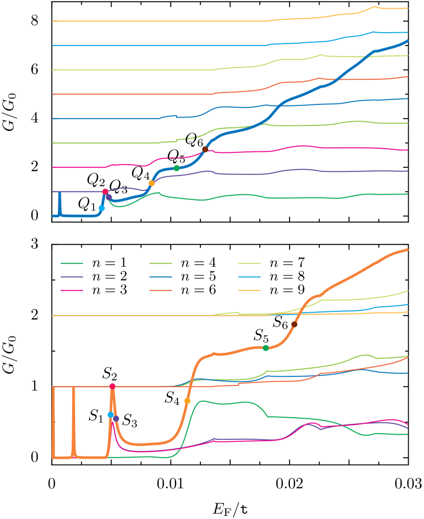
The lower panel of Fig. 3 shows the eigenmode decomposition for the case of another GNC considered in Fig. 2, with and (thick orange line), being more abrupt than the one of the upper panel. The transmission eigenmodes are also turned on upon increasing , and when they attain an approximately constant value, the resulting conductance presents a faint plateau. However, the abruptness of this constriction results in transmission eigenvalues with some nonmonotonic dependence on without achieving the unitary limit. Therefore, the conductance plateaus are less well defined than in the previous case, and farther away from the quantized values. Another special feature of the second example above is that the and eigenmodes are degenerate up to , with the same transmission eigenvalue.
As we will see in the sequel, the transmission eigenmode representation greatly helps to understand the SGM response. The latter is strongly dependent on the value of the unperturbed conductance. Parameters used for a detailed study of the SGM response are indicated in Figs. 2 and 3 by the points and or for GNRs and GNCs, respectively.
III SGM in graphene nanostructures
In an SGM setup the electronic conductance is measured while the charged tip of an AFM is scanned over the sample. The electrostatic potential induced by the tip at the level of the two-dimensional graphene electrons can be approximated by a Lorentzian function Mreńca-Kolasińska and Szafran (2017); Brun et al. (2019, 2020); Moreau (2022), and thus we write the corresponding potential energy as
| (4) |
where stands for the projection of the tip position on the graphene plane, while the potential strength and the disturbance width are related to the voltage applied to the tip and on the distance between the tip and the graphene flake, respectively. Since is typically much larger than the lattice spacing , the perturbing potential can be taken as a scalar (i.e., the same for both sublattices and without inducing a coupling between them). In experiments, the value of is limited by the distance of the tip to the graphene sheet, and is then often of the order of Brun et al. (2019). In order to limit technical issues due to tip potentials extending beyond the system into the leads, we choose smaller values in our theoretical approach, yet at least an order of magnitude larger than .
As we will show in Sec. V, there is no SGM correction for the zero-transverse-energy mode. Therefore, we present in Fig. 4 a typical SGM scan, plotting the numerically obtained response (defined as the conductance of the sample with the tip minus the one without) in units of the conductance quantum , as a function of the tip position for the case of a metallic armchair nanoribbon (with ), for a Fermi energy that places the unperturbed conductance in the second plateau (point of Fig. 2).
The SGM scan of Fig. 4 appears as translationally invariant in the longitudinal direction, despite two effects that break this symmetry. On the one hand, the lattice-induced symmetry breaking in the direction produces conductance modulations that are imperceptible within the chosen scale. On the other hand, cutting the tip-potential tail at the leads results in a finite-size effect that we minimize by simulating a strip which is more than seven times longer than the sector shown.
While many features of quantum transport through graphene nanostructures can be inferred from the scans like that of Fig. 4, the large number of physical parameters involved indicate that a systematic approach must be pursued. In the next section we develop a perturbative approach accounting for the SGM response of Dirac electrons in graphene to a noninvasive tip potential, that will guide our discussion of the SGM results upon different conditions.
IV Perturbative approach for noninvasive tips
The effect of a noninvasive tip can be obtained from perturbation theory following the same lines as in the case of the 2DEG Jalabert et al. (2010); Gorini et al. (2013). We present in this section the main steps of the approach, while technical details can be found in Appendixes A and C.
The Dyson equation for the total Green function (including the effect of the tip) can be written in terms of the unperturbed Green function and the tip-induced potential as
| (5) |
Staying up to first order in (i.e., within the Born approximation) and using the Fisher-Lee relation (36), the correction to the transmission amplitude can be written as
| (6) |
where we have skipped its explicit dependence, used the spectral decomposition (33) of the unperturbed Green functions, and defined the matrix element of the tip potential between scattering states
| (7) |
In Appendix B we present explicit calculations for the case where the system is a GNR [see Eqs. (41) and (44)].
Assuming a smooth dependence of the tip-potential matrix elements on and , expressing the scattering states in terms of the modes , and using the result (45), we have
| (8a) | ||||
| (8b) | ||||
Therefore,
| (9) |
and we obtain the first-order correction to the conductance
| (10) |
which has the same form as in the case of the 2DEG Jalabert et al. (2010). Expressing the conductance correction as a trace, analogously to the Landauer formula (1), makes it manifestly independent of the basis chosen for the lead states. The basis of the transmission eigenmodes is quite useful since it allows to write Eq. (10) as a single sum over the propagating eigenmodes Gorini et al. (2013)
| (11) |
where () is the transmission (reflection) eigenvalue and is the diagonal matrix element of the tip potential in the basis of the transmission eigenmodes. The case of a strip is particularly simple since the lead modes (31) are the transmission eigenmodes.
It follows directly from Eq. (10) that there is no first-order correction for the perfectly transmitting modes. In these cases, which include that of the GNRs, we need to go beyond the first-order approximation in order to address the SGM response. The second-order SGM conductance correction can be written as
| (12) |
with
| (13a) | ||||
| (13b) | ||||
Going up to second order in Eq. (IV) we have
| (14) |
The result of the sum and integral of the above equation follows from Eq. (8a), and similarly, the sum and integration from Eq. (8b), leading to
| (15) |
We thus have
| (16) |
where we have used that is real. The correction can be readily obtained from Eqs. (13b) and (9), leading to
| (17) |
From and we obtain the second-order conductance correction
| (18) |
As for the first-order correction, the representation of transmission eigenmodes considerably simplifies the above expression, since the traces can be calculated as single sums. In the case where all the propagating eigenmodes are perfectly transmitting, as in GNRs, Eq. (IV) reduces to
| (19) |
This second-order correction to the conductance in the case of perfect transmission is trivially negative (or null), respecting the constraint that the presence of the tip cannot open additional conductance channels in the leads, but only reduce the transmission of the existing channels.
V SGM correction in a metallic armchair graphene nanoribbon
We first tackle the geometry of a nanoribbon, which is particularly simple since the perfect transmission of the propagating modes results in a vanishing first-order conductance correction, i.e., according to Eq. (10). Therefore, the second-order term , given by Eq. (19), is the leading-order correction for a noninvasive probe. Moreover, in the case of armchair GNRs, the tip-potential matrix elements can be calculated under some approximations (see Appendix B). For the case of and distances from the tip to the boundaries larger than , the matrix element (41) is independent of the tip position, resulting in
| (20) |
where the sum is over the propagating modes , and stands for the zeroth-order modified Bessel function of the second kind.
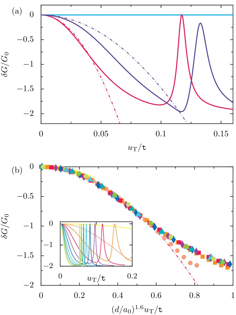
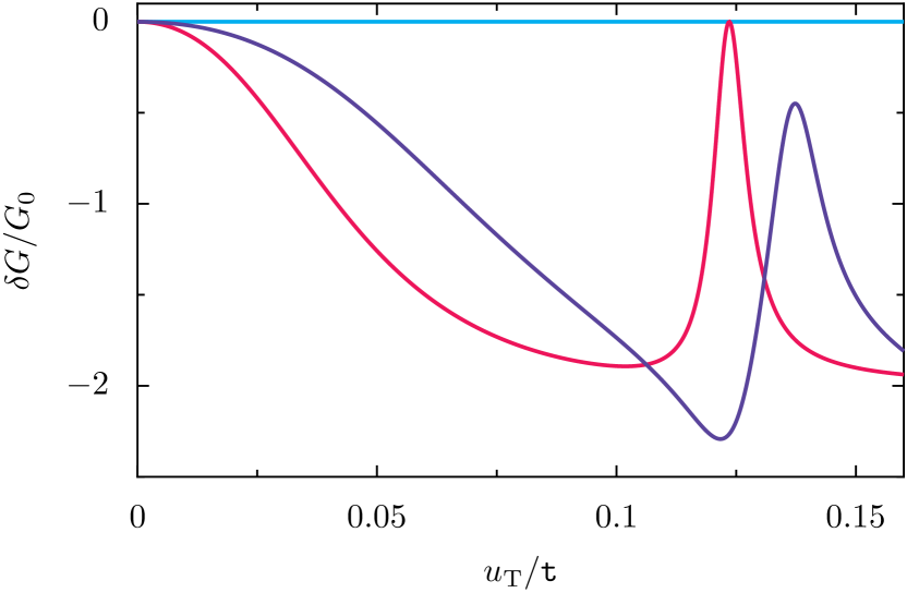
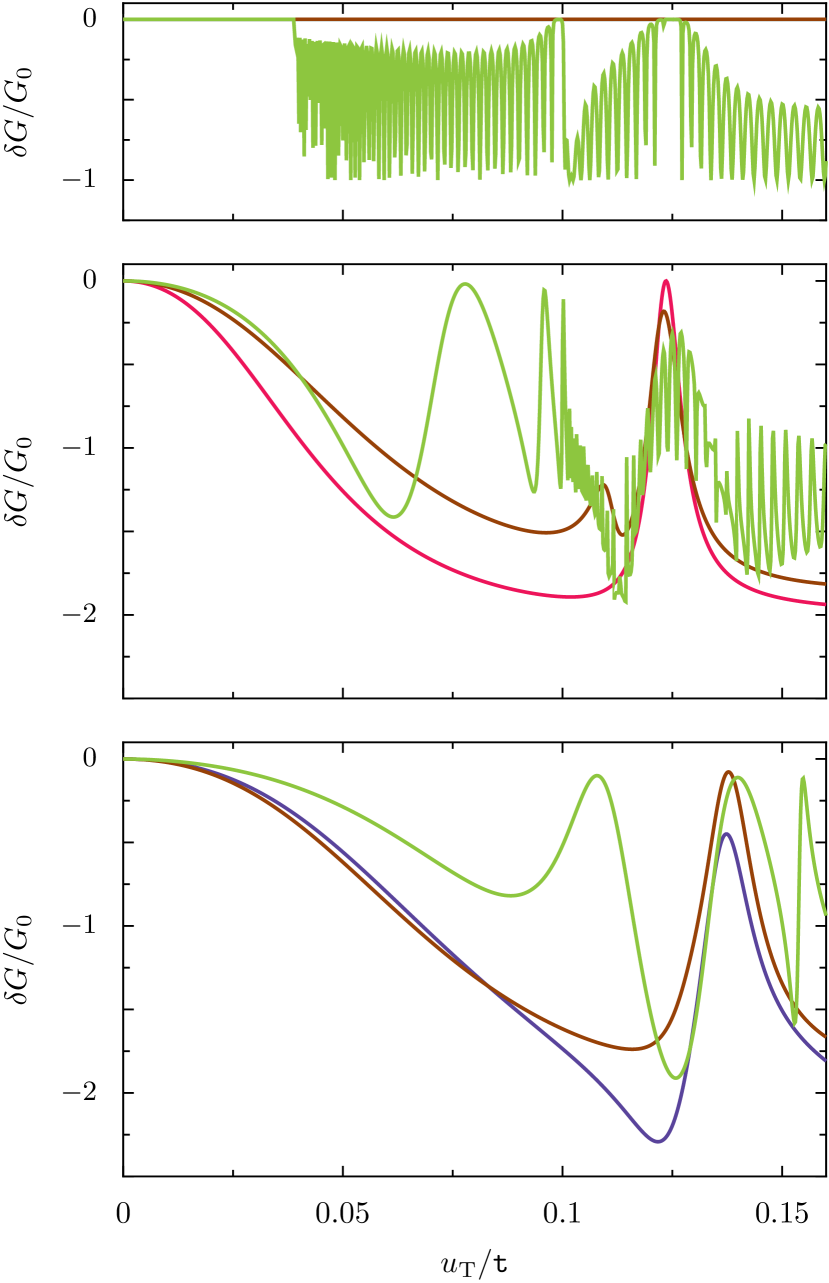
In Fig. 5(a), we present the numerically obtained SGM correction as a function of the tip strength (scaled by the hopping constant ) when the tip of fixed size is placed on the axis of the strip (at with the coordinate system of Fig. 1) for three cases where the unperturbed conductance is in the first (blue solid line), second (red solid line), and third (purple solid line) plateau (points , , and of Fig. 2, respectively).
The first remarkable feature is that when only the zero-transverse-energy mode is occupied, the SGM correction vanishes on the scale of the other curves (typically, ). This singularity, already noticed in Ref. Mreńca et al. (2015); *Mre_ca_Kolasi_ska_2022, is consistent with Eq. (20), which dictates that the second-order conductance correction trivially vanishes in this case. Moreover, as we stress in Appendix B, it can be shown that , without introducing all the approximations that lead to Eq. (20), and independently of the characteristics of the tip potential ( and ), provided it is long ranged. The result is indeed valid for an arbitrary long-range disorder potential. This leads to the concept of nearly perfect single-channel conduction for armchair GNRs Yamamoto et al. (2009), as the higher-order terms in the perturbation expansion cannot in principle be ruled out, since other matrix elements do not vanish [see Eq. (44)]. Invoking the time-symmetry breaking operated by the boundary conditions in the case of metallic armchair GNRs, Ref. Wurm et al. (2012) proposed that the zero-transverse-energy mode in armchair GNRs is a perfectly conducting channel.
The distinction between a perfectly conducting channel and a nearly perfect conducting one is delicate from the numerical point of view Wurm et al. (2012). Indeed, the small values of in Fig. 5(a) are affected by the finite-size effects due to the long-range tip potential extending up to the leads in our simulations with a finite extent along the direction, as well as by the fact that the potential of the numerical calculations has a finite range and therefore mixes the graphene valleys. However, from the theoretical point of view, the perfect conduction of the zero-transverse-energy channel can be addressed by going to higher order in the perturbation expansion.
For the zero-transverse-energy mode, the first corrections to the transmission amplitude are easily obtained from Eqs. (9), (15), and (48), resulting in and . It is easy to see that the th-order correction to the transmission amplitude has the same structure as Eq. (15), with intermediate energy integrals and sums over the lead index, and having products of matrix elements in each term. For the zero-transverse-energy mode important simplifications appear from the condition . From the general result (51), we have
| (21) |
which allows us to calculate corrections of arbitrary order . For odd we have
| (22) |
since , as well as each term of the sum, are all pure imaginary. For even we have a decomposition analogous to Eq. (12) with
| (23a) | ||||
| (23b) | ||||
Using Eq. (21) we have
| (24) |
We therefore have to all orders in perturbation theory, implying that the zero-transverse-energy mode is a perfectly conducting channel. We stress that this result is not restricted to the particular form (44) of a matrix element corresponding to a Lorentzian-shaped tip potential, but it applies to any long-range potential, including the disordered case treated in Ref. Wurm et al. (2012).
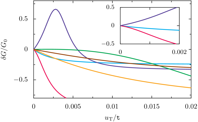
The SGM response for the points and , on the second and third plateaus, depicted by red and purple solid lines in Fig. 5(a), respectively, exhibits an initial quadratic dependence as a function of the potential strength . The corrections are always negative, in agreement with the expectation that the dominant SGM correction at weak tip strength is of second order, and the initial strength dependencies are well described by the perturbative prediction of Eq. (20) (red and purple dash-dotted lines, respectively). It is important to remark that the perturbative regime extends over a relatively large interval and describes rather precisely conductance corrections up to . Moreover, the SGM scan of Fig. 4 confirms the prediction of Eq. (20) of an approximate independence with respect to the tip position, provided that the walls are not approached.
In Fig. 5(b) we present the SGM correction for different potential widths (different symbols) and strengths in a large range (, ), which demonstrates a robust data collapsing. The noninteger power law for the scaling in the variable is consistent with the logarithmic dependence of the function in Eq. (20) for small values of the argument.
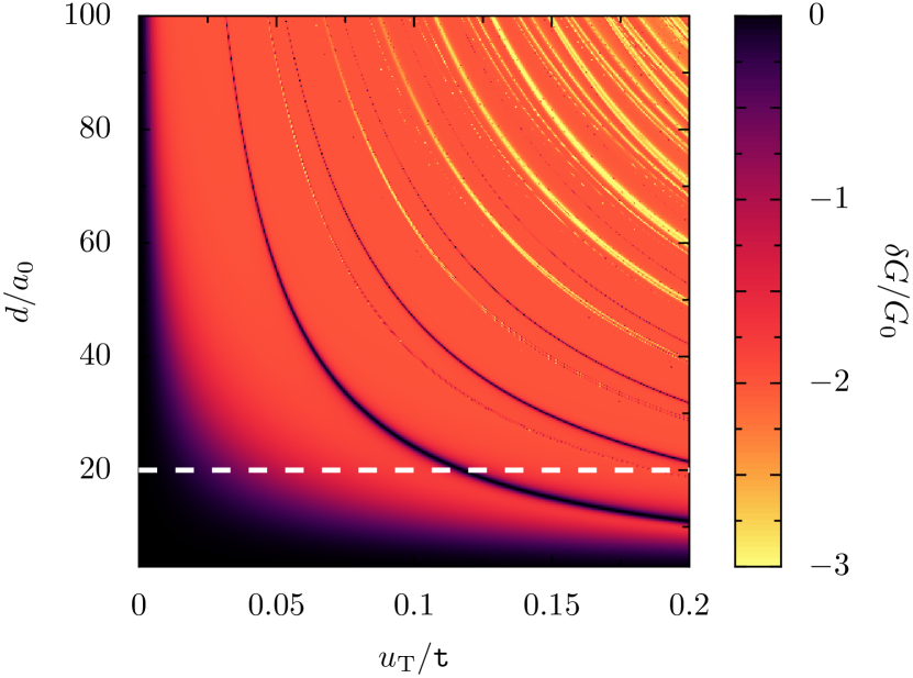
Another remarkable feature of Fig. 5(a) is the revival of the GNR conductance for large values of , outside the perturbative regime. These peaks attain the unitary limit of no conductance correction in the case of the second plateau (red solid line), and can be understood as resonances through states electrostatically confined below the tip in the region defined for sufficiently large values of , like the graphene quantum-dot states studied in Refs. Downing et al. (2011); Schneider and Brouwer (2014). In Fig. 6 the SGM conductance correction is presented in color scale as a function of tip strength and width, highlighting the resonances (dark colors) and antiresonances (light colors) that appear as functions of and when the unperturbed conductance is in the second plateau (point of Fig. 2). These resonance lines indicate the relation between and , under which the confined states under the tip remain aligned with the Fermi energy. The cut shown by the dashed white horizontal line corresponding to indicates the parameters for which the data have been presented in Fig. 5(a) for the second plateau (red solid line), on a slightly larger interval.
The resonances occur at the same tip strengths when the tip position is moved away from the nanoribbon axis. When the edges of the ribbon are approached, the revival occurs at lower tip strength as it can be expected from the behavior of confined states in a truncated potential.
VI SGM correction in a graphene nanoconstriction
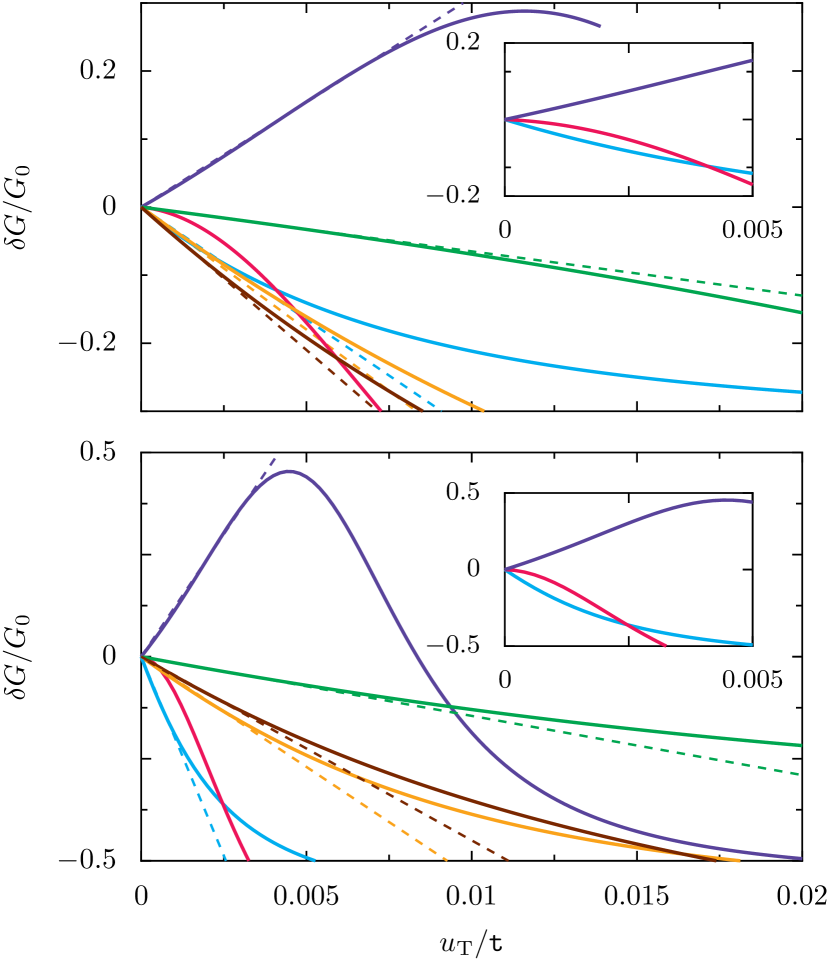
In the case of a GNC defined in a nanoribbon we do not have well-defined conductance plateaus (see colored solid lines in Fig. 2), and therefore, we expect the lowest nonvanishing SGM conductance correction to be the first-order term of Eq. (10), yielding a linear dependence on tip strength in the noninvasive regime. The numerical results of Fig. 7, showing the dependence of the SGM correction as a function of the tip strength for two GNCs shown in Fig. 2 ( and for the upper panel and and for the lower panel) and a tip placed at their center confirm our expectation for all the operating conditions defined in Fig. 3, except for the points and characterizing a maximum of the unperturbed conductance.
Unlike the negative second-order correction that dominates in the conductance plateaus, the first-order correction, indicated by fits of linear dependence (dashed lines with the corresponding color), can be positive or negative. The matrix elements (7) that, together with the unperturbed transmission and reflection amplitudes, determine the value of the conductance correction are more difficult to evaluate than for the case of GNRs, since the scattering wave functions are in general not known (except for particular cases like those of abrupt junctions Wurm et al. (2009)). It can be observed in Fig. 7 that the range of linear behavior is quite reduced, as higher-order terms become relevant already at moderate tip strengths of .
The points and in Fig. 3 (red lines in Fig. 7) correspond to unperturbed unitary transmissions set by the fictitious GNRs of width . The effect of the tip can thus only reduce the conductance, and therefore the second-order correction dominates, resulting in the quadratic dependence for very small values of observed in Fig. 7. Points like and (green lines), corresponding to a plateaulike condition in Fig. 3, exhibit a very small slope, indicating that the linear correction (10) is weakened when approaching the regime of conductance quantization. The overall conductance scale in Fig. 7 of the upper panel is smaller than that of the lower panel, since the former presents the case of a smoother junction than the latter and the well-defined quantized conductance plateaus of the smooth junction weaken the contribution arising from the first-order correction (11).
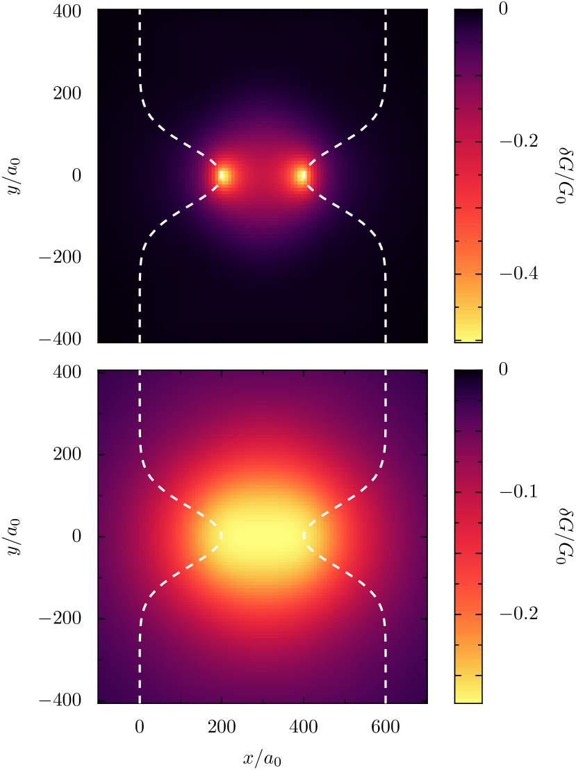
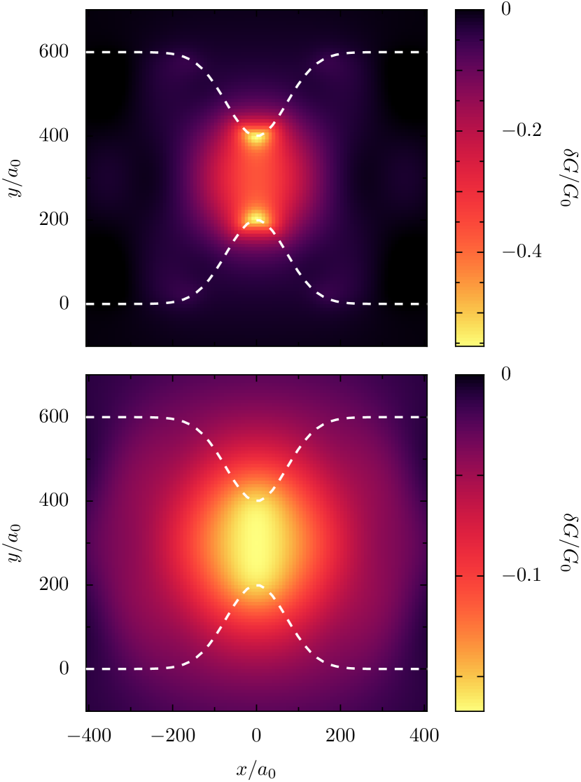
Figure 8 shows the scan of the conductance correction in a GNC, as a function of tip position, with an unperturbed condition corresponding to the point (orange) of Fig. 3(b) for the case of a weak tip in the noninvasive regime () and two values of the tip-potential extent: (upper panel) and (lower panel). In both cases, the strongest SGM response appears when the tip is close to the GNC, in agreement with previous experimental Neubeck et al. (2012) and theoretical work Mreńca et al. (2015); *Mre_ca_Kolasi_ska_2022; Mreńca-Kolasińska and Szafran (2017). Such strong response overwhelms, on the scale of the figures, the modulations seen in Fig. 4 arising from the GNR enclosure. On the one hand, the tip strength is much smaller than that used in the example of SGM in a GNR. On the other hand, the point corresponds to the third plateau of the limiting GNR, described by the point in Fig. 2, where the SGM response is considerably weaker than in the second plateau (point ). The smaller tip () results in a weaker signal than the large tip () since the potential (4) becomes less effective as decreases [see Eq. (41)]. We notice that the SGM conductance correction is not only negative at the center of the constriction [orange line in Fig. 7(b)], but everywhere in the region scanned in Fig. 8.
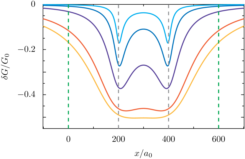
An important difference between the two panels of Fig. 8 is that the SGM response corresponding to the small tip presents a spatial feature with two local minima close to the edges in the narrowest part of the GNC. Figure 9 shows the conductance change when the tip is displaced along the line for different widths (), illustrating how a progressively broader tip blurs the localized features at the edges. The spatial features of Fig. 8 are rather generic, as they appear for most of the unperturbed conditions, but other behavior can be also observed; i.e., for the point (not shown) no concentration of the SGM signal is obtained.
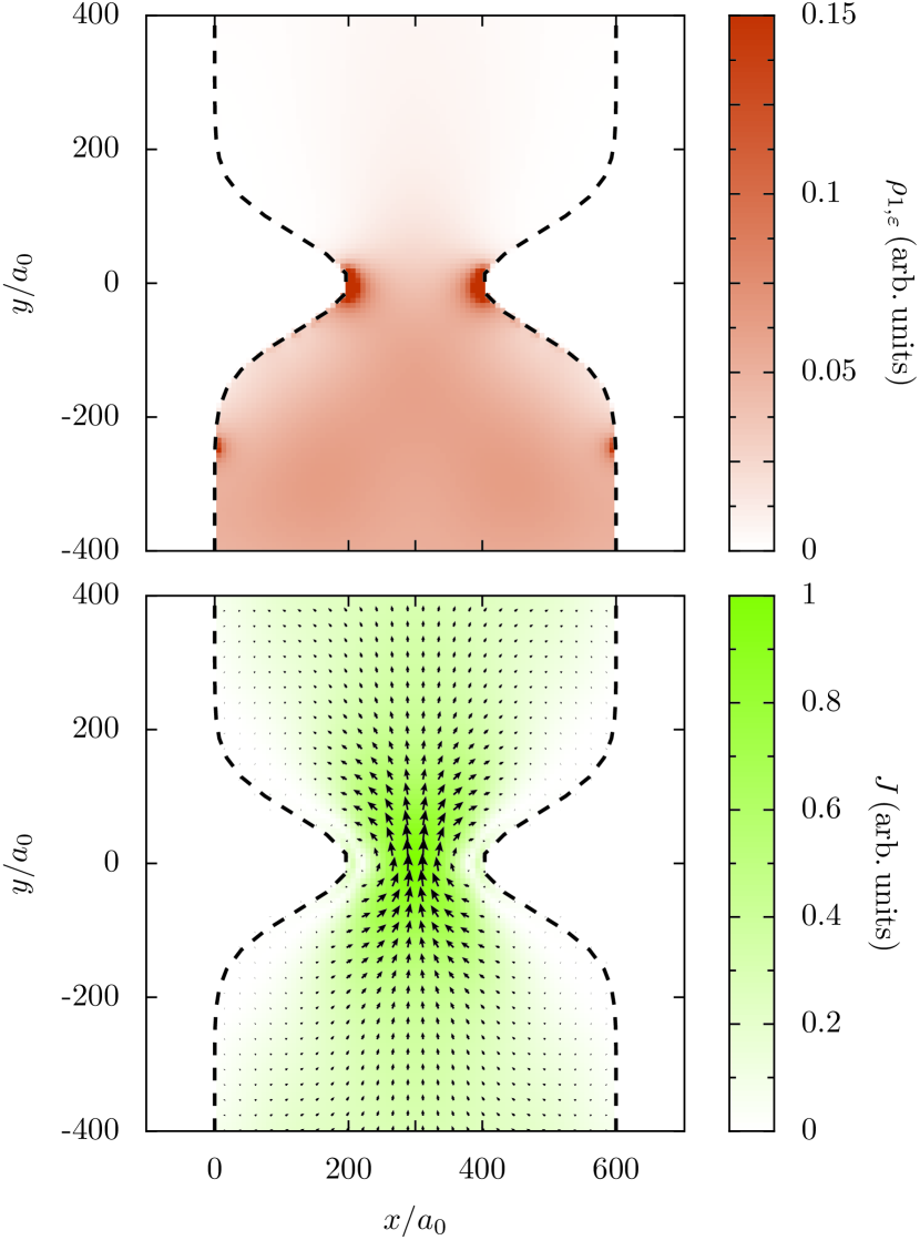
In semiconductor QPCs, it has been shown Ly et al. (2017) that, in certain cases, a weakly invasive SGM response can be connected with the unperturbed partial local density of states (PLDOS), defined as
| (25) |
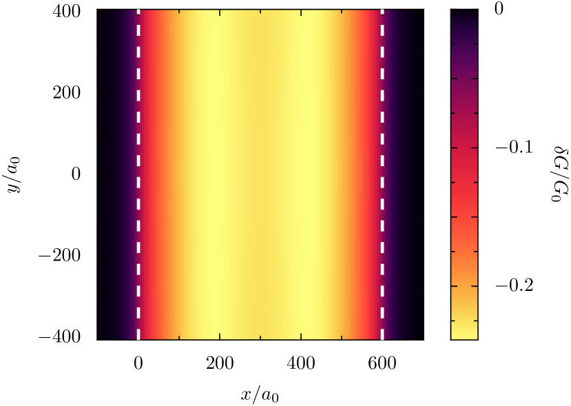
for electrons impinging into the scatterer from lead with an energy , and scattering states given by Eq. (32a). For local tips, there is a linear relationship between the first-order conductance change and the PLDOS in the case of a single open channel, while when the QPC is tuned on a conductance plateau, the second-order conductance correction verifies , when the position of the tip is in the lead where electrons are transmitted. The departures from the above relationship for imperfect transmission were shown to be small, provided the extent of the tip remains small Ly et al. (2017). In the upper panel of Fig. 10, we explore the previous connection and plot the PLDOS of the GNC considered in Fig. 8, obtaining a large enhancement of the PLDOS at the edges in the narrowest part.
An imaging technique using nitrogen-vacancy-center magnetometry has revealed that the current density is concentrated on the edges of the narrowest part of a micrometer-sized constriction operating in the Ohmic regime Jenkins et al. (2022). When lowering the temperature below , the Ohmic regime gives up its place to the ballistic regime and the current density becomes homogeneous along the centerline of the constriction. Our results for the current density (lower panel of Fig. 10) agree with the ballistic ones of Ref. Jenkins et al. (2022). Thus, the strong features appearing in the PLDOS and put in evidence by the SGM response to a relatively small tip do not seem to have an effect on the current density.
VII Zigzag edges
We have so far mainly discussed the case of armchair edges, where the eigenenergies and eigenfunctions have the simple form presented in Appendix A, and analytical expressions could be obtained in the perturbative regime. The case of zigzag edges is more involved since in a GNR the possible transverse quantum numbers depend on the longitudinal momentum. Another difference with respect to the armchair case is the existence in zigzag GNRs of flat bands with small values of , corresponding to chiral eigenstates localized at the edges for each sublattice.
As shown in Fig. 11 the conductance of a zigzag GNR with a width presents a steplike dependence on (thick black solid line). The first conductance plateau at corresponds to the chiral mode in the direction of the current, while the following plateaus are separated by , as a consequence of the mode degeneracy arising from the two graphene valleys.
Once a constriction is defined on a zigzag GNR (with its axis rotated an angle of with respect to the setup of Fig. 1), the resulting conductance is reduced as compared to that of the GNR (thick colored lines in Fig. 11). As remarked in Ref. Ihnatsenka and Kirczenow (2012), the conductance plateaus for zigzag edges are better defined than in the armchair case, especially for the case of a wide GNC. At low energies, the GNC with the largest width (, brown solid line) does not break the perfectly conducting channel of the circumjacent GNR. Narrower GNCs (dark blue, orange, green, and violet solid thick curves) destroy the perfect conducting channel at low energies, where similarly to the case of armchair GNCs of Fig. 2, sharp resonances associated with quasibound states can be observed Xiong and Xiong (2011); Deng et al. (2014). Thin dashed lines represent the conductance of a GNR with a width equal to the narrowest distance of the GNC with the corresponding color. In the zigzag case the conductance of a wide GNC can be larger than the one of the corresponding GNR of width . In Fig. 11 the thick brown and dark blue solid lines may go, in some energy intervals, above the corresponding dashed lines whenever the fictitious GNR has its conductance set at by the perfect conducting channel, while new transverse modes are open in the GNC setup.
The slightly better quality of the conductance plateaus for zigzag edges, as compared with the armchair case, can be understood from the transmission eigenmode decomposition of the conductance. In the former case the modes are turned on as increases (not shown), attaining unitary transmission more sharply than in the case of armchair edges presented in Fig. 3.
The response of an SGM tip for a zigzag GNR presents some similarities and differences with respect to the armchair case. In Fig. 12 we show the numerically obtained SGM corrections as a function of , for a tip with placed on the longitudinal axis of the strip () for three cases where the unperturbed conductance is in the first (blue solid line), second (red solid line), and third (purple solid line) plateau (points , , and of Fig. 11, respectively). Similarly to the case of an armchair GNR presented in Fig. 5(a), the perfectly conducting channel seems to be unaffected by the tip (blue line), while the other two unperturbed conditions exhibit an initial quadratic dependence on followed by a revival of the conductance for larger potential strengths (red and purple lines corresponding to and , respectively). However, this simple picture is modified when the perfect conductance of the chiral modes is destroyed by the effect of the tip.
In Fig. 13 we present the conductance correction as a function of for and the unperturbed conditions defined by the points , , and of Fig. 11 (top, middle, and bottom panels, respectively) when the tip is placed at the center of the strip (same color convention as in Fig. 12), at (brown), and at (green). Remarkable fluctuations appear when the tip approaches the edges, an effect already noticed in the numerical simulations of Ref. Mreńca et al. (2015). Similar features can be observed if the tip is kept on the axis of the strip, while its extent is increased. For the perfect conductance is lost for , and strong oscillations set in afterwards (not shown). These results are consistent with the finding of Ref. Akhmerov et al. (2008) evidencing that, even a smooth potential, if it is strong enough to create a local - junction, leads to considerable scattering in a zigzag GNR, since both valleys are connected by the edge state.
The perturbative approach to the SGM response developed in Sec. IV is difficult to generalize to zigzag edges, due to peculiarities of the GNR spectrum. The existence of flat quasidegenerate bands prevents us from performing the energy integrations as in Eqs. (45) (upon which the perturbative approach is based), since it is not correct to restrict the energy interval of integration to that where belongs. Moreover, the finite size of the zigzag Brillouin zone cannot be represented by the Dirac equation, as this continuous description does not account for the differences that arise according to the parity of the number of atoms across the transverse direction, i.e., the contrast between GNRs having the longitudinal axis of symmetry (zigzag configuration, even ) and without it (antizigzag configuration, odd ) Akhmerov et al. (2008).
The tight-binding model allows one to obtain the form of the edge-state wave functions Zarea and Sandler (2009); Wakabayashi et al. (2010); Wakabayashi and Dutta (2012); Orlof et al. (2013); Talkachov and Babaev (2023), and thus the intervalley tip potential matrix element. Proceeding as in Ref. Akhmerov et al. (2008) by restricting the Hilbert space to the lowest states permits to understand the observed dependence of the SGM response on the tip position or strength, as well as the relevance of the parity of . The dependence on the parity of the number of atoms across the transverse direction appears in the SGM results of zigzag GNRs. The dependence of the conductance correction at different points of the transverse cross section for (not shown) presents qualitative differences with respect to that of shown in Fig. 13. And related departures appear when is varied for two strip widths corresponding to different parities.
The SGM of a GNC defined on a zigzag GNR exhibits similar features as in the case of armchair edges. In Fig. 14 we present the dependence of the conductance correction for a tip with placed at the center of the constriction for the unperturbed conditions defined by the points indicated in Fig. 11. Similarly to the results of Fig. 7, the conductance corrections present an initial dependence which is approximately linear for most of the unperturbed conditions (i.e., points , , , and ), turning into a quadratic one for the conditions corresponding to a conductance maximum (point ) or an approximate conductance plateau (point ).
The SGM scan of Fig. 15 is similar to that of Fig. 8 (up to the rotation). The spatial feature of two local minima close to the edges in the narrowest part of the GNC appearing for small tips (, upper panel), is blurred for larger tip strengths (, lower panel). There are no oscillations of the SGM response close to the edges as in the case of GNRs, since the GNC effectively breaks the perfectly conducting channel.
VIII Conclusions
We have investigated transport in graphene nanoribbons under the influence of the potential of an SGM tip. We have extended the perturbative theory for the SGM response in the regime of noninvasive tips to the case of graphene, and we have demonstrated numerically the validity of the results in the limit of weak tips. On the conductance plateaus observed in metallic armchair ribbons, the tip-induced conductance correction is of second order in the tip strength, and always negative. A particular situation occurs in the zero-transverse-energy mode, where the second-order correction vanishes, leading to nearly perfect transmission. A data collapse appears when the conductance correction is plotted as a particular combination of the tip strength and size, indicating that a small and strong tip leads to the same lowest-order correction as a larger and correspondingly weaker tip.
For the regime of stronger tips, we have found that the conductance contributions from channels above the lowest one exhibit a revival to full transmission at tip strengths that decrease with the tip size. These conductance resonances are interpreted in terms of confined states under the tip potential.
The theory has been applied to constrictions defined in a nanoribbon. In this case, the conductance plateaus are typically lost, and the perturbation approach predicts, for the regime of noninvasive tips, the dominance of a conductance correction that is linear in tip strength. Numerical results confirm such a conclusion, and a quadratic dependence is obtained in the faint surviving plateaus, as well as when the unperturbed condition corresponds to a maximum of the conductance.
Numerical studies of the conductance corrections as a function of tip position yield spatial features when the tip is placed at the narrowest part of the constriction with local maxima close to the edges. Such a behavior is related to a concentration of the unperturbed PLDOS at those points. Nevertheless, the current density does not exhibit a related behavior.
Zigzag nanoribbons present a similar SGM response as in the armchair case, with quadratic conductance corrections, except when the tip potential close to the borders is strong enough to create local - junctions and destroy the perfect conductance of the chiral edge states. A GNC defined on a zigzag nanoribbon typically breaks the perfect channel transmission, and thus the action of the tip is similar to that observed for armchair edges. This result is important, as it is for armchair edges that the perturbative approach for noninvasive tips has been developed, moreover since a GNR with an orientation intermediate between zigzag and armchair has been shown to effectively behave as having zigzag edges Nakada et al. (1996).
Several of the previously mentioned theoretical findings can be experimentally checked in graphene nanostructures, i.e., the initial linear versus quadratic dependence of the SGM correction on the tip-potential strength and its universal scaling, the revival of perfect conductance outside the noninvasive regime, the spatial features of the SGM scans in nanoconstrictions, and the possible destruction of the perfectly conducting channels.
The extension of our theoretical approach to micrometer sizes could allow to analyze the results of Ref. Brun et al. (2019) and make the connection with the semiclassical approaches to electron optics in graphene Cserti et al. (2007); Paredes-Rocha et al. (2021), as well as consider the Ohmic-to-ballistic transition studied in Ref. Jenkins et al. (2022). Moreover, the perturbative expansion developed in our work can be extended to the magnetic field case, in order to address the diversity of field-dependent SGM experiments Morikawa et al. (2015); Bhandari et al. (2016); Bours et al. (2017); Berezovsky and Westervelt (2010); Chuang et al. (2016); Xiang et al. (2016); Moreau et al. (2021); Brun et al. (2020); Moreau et al. . Other possible generalizations of the theory concern bilayer graphene, where SGM has allowed detection of localized states in narrow channels Gold et al. (2020) and the observation of electronic jets emanating from a constriction Gold et al. (2021), as well as transition metal dichalcogenide nanostructures Bhandari et al. (2018); Prokop et al. (2020).
Acknowledgments
We thank Eros Mariani for useful discussions. This work was supported by the National Natural Science Foundation of China under Grant No. 12047501. X.C. acknowledges the financial support from the China Scholarship Council No. 202006180040 and the Programme Doctoral International of the University of Strasbourg.
Appendix A Lead and scattering states for an armchair GNR
In this Appendix we recall the properties of the electronic eigenstates for an armchair nanoribbon and we define the scattering states to be used in the scattering approach for the conductance of a graphene nanostructure connected to semi-infinite leads of the armchair type. Our focus on the armchair case stems from the availability of analytical expressions that can be readily employed in the perturbative treatment of the SGM response.
Instead of using the standard continuous form of the wave functions Brey and Fertig (2006); Tworzydło et al. (2006); Wurm et al. (2009); Bergvall (2014), we adopt a mixed description with a discretization in the direction transverse to the nanoribbon axis, where each lattice point describes a conventional cell. This formulation allows to fix the total number of states participating in the perturbative expansion developed in this work. For an armchair nanoribbon directed along the direction and with unit cells along the transverse direction (see Fig. 1), we take the eigenstate basis
| (26a) | ||||
| (26b) | ||||
with the pseudospinor
| (27) |
for , and . While the actual width of the nanoribbon is , the inclusion of the fictitious sites and where the wave function vanishes (marked as crosses in Fig. 1) translates into an effective width . The quantum numbers characterizing the basis are the energy (), the transverse channel number (limited by the fact that there cannot be more than channels), and the direction () of the longitudinal wave vector (we choose ). In Eq. (26b) we have defined the transverse wave vector and the scaled energy , where . The decomposition (26a) into longitudinal and transverse components is useful for notation purposes and in view of the general relationship Wurm et al. (2011); Carmier et al. (2011)
| (28) |
where is the usual (second) Pauli matrix.
The orthonormality and completeness conditions for the eigenbasis (26) are expressed, respectively, as
| (29a) | |||
| (29b) | |||
where the indices and label the pseudospinor components. Using the relationship (28) we obtain the electrical current per unit energy associated with the state as
| (30) |
Two different cases can be distinguished among armchair nanoribbons, depending on whether or not is a multiple of . The first case is that of metallic nanoribbons with a zero-transverse-energy mode for and , which is nondegenerate, while all the other modes are doubly degenerate [i.e., for we have ]. The second case is that of semiconducting nanoribbons with an energy gap around , and nondegenerate modes everywhere in the spectrum.
The scattering approach to quantum transport in graphene can be developed along similar lines as for the 2DEG of semiconductor-based heterojunctions Jalabert (2016), from the nanoribbon eigenstates (26), by defining the incoming () and outgoing () modes (lead states)
| (31) |
in the semi-infinite leads. We note () for the lower (upper) lead describing (), cf. Fig. 1. The direction of the longitudinal wave vector is defined such that for the up movers ( and ) and for the down movers ( and ). An infinitesimal imaginary part is given to in order to define the proper time ordering, and thus we note (with ).
Once a quantum-coherent scatterer (of linear extension in the direction) is placed at the coordinate origin, the incoming modes give rise to outgoing scattering states, that in the asymptotic regions are given by
| (32a) | |||
| (32b) | |||
The sums are carried over the number of propagating modes , which is the dimension of the matrices () and () characterizing the reflection and transmission amplitudes from lead (). We do not explicitly indicate the energy dependence of the scattering amplitudes.
The outgoing scattering states constitute an eigenbasis. Therefore, the retarded Green function is a matrix admitting the spectral decomposition
| (33) |
with . Taking and we consider
| (34) |
where we have only kept the terms that survive the sums over and . As in Appendix C, we assume that the energy integration is dominated by the values of , and therefore we restrict the integration as to have (and therefore ). The integral can be done by performing the change of variables from to , or to , by using and . Implementing the latter change for the first term of the curly bracket and the former change for the second term, and using Eq. (45), we can write expression (A) as
| (35) |
From definition (31) of the incoming modes and the general relationship (28) for the case , we obtain the Fisher-Lee relation for graphene Wurm et al. (2011); Carmier et al. (2011)
| (36) |
which, together with Eq. (1), gives access to the electron conductance from the knowledge of the Green function, and it is then used in the numerical and analytical approaches of this work.
Appendix B Matrix elements of the tip potential for armchair GNRs
For an armchair GNR, according to definition (7), the matrix element of the tip potential between two scattering states impinging from opposite sides with the same energy can be written as
| (37) |
where we have used that . According to Eqs. (26b) and (27), we have
| (38) |
and
| (39) |
In the case of a metallic GNR, for the zero-transverse-energy mode with and , we immediately see that . Therefore, the matrix element vanishes independently of the strength and the position of the tip, and more generally of the features of the perturbing potential, provided that the latter is long ranged Yamamoto et al. (2009) (and as a consequence it does not induce intervalley scattering).
Leaving aside the trivial case of previously discussed, we readily perform the integral in Eq. (37). Moreover, trading the discrete index by the continuous variable , and noticing that for the lowest-transverse-energy modes the product of the two sines is a rapidly oscillating function of in comparison with the other terms of the integrand, we can write
| (40) |
For , and leaving aside the cases where the distance from the tip to the boundaries is of the order of , we can push the limits of the integration to , obtaining
| (41) |
where is the zeroth-order modified Bessel function of the second kind.
The case of equal-energy scattering states impinging from the same side can be worked out similarly. For we have
| (42) |
As in the previous case, we take into account that the tip potential is smooth on the scale of the lattice constant, we readily perform the integral, and we convert the sum into an integral, obtaining
| (43) |
Performing the integral, we have
| (44) |
Appendix C Energy integrations for the SGM corrections
In this Appendix we work out a few integrations appearing in the perturbative treatment of the tip potential. We first present the results:
| (45a) | ||||
| (45b) | ||||
| (45c) | ||||
| (45d) | ||||
for and , while (with ) are arbitrary functions assumed to have a smooth dependence on and .
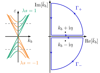
According to definition (31), in the integration of Eq. (45a) we have . The sum over translates into the restriction . Since the energy integration is dominated by the values of , we can restrict the integration as to have (and therefore ). Performing the change of variables from to such that , the left-hand side of Eq. (45a) can be written as
| (46) |
The integral can be done by contour integration in the complex plane. In the case () the contour should be closed on the upper (lower) half plane with positive (negative) values of in order to have vanishing contributions from the vertical and quarter-circle segments for large values of (see Fig. 16). Such contours leave aside the other poles at , as well as the branch cuts associated with the square root. Therefore, the contour integral is determined by the pole at , and we readily recover the result (45a). The integral of Eq. (45b), where we also have , follows along the same lines of the previous case.
In the integrand of Eq. (45c) we have and the sum over leads to the condition . Restricting the interval of the energy integration such that (and therefore ) and performing the same change of variables specified above, the left-hand side of Eq. (45c) can be written as
| (47) |
For the case () the contour should be closed on the lower (upper) half plane with negative (positive) values of in order to have vanishing contributions from the vertical and quarter-circle segments (see Fig. 16), and the absence of poles inside the contour results in a vanishing integral, as stated in Eq. (45c). The integral of Eq. (45d), where we also have , follows along the same lines of the previous case.
We continue with the demonstration of an important identity concerning the zero-transverse-energy mode of the metallic armchair GNR:
| (48) |
Concentrating on the -dependent terms of the integrand above, we need to evaluate
| (49) |
We note and . The above integral can be readily done by contour integral in the complex plane, and thus
| (50) |
where is the Heaviside step function. Since the only dependence of the integrand is that of , it is easy to see that the integrals can be taken as unrestricted, trading by a factor of . Therefore, Eq. (C) can be expressed as the product of two matrix elements of the tip potential, and we recover the result (48), implying that the principal part of the integral vanishes.
The result (48) can be generalized to the case of intermediate energy integrations, leading to
| (51) |
Such a result can be obtained by expressing the matrix elements in terms of the corresponding wave functions, and then performing the energy integrations independently, which yields a factor of and the constraint . As before, the only dependence of the integrand is contained in the tip potentials , and therefore the integral can be taken as unrestricted by trading the Heaviside step function by a factor of , which results in the matrix element to the th power.
References
- Novoselov et al. (2004) K. S. Novoselov, A. K. Geim, S. V. Morozov, D. Jiang, Y. Zhang, S. V. Dubonos, I. V. Grigorieva, and A. A. Firsov, “Electric field effect in atomically thin carbon films,” Science 306, 666 (2004).
- Novoselov et al. (2005) K. S. Novoselov, A. K. Geim, S. V. Morozov, D. Jiang, M. I. Katsnelson, I. V. Grigorieva, S. V. Dubonos, and P. Kim, “Two-dimensional gas of massless Dirac fermions in graphene,” Nature (London) 438, 197 (2005).
- Castro Neto et al. (2009) A. H. Castro Neto, F. Guinea, N. M. R. Peres, K. S. Novoselov, and A. K. Geim, “The electronic properties of graphene,” Rev. Mod. Phys. 81, 109 (2009).
- Peres (2010) N. M. R. Peres, “Colloquium: The transport properties of graphene: An introduction,” Rev. Mod. Phys. 82, 2673–2700 (2010).
- Topinka et al. (2000) M. A. Topinka, B. J. LeRoy, S. E. J. Shaw, E. J. Heller, R. M. Westervelt, K. D. Maranowski, and A. C. Gossard, “Imaging coherent electron flow from a quantum point contact,” Science 289, 2323 (2000).
- Sellier et al. (2011) H. Sellier, B. Hackens, M. G. Pala, F. Martins, S. Baltazar, X. Wallart, L. Desplanque, V. Bayot, and S. Huant, “On the imaging of electron transport in semiconductor quantum structures by scanning-gate microscopy: successes and limitations,” Semicond. Sci. Technol. 26, 064008 (2011).
- Schnez et al. (2010) S. Schnez, J. Güttinger, M. Huefner, C. Stampfer, K. Ensslin, and T. Ihn, “Imaging localized states in graphene nanostructures,” Phys. Rev. B 82, 165445 (2010).
- Pascher et al. (2012) N. Pascher, D. Bischoff, T. Ihn, and K. Ensslin, “Scanning gate microscopy on a graphene nanoribbon,” Appl. Phys. Lett. 101, 063101 (2012).
- Garcia et al. (2013) A. G. F. Garcia, M. König, D. Goldhaber-Gordon, and K. Todd, “Scanning gate microscopy of localized states in wide graphene constrictions,” Phys. Rev. B 87, 085446 (2013).
- Jalilian et al. (2011) R. Jalilian, L. A. Jauregui, G. Lopez, J. Tian, C. Roecker, M. M. Yazdanpanah, R. W. Cohn, I. Jovanovic, and Y. P. Chen, “Scanning gate microscopy on graphene: charge inhomogeneity and extrinsic doping,” Nanotechnology 22, 295705 (2011).
- Morikawa et al. (2015) S. Morikawa, Z. Dou, S.-W. Wang, C. G. Smith, K. Watanabe, T. Taniguchi, S. Masubuchi, T. Machida, and M. R. Connolly, “Imaging ballistic carrier trajectories in graphene using scanning gate microscopy,” Appl. Phys. Lett. 107, 243102 (2015).
- Bhandari et al. (2016) S. Bhandari, G.-H. Lee, A. Klales, K. Watanabe, T. Taniguchi, E. Heller, P. Kim, and R. M. Westervelt, “Imaging cyclotron orbits of electrons in graphene,” Nano Lett. 16, 1690 (2016).
- Cabosart et al. (2017) D. Cabosart, A. Felten, N. Reckinger, A. Iordanescu, S. Toussaint, S. Faniel, and B. Hackens, “Recurrent quantum scars in a mesoscopic graphene ring,” Nano Lett. 17, 1344 (2017).
- Berezovsky et al. (2010) J. Berezovsky, M. F. Borunda, E. J. Heller, and R. M. Westervelt, “Imaging coherent transport in graphene (part I): mapping universal conductance fluctuations,” Nanotechnology 21, 274013 (2010).
- Berezovsky and Westervelt (2010) J. Berezovsky and R. M. Westervelt, “Imaging coherent transport in graphene (part II): probing weak localization,” Nanotechnology 21, 274014 (2010).
- Chuang et al. (2016) C. Chuang, M. Matsunaga, F.-H. Liu, T.-P. Woo, N. Aoki, L.-H. Lin, B.-Y. Wu, Y. Ochiai, and C.-T. Liang, “Probing weak localization in chemical vapor deposition graphene wide constriction using scanning gate microscopy,” Nanotechnology 27, 075601 (2016).
- Neubeck et al. (2012) S. Neubeck, L. A. Ponomarenko, A. S. Mayorov, S. V. Morozov, R. Yang, and K. S. Novoselov, “Scanning gate microscopy on a graphene quantum point contact,” Physica E 44, 1002 (2012).
- Brun et al. (2019) B. Brun, N. Moreau, S. Somanchi, V.-H. Nguyen, K. Watanabe, T. Taniguchi, J.-C. Charlier, C. Stampfer, and B. Hackens, “Imaging Dirac fermions flow through a circular Veselago lens,” Phys. Rev. B 100, 041401(R) (2019).
- Guerra (2021) M. Guerra, “Electron optics in ballistic graphene studied by scanning gate microscopy,” PhD thesis, Université Grenoble Alpes (2021).
- Xiang et al. (2016) S. Xiang, A. Mreńca-Kolasińska, V. Miseikis, S. Guiducci, K. Kolasiński, C. Coletti, B. Szafran, F. Beltram, S. Roddaro, and S. Heun, “Interedge backscattering in buried split-gate-defined graphene quantum point contacts,” Phys. Rev. B 94, 155446 (2016).
- Bours et al. (2017) L. Bours, S. Guiducci, A. Mreńca-Kolasińska, B. Szafran, J. C. Maan, and S. Heun, “Manipulating quantum Hall edge channels in graphene through scanning gate microscopy,” Phys. Rev. B 96, 195423 (2017).
- Moreau et al. (2021) N. Moreau, B. Brun, S. Somanchi, K. Watanabe, T. Taniguchi, C. Stampfer, and B. Hackens, “Upstream modes and antidots poison graphene quantum hall effect,” Nat. Commun. 12, 4265 (2021).
- Moreau (2022) N. Moreau, “Scanning gate imaging and tuning of quantum electronic transport in graphene,” PhD thesis, UCL - Ecole Polytechnique de Louvain (2022).
- Petrović et al. (2017) M. D. Petrović, S. P. Milovanović, and F. M. Peeters, “Scanning gate microscopy of magnetic focusing in graphene devices: quantum versus classical simulation,” Nanotechnology 28, 185202 (2017).
- Mreńca et al. (2015) A. Mreńca, K. Kolasiński, and B. Szafran, “Conductance response of graphene nanoribbons and quantum point contacts in scanning gate measurements,” Semicond. Sci. Tech. 30, 085003 (2015).
- Mre (2022) “Corrigendum,” Semicond. Sci. Tech. 37, 049501 (2022).
- Mreńca-Kolasińska and Szafran (2017) A. Mreńca-Kolasińska and B. Szafran, “Imaging backscattering in graphene quantum point contacts,” Phys. Rev. B 96, 165310 (2017).
- Jalabert et al. (2010) R. A. Jalabert, W. Szewc, S. Tomsovic, and D. Weinmann, “What is measured in the scanning gate microscopy of a quantum point contact?” Phys. Rev. Lett. 105, 166802 (2010).
- Gorini et al. (2013) C. Gorini, R. A. Jalabert, W. Szewc, S. Tomsovic, and D. Weinmann, “Theory of scanning gate microscopy,” Phys. Rev. B 88, 035406 (2013).
- Groth et al. (2014) C. W. Groth, M. Wimmer, A. R. Akhmerov, and X. Waintal, “Kwant: a software package for quantum transport,” New J. Phys. 16, 063065 (2014).
- Lin et al. (2008) Y.-M. Lin, V. Perebeinos, Z. Chen, and P. Avouris, “Electrical observation of subband formation in graphene nanoribbons,” Phys. Rev. B 78, 161409(R) (2008).
- Jiao et al. (2009) L. Jiao, L. Zhang, X. Wang, G. Diankov, and H. Dai, “Narrow graphene nanoribbons from carbon nanotubes,” Nature (London) 458, 877 (2009).
- Lian et al. (2010) C. Lian, K. Tahy, T. Fang, G. Li, H.G. Xing, and D. Jenaa, “Quantum transport in graphene nanoribbons patterned by metal masks,” Appl. Phys. Lett. 96, 103109 (2010).
- Cai et al. (2010) J. Cai, P. Ruffieux, R. Jaafar, M. Bieri, T. Braun, S. Blankenburg, M. Muoth, A. P. Seitsonen, M. Saleh, X. Feng, K Müllen, and R. Fasel, “Atomically precise bottom-up fabrication of graphene nanoribbons,” Nature (London) 466, 470 (2010).
- Baringhaus et al. (2014) J. Baringhaus, M. Ruan, F. Edler, A. Tejeda, M. Sicot, A. Taleb-Ibrahimi, A.-P. Li, Z. Jiang, E. H. Conrad, C. Berger, C. Tegenkamp, and W. A. de Heer, “Exceptional ballistic transport in epitaxial graphene nanoribbons,” Nature (London) 506, 349 (2014).
- Rizzo et al. (2020) D. J. Rizzo, G. Veber, J. Jiang, R. McCurdy, T. Cao, C. Bronner, T. Chen, S. G. Louie, F. R. Fischer, and M. F. Crommie, “Inducing metallicity in graphene nanoribbons via zero-mode superlattices,” Science 369, 1597 (2020).
- Nakada et al. (1996) K. Nakada, M. Fujita, G. Dresselhaus, and M. S. Dresselhaus, “Edge state in graphene ribbons: Nanometer size effect and edge shape dependence,” Phys. Rev. B 54, 17954 (1996).
- Brey and Fertig (2006) L. Brey and H. A. Fertig, “Electronic states of graphene nanoribbons studied with the Dirac equation,” Phys. Rev. B 73, 235411 (2006).
- Wurm et al. (2009) J. Wurm, M. Wimmer, İ. Adagideli, K. Richter, and H. U. Baranger, “Interfaces within graphene nanoribbons,” New J. Phys. 11, 095022 (2009).
- Yamamoto et al. (2009) M. Yamamoto, Y. Takane, and K. Wakabayashi, “Nearly perfect single-channel conduction in disordered armchair nanoribbons,” Phys. Rev. B 79, 125421 (2009).
- Wakabayashi et al. (2010) K. Wakabayashi, K. Sasaki, T. Nakanishi, and T. Enoki, “Electronic states of graphene nanoribbons and analytical solutions,” Sci. Technol. Adv. Mat. 11, 054504 (2010).
- Wurm et al. (2012) J. Wurm, M. Wimmer, and K. Richter, “Symmetries and the conductance of graphene nanoribbons with long-range disorder,” Phys. Rev. B 85, 245418 (2012).
- Bergvall (2014) A. Bergvall, “Quantum transport theory in graphene,” PhD thesis, Chalmers University of Technology (2014).
- Cao et al. (2017) T. Cao, F. Zhao, and S. G. Louie, “Topological phases in graphene nanoribbons: Junction states, spin centers, and quantum spin chains,” Phys. Rev. Lett. 119, 076401 (2017).
- Muñoz Rojas et al. (2006) F. Muñoz Rojas, D. Jacob, J. Fernández-Rossier, and J. J. Palacios, “Coherent transport in graphene nanoconstrictions,” Phys. Rev. B 74, 195417 (2006).
- Li and Lu (2008) T. C. Li and S.-P. Lu, “Quantum conductance of graphene nanoribbons with edge defects,” Phys. Rev. B 77, 085408 (2008).
- Mucciolo et al. (2009) E. R. Mucciolo, A. H. Castro Neto, and C. H. Lewenkopf, “Conductance quantization and transport gaps in disordered graphene nanoribbons,” Phys. Rev. B 79, 075407 (2009).
- Ihnatsenka and Kirczenow (2009) S. Ihnatsenka and G. Kirczenow, “Conductance quantization in strongly disordered graphene ribbons,” Phys. Rev. B 80, 201407(R) (2009).
- Orlof et al. (2013) A. Orlof, J. Ruseckas, and I. V. Zozoulenko, “Effect of zigzag and armchair edges on the electronic transport in single-layer and bilayer graphene nanoribbons with defects,” Phys. Rev. B 88, 125409 (2013).
- Ruffieux et al. (2016) P. Ruffieux, S. Wang, B. Yang, C. Sánchez-Sánchez, J. Liu, T. Dienel, L. Talirz, P. Shinde, C. A. Pignedoli, D. Passerone, T. Dumslaff, X. Feng, K. Müllen, and R. Fasel, “On-surface synthesis of graphene nanoribbons with zigzag edge topology,” Nature (London) 531, 489 (2016).
- Kolmer et al. (2020) M. Kolmer, A.-K. Steiner, I. Izydorczyk, W. Ko, M. Engelund, M. Szymonski, A.-P. Li, and K. Amsharov, “Rational synthesis of atomically precise graphene nanoribbons directly on metal oxide surfaces,” Science 369, 571 (2020).
- Wang et al. (2021) H. Wang, H. S. Wang, C. Ma, L. Chen, C. Jiang, C. Chen, X. Xie, A.-P. Li, and X. Wang, “Graphene nanoribbons for quantum electronics,” Nat. Rev. Phys. 3, 791 (2021).
- van Wees et al. (1988) B. J. van Wees, H. van Houten, C. W. J. Beenakker, J. G. Williamson, L. P. Kouwenhoven, D. van der Marel, and C. T. Foxon, “Quantized conductance of point contacts in a two-dimensional electron gas,” Phys. Rev. Lett. 60, 848 (1988).
- Wharam et al. (1988) D. A. Wharam, T. J. Thornton, R. Newbury, M. Pepper, H. Ahmed, J. E. F. Frost, D. G. Hasko, D. C. Peacock, D. A. Ritchie, and G. A. C. Jones, “One-dimensional transport and the quantisation of the ballistic resistance,” J. Phys. C: Solid State Phys. 21, L209 (1988).
- Tombros et al. (2011) N. Tombros, A. Veligura, J. Junesch, M. H. D. Guimarães, I. J. Vera-Marun, H. T. Jonkman, and B. J. van Wees, “Quantized conductance of a suspended graphene nanoconstriction,” Nat. Phys. 7, 697 (2011).
- Terrés et al. (2016) B. Terrés, L. A. Chizhova, F. Libisch, J. Peiro, D. Jörger, S. Engels, A. Girschik, K. Watanabe, T. Taniguchi, S. V. Rotkin, J. Burgdörfer, and C. Stampfer, “Size quantization of Dirac fermions in graphene constrictions,” Nat. Commun. 7, 11528 (2016).
- Kinikar et al. (2017) A. Kinikar, T. Phanindra Sai, S. Bhattacharyya, A. Agarwala, T. Biswas, S. K. Sarker, H. R. Krishnamurthy, M. Jain, V. B. Shenoy, and A. Ghosh, “Quantized edge modes in atomic-scale point contacts in graphene,” Nat. Nanotechnol. 12, 564 (2017).
- Kun et al. (2020) P. Kun, B. Fülöp, G. Dobrik, P. Nemes-Incze, I. E. Lukács, S. Csonka, C. Hwang, and L. Tapasztó, “Robust quantum point contact operation of narrow graphene constrictions patterned by AFM cleavage lithography,” npj 2D Mater. Appl. 4, 43 (2020).
- Clericò et al. (2018) V. Clericò, J. A. Delgado-Notario, M. Saiz-Bretín, C. Hernández Fuentevilla, A. V. Malyshev, J. D. Lejarreta, E. Diez, and F. Domínguez-Adame, “Quantized electron transport through graphene nanoconstrictions,” Phys. Status Solidi A 215, 1701065 (2018).
- Glazman et al. (1988) L. I. Glazman, G. B. Lesovik, D. E. Khmel’nitskii, and R. I. Shekter, “Reflectionless quantum transport and fundamental ballistic-resistance steps in microscopic constrictions,” Pis’ma Zh. Eksp. Teor. Fiz. 48, 218 (1988).
- gla (1988) JETP Lett. 48, 238 (1988).
- Szafer and Stone (1989) A. Szafer and A. D. Stone, “Theory of quantum conduction through a constriction,” Phys. Rev. Lett. 62, 300 (1989).
- Katsnelson (2007) M. I. Katsnelson, “Conductance quantization in graphene nanoribbons: adiabatic approximation,” Eur. Phys. J. B 57, 225 (2007).
- Ihnatsenka and Kirczenow (2012) S. Ihnatsenka and G. Kirczenow, “Conductance quantization in graphene nanoconstrictions with mesoscopically smooth but atomically stepped boundaries,” Phys. Rev. B 85, 121407(R) (2012).
- Yannouleas et al. (2015) C. Yannouleas, I. Romanovsky, and U. Landman, “Interplay of relativistic and nonrelativistic transport in atomically precise segmented graphene nanoribbons,” Sci. Rep. 5, 7893 (2015).
- Guimarães et al. (2012) M. H. D. Guimarães, O. Shevtsov, X. Waintal, and B. J. van Wees, “From quantum confinement to quantum Hall effect in graphene nanostructures,” Phys. Rev. B 85, 075424 (2012).
- Xiong and Xiong (2011) Y.-J. Xiong and B.-K. Xiong, “Resonant transport through graphene nanoribbon quantum dots,” J. Appl. Phys. 109, 103707 (2011).
- Deng et al. (2014) Hai-Yao Deng, Katsunori Wakabayashi, and Chi-Hang Lam, “Formation mechanism of bound states in graphene point contacts,” Phys. Rev. B 89, 045423 (2014).
- Jalabert (2016) R. A. Jalabert, “Mesoscopic transport and quantum chaos,” Scholarpedia 11, 30946 (2016).
- Brun et al. (2020) B. Brun, N. Moreau, S. Somanchi, V.-H. Nguyen, A. Mreńca-Kolasińska, K. Watanabe, T. Taniguchi, J.-C. Charlier, C. Stampfer, and B. Hackens, “Optimizing Dirac fermions quasi-confinement by potential smoothness engineering,” 2D Mater. 7, 025037 (2020).
- Downing et al. (2011) C. A. Downing, D. A. Stone, and M. E. Portnoi, “Zero-energy states in graphene quantum dots and rings,” Phys. Rev. B 84, 155437 (2011).
- Schneider and Brouwer (2014) M. Schneider and P. W. Brouwer, “Density of states as a probe of electrostatic confinement in graphene,” Phys. Rev. B 89, 205437 (2014).
- Ly et al. (2017) O. Ly, R. A. Jalabert, S. Tomsovic, and D. Weinmann, “Partial local density of states from scanning gate microscopy,” Phys. Rev. B 96, 125439 (2017).
- Jenkins et al. (2022) A. Jenkins, S. Baumann, H. Zhou, S. A. Meynell, Y. Daipeng, K. Watanabe, T. Taniguchi, A. Lucas, A. F. Young, and A. C. Bleszynski Jayich, “Imaging the breakdown of Ohmic transport in graphene,” Phys. Rev. Lett. 129, 087701 (2022).
- Akhmerov et al. (2008) A. R. Akhmerov, J. H. Bardarson, A. Rycerz, and C. W. J. Beenakker, “Theory of the valley-valve effect in graphene nanoribbons,” Phys. Rev. B 77, 205416 (2008).
- Zarea and Sandler (2009) M. Zarea and N. Sandler, “Graphene zigzag ribbons, square lattice models and quantum spin chains,” New J. Phys. 11, 095014 (2009).
- Wakabayashi and Dutta (2012) K. Wakabayashi and S. Dutta, “Nanoscale and edge effect on electronic properties of graphene,” Solid State Commun. 152, 1420 (2012).
- Talkachov and Babaev (2023) A. Talkachov and E. Babaev, “Wave functions and edge states in rectangular honeycomb lattices revisited: Nanoflakes, armchair and zigzag nanoribbons, and nanotubes,” Phys. Rev. B 107, 045419 (2023).
- Cserti et al. (2007) J. Cserti, A. Pályi, and C. Péterfalvi, “Caustics due to a negative refractive index in circular graphene - junctions,” Phys. Rev. Lett. 99, 246801 (2007).
- Paredes-Rocha et al. (2021) E. Paredes-Rocha, Y. Betancur-Ocampo, N. Szpak, and T. Stegmann, “Gradient-index electron optics in graphene - junctions,” Phys. Rev. B 103, 045404 (2021).
- (81) N. Moreau, B. Brun, S. Somanchi, K. Watanabe, T. Taniguchi, C. Stampfer, and B. Hackens, “Quantum Hall nano-interferometer in graphene,” arXiv:2110.07979 .
- Gold et al. (2020) C. Gold, A. Kurzmann, K. Watanabe, T. Taniguchi, K. Ensslin, and T. Ihn, “Scanning gate microscopy of localized states in a gate-defined bilayer graphene channel,” Phys. Rev. Research 2, 043380 (2020).
- Gold et al. (2021) C. Gold, A. Knothe, A. Kurzmann, A. Garcia-Ruiz, K. Watanabe, T. Taniguchi, V. Fal’ko, K. Ensslin, and T. Ihn, “Coherent jetting from a gate-defined channel in bilayer graphene,” Phys. Rev. Lett. 127, 046801 (2021).
- Bhandari et al. (2018) S. Bhandari, K. Wang, K. Watanabe, T. Taniguchi, P. Kim, and R. M. Westervelt, “Imaging quantum dot formation in MoS2 nanostructures,” Nanotechnology 29, 42LT03 (2018).
- Prokop et al. (2020) M. Prokop, D. Gut, and M. P. Nowak, “Scanning gate microscopy mapping of edge current and branched electron flow in a transition metal dichalcogenide nanoribbon and quantum point contact,” J. Phys.: Condens. Matter 32, 205302 (2020).
- Tworzydło et al. (2006) J. Tworzydło, B. Trauzettel, M. Titov, A. Rycerz, and C. W. J. Beenakker, “Sub-Poissonian shot noise in graphene,” Phys. Rev. Lett. 96, 246802 (2006).
- Wurm et al. (2011) J. Wurm, K. Richter, and İ. Adagideli, “Edge effects in graphene nanostructures: Semiclassical theory of spectral fluctuations and quantum transport,” Phys. Rev. B 84, 205421 (2011).
- Carmier et al. (2011) P. Carmier, C. Lewenkopf, and D. Ullmo, “Semiclassical magnetotransport in graphene - junctions,” Phys. Rev. B 84, 195428 (2011).