High-frequency diode effect in superconducting Nb3Sn micro-bridges
Abstract
The superconducting diode effect has been recently reported in a variety of systems and different symmetry breaking mechanisms have been examined. However, the frequency range of these potentially important devices still remains obscure. We investigated superconducting micro-bridges of Nb3Sn in out-of-plane magnetic fields; optimum magnetic fields of 10 mT generate 10% diode efficiency, while higher fields of 15-20 mT quench the effect. The diode changes its polarity with magnetic field reversal. We documented superconductive diode rectification at frequencies up to 100 kHz, the highest reported as of today. Interestingly, the bridge resistance during diode operation reaches a value that is a factor of two smaller than in its normal state, which is compatible with the vortex-caused mechanism of resistivity. This is confirmed by finite element modeling based on time-dependent Ginzburg-Landau equations. To explain experimental findings, no assumption of lattice thermal inequilibrium was required. Dissimilar edges of the superconductor strip can be responsible for the inversion symmetry breaking by vortex penetration barrier; visual evidence of this opportunity was revealed by scanning electron microscopy. Estimates are in favor of much higher (GHz) range of frequencies for this type of diode.
I Introduction
For certain important problems of fundamental physics, such as the exploration of possible quasi-local action of curl-less vector potential [1], it is necessary to explore superconducting micro-bridges for assurance that the magnitudes of critical currents of the bridge are equal for both current polarities. In particular, accidental breaking of time reversal symmetry (TRS) by remanent or spurious magnetic fields in the cryostat together with simultaneous inversion symmetry (IS) breaking by, e.g., physical asymmetry of the bridge edges can cause the superconducting diode effect (SDE) which violates this equality [2, 3, 4, 5, 6, 7, 8, 9]. While this equality violation should be avoided for the above-mentioned task, it is underlying for the SDE.
Recently, the SDE attracted noticeable attention within the research community [10, 3, 4, 2, 6, 5, 11, 9, 8, 7, 12, 13, 14, 15, 16, 17, 18, 19, 20, 21, 22], and the related activity generated multiple mechanisms applicable to understanding the SDE. In theoretical models, the TRS is broken by an externally applied magnetic field or internal inclusions of magnetic micro-clusters, while the IS is broken by the out-of-plane Rashba spin–orbit coupling [14, 17, 19, 18, 15], valley-Zeeman interaction [13], etc., which results in the emergence of a chiral superconducting order [14, 17, 19, 15]. Experimentally, systems based on van der Waals material with noncentrosymmetric crystal potential [10], synthetic super lattice of [5], and intrinsically IS broken NbSe2 [11] have been reported as well as planar Josephson junction arrays of on [7, 12]. Yet other systems reveal nonreciprocal behavior in field-free environments, such as -based Josephson junction [8], tri-layer graphene [16], and Josephson junction based on chiral superconductor Sr2RuO4 with the internally broken TRS [20]. In view of a variety of experimental observations and theories on the SDE in systems of different configuration, it is quite reasonable to assume that more than one mechanism can be responsible for the ubiquity of nonreciprocity observations in superconductor thin films [23]. In a recent article [24], the SDE was found in micro-bridges in an out-of-plane magnetic field. This observation was attributed to the critical current being determined by the vortex flow, confirming that the SDE is caused by unequal vortex barriers on the two edges of the bridge [25, 26].
To understand this mechanism, consider a type-II superconductor film strip. A magnetic field above a certain critical value creates vortices; initially, they nucleate at the strip edges [27, 28]. Morphology of these edges affects the surface barrier, which prevents the vortices from entering into the strip [29, 30]. However, if the current through the strip is strong enough, the Lorentz force which it exerts onto the vortices overcomes the surface barrier; vortices start moving across the strip, thus dissipating energy and creating a resistive state. In practice, vortex barriers are unequal because of the non-identical structure of strip edges. This circumstance was used by Vodolazov and Peeters [26] when predicting the SDE in 2005. It was experimentally observed recently [24].
The spike of activities in the area of superconducting diodes paves the way towards future practical application of these novel devices in superconducting electronics. However, a very important topic is still open and remains mainly unaddressed: the frequency range of the SDE. In the report by Lyu et al. [31] experiments have been performed at 30 kHz; however, the diode outputs were acquired by a DC nanovoltmeter, which leaves the dynamics of device obscure. Here, we directly detect the voltage response in the time domain at frequencies up to 100 kHz. Experimental findings and modeling results provided us grounds to conclude that the SDE can perform at much higher frequencies.
II Experimental details
Our study used conventional superconducting thin film bridges. The films were prepared in a DC/RF magnetron sputtering system (manufactured by AJA International, Inc.) with a base pressure of Torr. The target (Kurt Lesker, ) was placed inside a DC gun while the target (Kurt Lesker, ) was sputtered using an RF source to avoid melting. The sapphire substrate (AdValue Technology, thickness µm, -cut) was cleaned thoroughly with isopropyl alcohol before it was mounted on the holder. In our chamber’s configuration, the substrate holder is at the center of the chamber facing upwards, while the (five) sputtering guns are located at the top. The substrate is rotated in-plane throughout the whole deposition process to ensure homogeneous deposition layer over the whole surface. Our pre-deposition in-situ cleaning of the substrate involves heating it up to 900°C for 10 min followed by a gentle bombardment of ions at 400°C for 5 min. The substrate was oriented to face the ion gun squarely. For the film deposition, we used a “stack+anneal” process similar to the one in [32]. Taking advantage of the Nb-Sn phase diagram [33], an alternating and stacks with an excess content (Nb:Sn ratio ) “phase-locks” into the composition when the excess Sn evaporates during post-deposition annealing. For the first/base layer, was sputtered in DC mode with 500 W power and 3 mTorr pressure at 600°C for 20 min. Then, the Sn layer was deposited on top of in RF mode with 250 W power and 30 mTorr pressure at 100°C for 15 min. Nb was deposited one more time as the capping (third) layer using the same parameters as the base layer for 3 min. Finally, the substrate was heated in-situ to 950°C for 30 minutes to let the excess Sn evaporate before cooling down to room temperature. All the heating/cooling protocols consistently used a 30°C/min ramp rate. Our films are nm thick and resistivity measurements in PPMS (Quantum Design) indicated the correct Nb3Sn stoichiometry and homogeneity in view of their consistently measured K and RRR(K/K) between samples across several batches, which was corroborated by VSM measurements. Lastly, the stoichiometry was also checked by the SEM EDX (Hitachi SU3500, Oxford Instruments X-MAX-20).
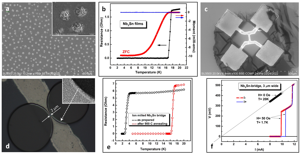
Figure 1 demonstrates certain physical properties of our films (panels a and b) and bridges (panels c-f).
Transformation of the films into bridges was performed using a combination of 3D-printing (Elegoo Mars-3 printer), photolithography and ion milling to achieve macroscopic contact pads on cm2 sapphire substrates. Reactive ion milling (Bal-Tec RES-101, etchant) was used to develop a metallic film pattern, Fig. 1(c). After removal of the resin, the structure was covered by negative photoresist (PKP-308PI, Transene Co., Inc.), and the 100 µm-scale bridge was narrowed down to 12 µm with the projective photolithography (using mask projection via LUMAM epi-fluorescent microscope, objective). After ion milling, the last stage of patterning was undertaken using positive photoresist (TRANSIST PC800, Transene Co., Inc.) and the same projective technique with the objective and a different mask in the form of two holes. The final ion milling delivered bridges about 10-20 µm long and down to 2 µm wide, Fig. 1(d).
Ion milling affects the physical properties of bridges thus reducing the critical temperatures down to the 2-12 K range. This -reduction was also noticed in the literature [24]. We were able to restore the values up to 17 K in some of the bridges by high-vacuum post-annealing ( Torr) at 900°C for 30 min, as shown in Fig. 1(e).
III Results
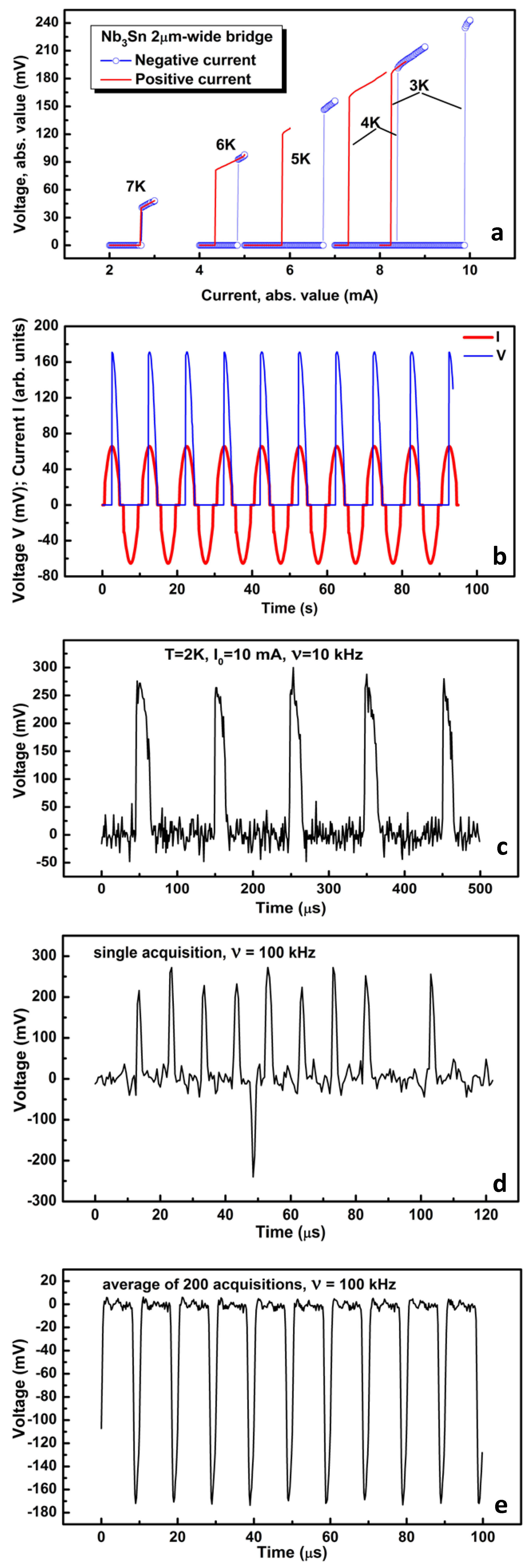
The tests demonstrated , Fig. 1(f), thus indicating the possibility of an SDE. At various temperatures, this type of the -test was systematically performed on a 2 µm bridge and the results are shown in Fig. 2(a). These measurements confirm the fact mentioned in literature that at lower temperatures the difference between the threshold values of and increases with the decreasing bias temperature [5, 23] (the value of corresponds to the current at which the resistive state emerges).
To confirm the expected diode effect, the bridge then was biased at K (PPMS DynaCool cryostat) with external current source and nanovoltmeter (Keithley 6221 and 2182a respectively) applied at frequency 0.1 Hz. Figure 2b demonstrates the result optimized at magnetic field 75 Oe.
Since superconducting diodes are considered to be important elements for electronics, for the majority of applications, it is meaningful to register the effect at possibly higher frequencies. The Keithley current source we used generates AC-currents up to 100 kHz. Corresponding detection of voltage output was performed by an oscilloscope (Tektronix TDS 644A). The results are shown in Fig. 2(c) and (d) for 10 kHz and 100 kHz frequencies, respectively. Higher frequency measurements require specially-designed circuitry in the cryostat since noise becomes an issue, as is seen from the comparison of panel (b) with panels (c) and (d) in Fig. 2. For noise reduction, we plotted 100 kHz data averaged over 200 acquisitions, Fig. 2(e).
IV Discussion
To estimate the frequency range of this type of diode, one needs to understand what the underlying mechanism of the SDE is. As was expected from the general reasons mentioned in Introduction, the effect is nonexistent in the absence of external magnetic field . Comparison of panels (d) and (e) in Fig. 2 shows the change of diode polarity due to the reversal of the external magnetic field from 100 Oe to -100 Oe. The field is orthogonal to the bridge surface. So is the vector of internal magnetic field, , though only at the lateral (top and bottom) edges of the bridge. This field is generated by the current flow through the bridge, with the field lines circulating it. Thus, from symmetry considerations, for an infinitesimally thin bridge, it is orthogonal to the bridge surface at the top and bottom edges. At one edge is parallel, and on the other edge - antiparallel to . Thus, on one of these lateral edges, the amplitudes of external and internal fields add up while on the other edge they subtract. In the AC case, this adding and subtracting reciprocate periodically with frequency :
| (1) |
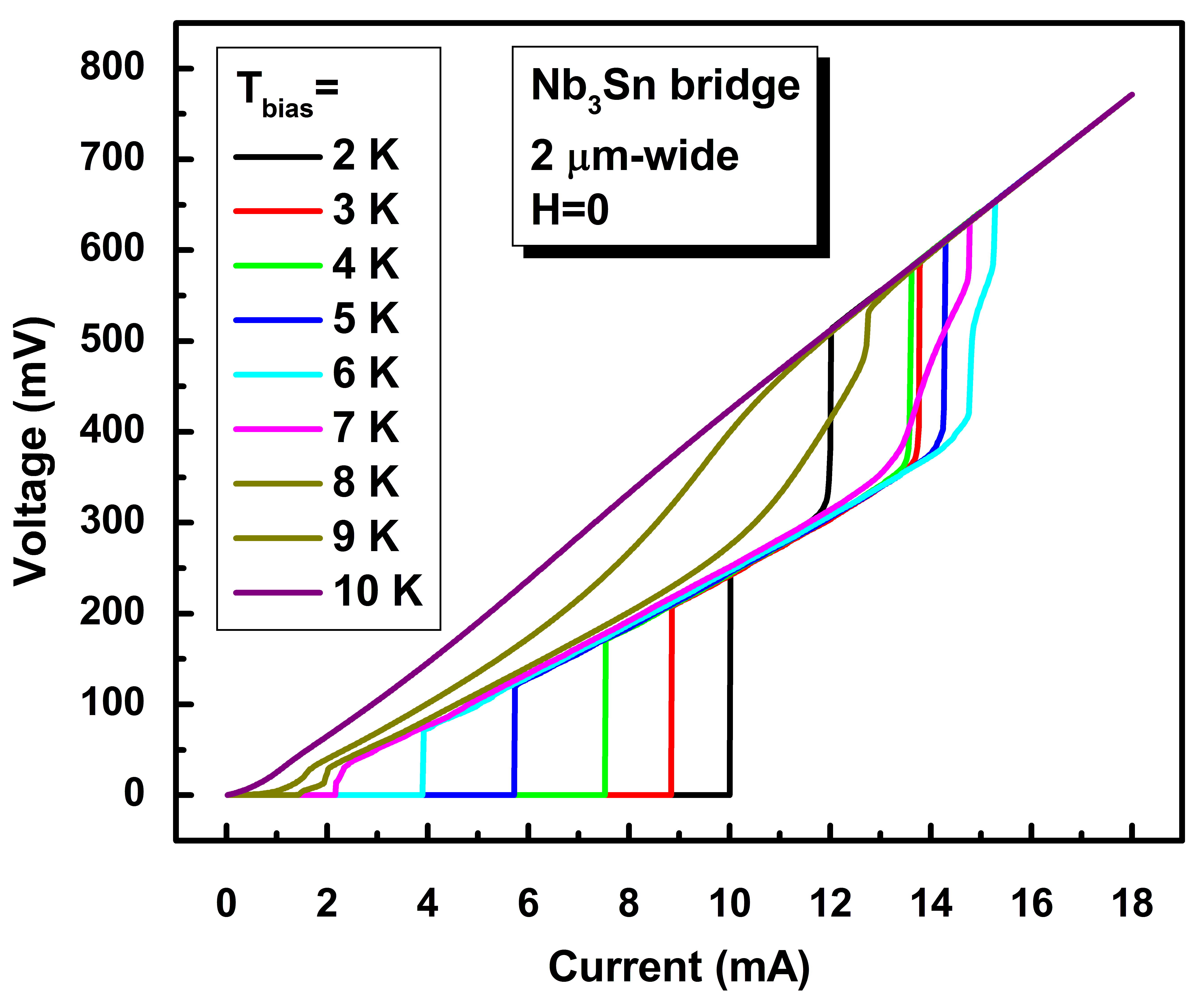
The field amplitude of Oe is optimal for the SDE in our bridges. Higher values ( Oe) quench the effect. The resistive state which yields a non-zero voltage in Fig. 2(c) is caused by vortex motion: the corresponding value of the resistance is a fraction of its normal value. This strongly distinguishes our SDE from the via conformal-mapped nanoholes SDE [31], where the normal state transition stands for the resistance, and flux pinning on defects (nanoholes) secures the lossless current flow, and also breaks the IS. In our case, as follows from Fig. 2(c), the resistance reaches values of 25-40 . At the same time, full transition to the normal state corresponds to the resistance of . Figure 3 depicts a set of measurements at various temperatures. Multiple resistivity jumps are noticeable at lower temperature curves. This step-wise behavior of the curves is explained via vortex pattern rearrangement [34, 35, 36]. Interestingly, Berdiyorov et al. [34] predicted a non-monotonic behavior of critical current of transition from resistive flux-flow state into normal state (calling this current ) for an increase in magnetic field. In our case, a non-monotonic behavior of is observable with the bias temperature. This fact requires explanation via modeling; however, it is beyond the scope of this report.
To explain the results shown in Fig. 2, modeling is necessary which, unlike [31], does not involve a transition into the normal state for resistivity. Using COMSOL Multiphysics, we designed a parameter model [37] in which the IS is geometrically broken: the top edge of the strip has a weaker barrier to vortex penetration than the bottom edge. One can assume, as in the case of NbN SDE [24], that the IS is broken by opposite edges asymmetry caused by physical reasons during the bridge preparation. A closer look at Fig. 1 (d, inset) illustrates the fractal structure of the edge of the current-flow channel. Realistically, the opposite edges are not microscopically symmetric, so our assumption looks quite plausible.
Prior to discussing the details of modeling, we should make one more important remark. Sapphire, which we used as a substrate material, has a very high heat conductivity at low temperatures - much higher than Si, which was used in [31]. This allowed us when modeling to decouple the dynamics of superconducting electrons from the thermal deviation of the lattice from equilibrium. The lattice just serves as an equilibrium heat sink at some effective temperature . The system of time-dependent Ginzburg-Landau (TDGL) equations for the Cooper-pair wave function in the dimensionless form can be presented as (see, e.g., [37]):
| (2) |
| (3) |
| (4) |
| (5) |
Here is the Ginzburg-Landau parameter, is the dimensionless conductivity, is the vector potential (we chose the unit vector to be along the transport current flow in the strip, with orthogonal to it). The parameter , if negative, generates local “weakening” of the superconducting order parameter [37] and, consequently, breaking of the IS. In our model we chose along the top edge within a distance from that edge. Since both superconducting and normal currents are absent across the lateral edges of the strip, we imposed zero-flux conditions for on these boundaries and periodic boundary conditions on transverse facets (i.e., on the boundaries orthogonal to the current flow). Initial conditions for the function should not be identical zero; for example, and may be chosen. Boundary conditions for the component of the vector potential are also periodic on the transverse facets of the strip. On the lateral edges they are which is implemented via the flux-source conditions. Electric field in the chosen gauge for Eqs. (2)-(5) with the zero scalar potential, , is , which means that the solution is an explicit function of time. As soon as this function is known in the whole volume of the strip, one can average over this volume, and determine, up to a constant, the voltage caused by the transport current between the transverse facets of the strip.
The dimensionless spatial distance in the adopted system of equations corresponds to the London penetration depth, , while the dimensionless unit of time has picosecond order of magnitude if K and K.
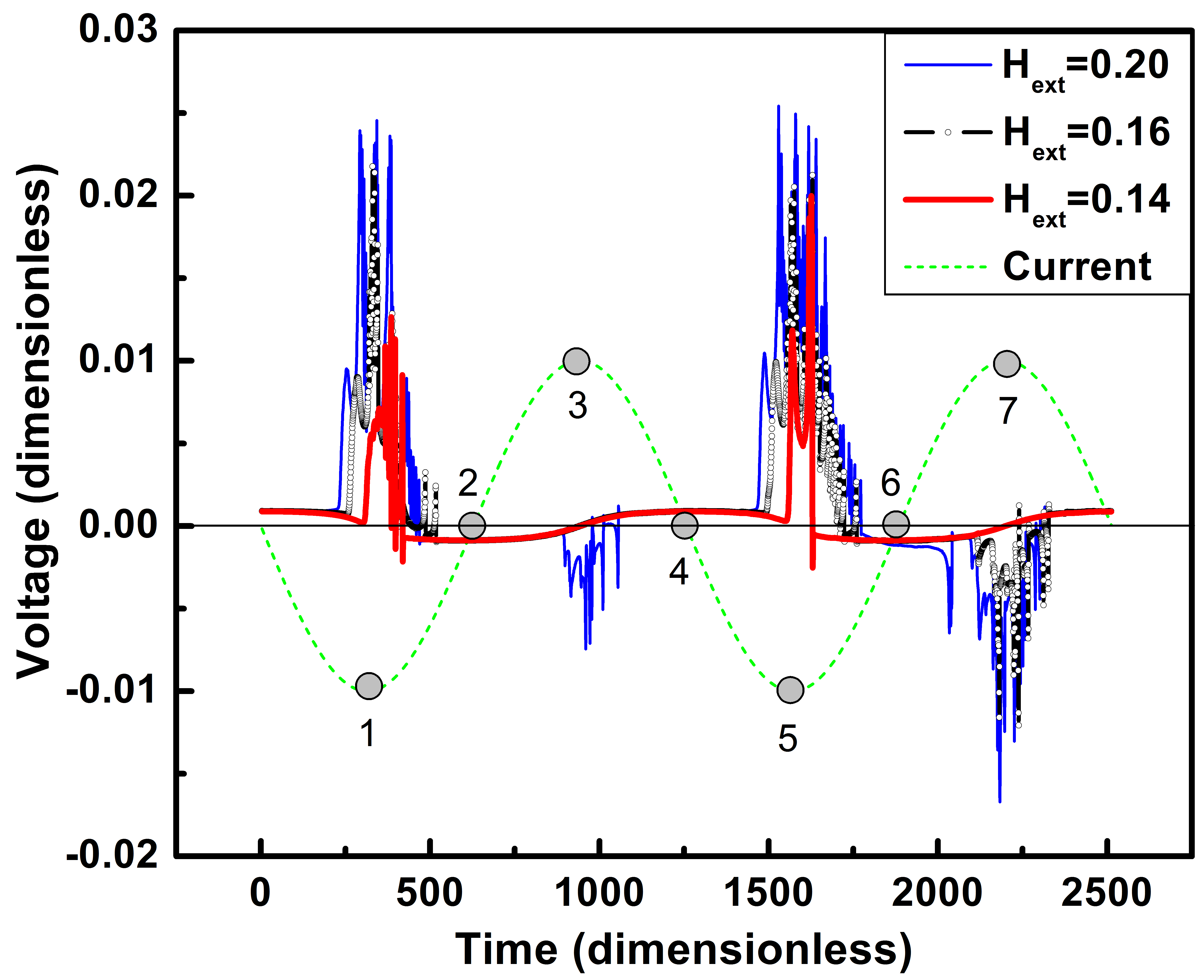
The results of the modeling are shown in Fig. 4. Figure 5 explains the physical mechanism behind the behavior of the voltage in Fig. 4. A video file in the Online Supplemental Materials provides more details related to both of these figures.
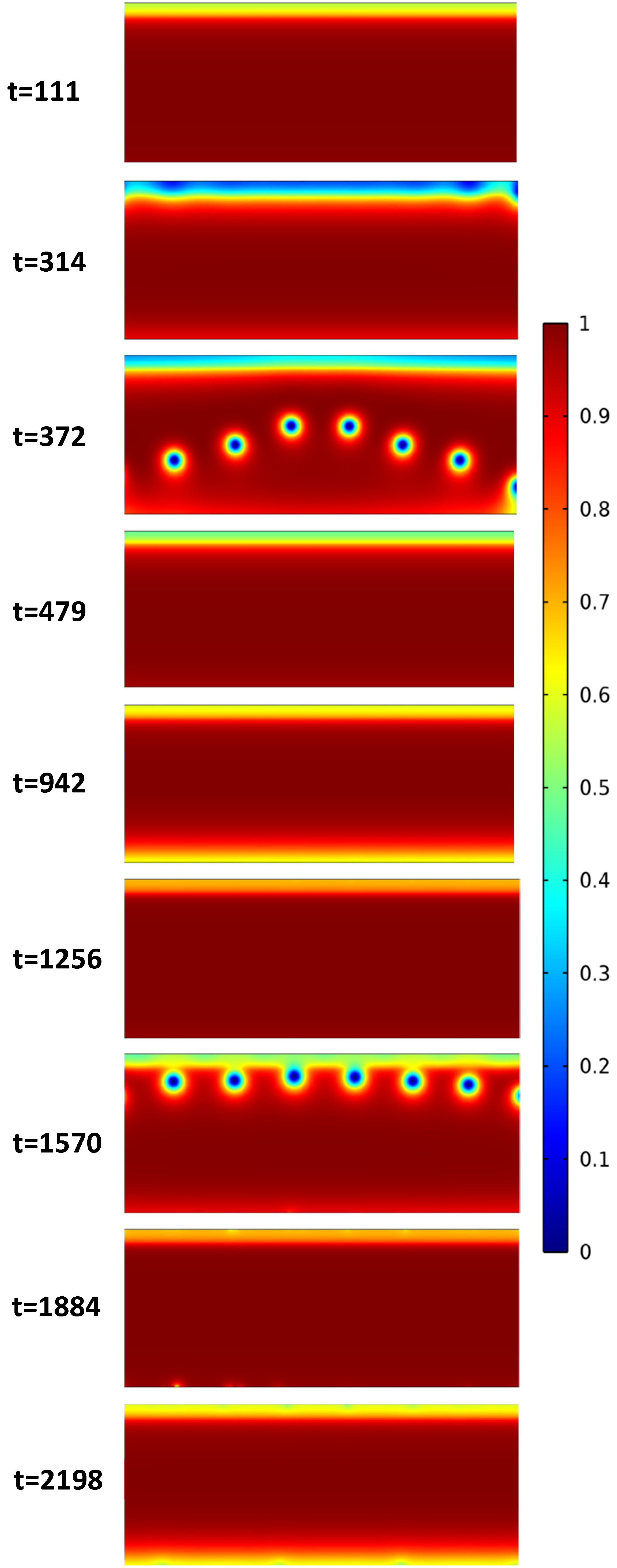
As follows from Fig. 5, for the initial segment of periodic current (say, at ) no fluxons are in the bridge. The current flow is lossless (), and the Cooper pair density is homogeneous within the bridge except the top edge, where it is weakly suppressed due to the asymmetry caused by the parameter, mimicking the IS break. In accordance to Eq. (1), the magnetic field in the top edge of the bridge at this time segment is higher than at the bottom. Tuning the amplitude of the current, or/and the value of external field amplitude , one can exceed the critical value of at the top edge. This allows vortices to start penetrating from the top edge into the bulk of the bridge. The relative values of and should be chosen such that the Lorentz force will be strong enough to move these vortices across the bridge during the first half-period of function. In the second half-period, the value of is larger at the bottom edge. However, because the “rigidity” of this edge (i.e., the Bean-Livingston barrier) is higher, the value of , which was critical for the top edge, is not enough to also be critical for the bottom edge. So even at , when is maximal at the bottom, no vortices penetrate from the bottom (just the density of Cooper pairs is changed a bit). This evolution displayed in Fig. 5 occurs at (and ). If these values are correctly chosen, during the next period the process repeats. In case of improper choices (e.g., or with the same ), diode malfunctioning can occur. This kind of behavior was also noticed during the experiments (see Fig. 2d).
Associating the SDE with the described vortex motion, we can make certain estimates for the performance limits of the SDE in the frequency domain. In the modeled example, the width of the bridge should constitute units of . The angular frequency was chosen to be . It corresponds to frequency 300 MHz. This value is in accordance with our experimental observations. The 100 kHz results have been obtained for a µm-wide bridge. If the geometry is scaled down from 5 µm to 5-50 nm-wide bridges, it can deliver frequencies 2-3 orders of magnitude higher (10-100 MHz range) because of geometric factors affecting their escape time. One can ask: can an even higher frequency range be reached? The answer appears to be yes, due to the following reason: the speed of kinematic vortices is 3 orders of magnitude higher than that of the Abrikosov vortices [38, 39]. If the asymmetry enters the range of kinematic vortices (the highest current jump area in Fig. 3 which corresponds to the transition into normal state), then the operational frequencies of superconducting diodes can reach 100 GHz. Obviously, more research is required to reach that stage experimentally and more modeling is required for better guidance on how to reach this regime.
V Summary
We successfully demonstrated the SDE in ordinary thin superconducting µm-size bridges of Nb3Sn with K. The TRS was broken by external magnetic fields less than 100 Oe, and the IS was broken by structural asymmetry between the bridge edges. High-frequency (up to 100 kHz) diode performance was documented in the time domain and evidence regarding nonequilibrium flux quanta dynamic mechanism of diode action was obtained. Using this evidence, a qualitative explanation of the diode action was obtained via finite element modeling using TDGL equations. Based on both our experimental and modeling results, it is possible to conclude that this kind of SDE can be functional at 2-3 orders higher frequencies than the upper limit of our instrument (100 kHz). With the involvement of kinematic vortices into the diode action, an even higher range of frequencies (of the order of 100 GHz) can be achieved. More experiments guided by modeling can yield two-terminal and multi-terminal high-performance devices for superconducting electronics.
Acknowledgements.
The work of Chapman U. research team is supported by the ONR grants N00014-21-1-2879 and N00014-20-1-2442. We are grateful to Physics Art Frontiers for the provided technical assistance.References
- Gulian et al. [2018] A. M. Gulian, V. R. Nikoghosyan, E. D. Gulian, and G. G. Melkonyan, Quasi-local action of curl-less vector potential on vortex dynamics in superconductors, Physics Letters A 382, 1058 (2018).
- Tokura and Nagaosa [2018] Y. Tokura and N. Nagaosa, Nonreciprocal responses from non-centrosymmetric quantum materials, Nature Communications 9, 3740 (2018).
- Wakatsuki and Nagaosa [2018] R. Wakatsuki and N. Nagaosa, Nonreciprocal Current in Noncentrosymmetric Rashba Superconductors, Phys. Rev. Lett. 121, 026601 (2018).
- Hoshino et al. [2018] S. Hoshino, R. Wakatsuki, K. Hamamoto, and N. Nagaosa, Nonreciprocal charge transport in two-dimensional noncentrosymmetric superconductors, Phys. Rev. B 98, 054510 (2018).
- Ando et al. [2020] F. Ando, Y. Miyasaka, T. Li, J. Ishizuka, T. Arakawa, Y. Shiota, T. Moriyama, Y. Yanase, and T. Ono, Observation of superconducting diode effect, Nature 584, 373 (2020).
- Ideue and Iwasa [2020] T. Ideue and Y. Iwasa, One-way supercurrent achieved in an electrically polar film, Nature 584, 349 (2020).
- Baumgartner et al. [2022a] C. Baumgartner, L. Fuchs, A. Costa, S. Reinhardt, S. Gronin, G. C. Gardner, T. Lindemann, M. J. Manfra, P. E. Faria Junior, D. Kochan, J. Fabian, N. Paradiso, and C. Strunk, Supercurrent rectification and magnetochiral effects in symmetric Josephson junctions, Nature Nanotechnology 17, 39 (2022a).
- Wu et al. [2022] H. Wu, Y. Wang, Y. Xu, P. K. Sivakumar, C. Pasco, U. Filippozzi, S. S. P. Parkin, Y.-J. Zeng, T. McQueen, and M. N. Ali, The field-free Josephson diode in a van der Waals heterostructure, Nature 604, 653 (2022).
- Strambini et al. [2022] E. Strambini, M. Spies, N. Ligato, S. Ilić, M. Rouco, C. González-Orellana, M. Ilyn, C. Rogero, F. S. Bergeret, J. S. Moodera, P. Virtanen, T. T. Heikkilä, and F. Giazotto, Superconducting spintronic tunnel diode, Nature Communications 13, 2431 (2022).
- Wakatsuki et al. [2017] R. Wakatsuki, Y. Saito, S. Hoshino, Y. M. Itahashi, T. Ideue, M. Ezawa, Y. Iwasa, and N. Nagaosa, Nonreciprocal charge transport in noncentrosymmetric superconductors, Science Advances 3, e1602390 (2017).
- Shin et al. [2021] J. Shin, S. Son, J. Yun, G. Park, K. Zhang, Y. J. Shin, J.-G. Park, and D. Kim, Magnetic Proximity-Induced Superconducting Diode Effect and Infinite Magnetoresistance in van der Waals Heterostructure, arXiv.2111.05627 (2021).
- Baumgartner et al. [2022b] C. Baumgartner, L. Fuchs, A. Costa, J. Picó-Cortés, S. Reinhardt, S. Gronin, G. C. Gardner, T. Lindemann, M. J. Manfra, P. E. F. Junior, D. Kochan, J. Fabian, N. Paradiso, and C. Strunk, Effect of Rashba and Dresselhaus spin–orbit coupling on supercurrent rectification and magnetochiral anisotropy of ballistic Josephson junctions, Journal of Physics: Condensed Matter 34, 154005 (2022b).
- Bauriedl et al. [2022] L. Bauriedl, C. Bäuml, L. Fuchs, C. Baumgartner, N. Paulik, J. M. Bauer, K.-Q. Lin, J. M. Lupton, T. Taniguchi, K. Watanabe, C. Strunk, and N. Paradiso, Supercurrent diode effect and magnetochiral anisotropy in few-layer NbSe2, Nature Communications 13, 4266 (2022).
- Yuan and Fu [2022] N. F. Q. Yuan and L. Fu, Supercurrent diode effect and finite-momentum superconductors, Proceedings of the National Academy of Sciences 119, e2119548119 (2022).
- He et al. [2022] J. J. He, Y. Tanaka, and N. Nagaosa, A phenomenological theory of superconductor diodes, New Journal of Physics 24, 053014 (2022).
- Lin et al. [2022] J.-X. Lin, P. Siriviboon, H. D. Scammell, S. Liu, D. Rhodes, K. Watanabe, T. Taniguchi, J. Hone, M. S. Scheurer, and J. I. A. Li, Zero-field superconducting diode effect in small-twist-angle trilayer graphene, Nature Physics (2022).
- Ilić and Bergeret [2022] S. Ilić and F. S. Bergeret, Theory of the Supercurrent Diode Effect in Rashba Superconductors with Arbitrary Disorder, Phys. Rev. Lett. 128, 177001 (2022).
- Karabassov et al. [2022] T. Karabassov, I. V. Bobkova, A. A. Golubov, and A. S. Vasenko, Hybrid helical state and superconducting diode effect in S/F/TI heterostructures, arXiv.2203.15608 (2022).
- Daido et al. [2022] A. Daido, Y. Ikeda, and Y. Yanase, Intrinsic Superconducting Diode Effect, Phys. Rev. Lett. 128, 037001 (2022).
- Anwar et al. [2022] M. S. Anwar, T. Nakamura, R. Ishiguro, S. Arif, J. W. A. Robinson, S. Yonezawa, M. Sigrist, and Y. Maeno, Spontaneous superconducting diode effect in non-magnetic Nb/Ru/Sr2RuO4 topological junctions, arXiv.2211.14626 (2022).
- Souto et al. [2022] R. S. Souto, M. Leijnse, and C. Schrade, The Josephson diode effect in supercurrent interferometers, arXiv.2205.04469 (2022).
- Halterman et al. [2022] K. Halterman, M. Alidoust, R. Smith, and S. Starr, Supercurrent diode effect, spin torques, and robust zero-energy peak in planar half-metallic trilayers, Phys. Rev. B 105, 104508 (2022).
- Hou et al. [2022] Y. Hou, F. Nichele, H. Chi, A. Lodesani, Y. Wu, M. F. Ritter, D. Z. Haxell, M. Davydova, S. Ilić, F. S. Bergeret, A. Kamra, L. Fu, P. A. Lee, and J. S. Moodera, Ubiquitous Superconducting Diode Effect in Superconductor Thin Films, arXiv.2205.09276 (2022).
- Suri et al. [2022] D. Suri, A. Kamra, T. N. G. Meier, M. Kronseder, W. Belzig, C. H. Back, and C. Strunk, Non-reciprocity of vortex-limited critical current in conventional superconducting micro-bridges, Applied Physics Letters 121, 102601 (2022).
- Hope et al. [2021] M. K. Hope, M. Amundsen, D. Suri, J. S. Moodera, and A. Kamra, Interfacial control of vortex-limited critical current in type-II superconductor films, Phys. Rev. B 104, 184512 (2021).
- Vodolazov and Peeters [2005] D. Y. Vodolazov and F. M. Peeters, Superconducting rectifier based on the asymmetric surface barrier effect, Phys. Rev. B 72, 172508 (2005).
- Shmidt [1970a] V. V. Shmidt, The critical current in superconducting films, Sov. Phys. JETP 30, 1137 (1970a).
- Shmidt [1970b] V. V. Shmidt, Critical currents in superconductors, Sov. Phys. Usp. 13, 408 (1970b).
- Bean and Livingston [1964] C. P. Bean and J. D. Livingston, Surface Barrier in Type-II Superconductors, Phys. Rev. Lett. 12, 14 (1964).
- Fossheim and Sudboe [2004] K. Fossheim and A. Sudboe, Superconductivity: Physics and Applications (Wiley, 2004) p. 232.
- Lyu et al. [2021] Y.-Y. Lyu, J. Jiang, Y.-L. Wang, Z.-L. Xiao, S. Dong, Q.-H. Chen, M. V. Milošević, H. Wang, R. Divan, J. E. Pearson, P. Wu, F. M. Peeters, and W.-K. Kwok, Superconducting diode effect via conformal-mapped nanoholes, Nature Communications 12, 2703 (2021).
- Sundahl [2019] C. S. Sundahl, Synthesis of Superconducting Nb3Sn Thin Film Heterostructures for the Study of High-Energy RF Physics, Ph.D. thesis, The University of Wisconsin - Madison, ProQuest Dissertations Publishing, 13805402 (2019).
- Charlesworth et al. [1970] J. P. Charlesworth, I. Macphail, and P. E. Madsen, Experimental work on the niobium-tin constitution diagram and related studies, Journal of Materials Science 5, 580 (1970).
- Berdiyorov et al. [2009] G. R. Berdiyorov, A. K. Elmurodov, F. M. Peeters, and D. Y. Vodolazov, Finite-size effect on the resistive state in a mesoscopic type-II superconducting stripe, Phys. Rev. B 79, 174506 (2009).
- Sánchez-Lotero et al. [2014] P. Sánchez-Lotero, J. Albino Aguiar, and D. Domínguez, Behavior of the flux-flow resistivity in mesoscopic superconductors, Physica C: Superconductivity and its Applications 503, 120 (2014).
- Vodolazov and Peeters [2007] D. Y. Vodolazov and F. M. Peeters, Rearrangement of the vortex lattice due to instabilities of vortex flow, Phys. Rev. B 76, 014521 (2007).
- Gulian [2020] A. Gulian, Shortcut to Superconductivity: Superconducting Electronics via COMSOL Modeling (Springer, 2020).
- Weber and Kramer [1991] A. Weber and L. Kramer, Dissipative states in a current-carrying superconducting film, Journal of Low Temperature Physics 84, 289 (1991).
- Andronov et al. [1993] A. Andronov, I. Gordion, V. Kurin, I. Nefedov, and I. Shereshevsky, Kinematic vortices and phase slip lines in the dynamics of the resistive state of narrow superconductive thin film channels, Physica C: Superconductivity and its Applications 213, 193 (1993).