Angstrom-Scale Imaging of Magnetization in Antiferromagnetic \chFe2As via 4D-STEM
Abstract
We demonstrate a combination of computational tools and experimental 4D-STEM methods to image the local magnetic moment in antiferromagnetic \chFe2As with 6 angstrom spatial resolution. Our techniques utilize magnetic diffraction peaks, common in antiferromagnetic materials, to create imaging modes that directly visualize the magnetic lattice. Using this approach, we show that center-of-mass analysis can determine the local magnetization component in the plane perpendicular to the path of the electron beam. Moreover, we develop Magnstem, a quantum mechanical electron scattering simulation code, to model electron scattering of an angstrom-scale probe from magnetic materials. Using these tools, we identify optimal experimental conditions for separating weak magnetic signals from the much stronger interactions of an angstrom-scale probe with electrostatic potentials. Our techniques should be useful for characterizing the local magnetic order in systems such in thin films, interfaces, and domain boundaries of antiferromagnetic materials, which are difficult to probe with existing methods.
keywords:
antiferromagnetism , 4D-STEM , \chFe2As , magnetic imaging[mse]organization=Department of Materials Science and Engineering, University of Illinois at Urbana-Champaign,city=Urbana, postcode=IL 61801, country=United States
[mrl]organization=Materials Research Laboratory, University of Illinois at Urbana-Champaign,city=Urbana, postcode=IL 61801, country=United States
[ncsa]organization=National Center for Supercomputing Applications, University of Illinois at Urbana-Champaign,city=Urbana, postcode=IL 61801, country=United States
1 Introduction
For decades, transmission electron microscopy (TEM) and scanning TEM (STEM) methods such as Lorentz TEM, electron holography, and differential phase contrast (DPC) have provided valuable insight into the magnetic structure of materials on the micro and nanoscales. The relatively high spatial resolution of these methods, which is typically 5-20 nanometers (nm), but can reach up to around 1 nm [1], have made them valuable for uncovering variations in the local magnetization such as domain walls in ferromagnets, skyrmions, and the magnetization of nanoparticles and thin films. As TEM-based techniques continue to improve, a natural question is whether electron microscopy techniques can be extended to probe local magnetization on the atomic scale.
Antiferromagnets such as \chFe2As (Figure 1b) have received renewed interest as potential materials to increase the speed and density of spintronic devices because they exhibit terahertz spin dynamics, have low magnetic susceptibility, and lack stray fields. Because their local magnetization varies periodically on the scale of a few angstroms, antiferromagnets offer ideal systems to test methods for atomic scale magnetic characterization. New TEM-based magnetic imaging techniques could directly probe magnetic ordering in antiferromagnets in real space, complementing bulk characterization methods such as neutron diffraction [2], while also achieving the high spatial resolution of surface sensitive techniques such as spin-polarized scanning tunneling microscopy[3].
Yet, few TEM studies have been attempted to image antiferromagnetic order. Part of the challenge is spatial resolution: a few-nanometer electron beam would average over several magnetic unit cells in most antiferromagnets, producing no net magnetic deflection. Sensitivity is another: for techniques such as DPC that detect magnetization as a deflection of the electron beam, the minimum detectable deflection is inversely proportional to probe size[4, 5]. This trade-off between spatial resolution and sensitivity to magnetic fields makes it difficult to detect magnetic signals at atomic length scales. A third and particularly insidious challenge for electron microscopy is that magnetization in antiferromagnets varies on the same length scale as the atomic spacings in materials, making it exceptionally difficult to isolate magnetic signals from scattering effects from the crystallographic lattice. Recently, DPC-STEM has been used to probe antiferromagnetism across a domain wall [6] and, via kernel filtering and unit-cell averaging, has recently been used to map the magnetic structure of an antiferromagnet in real space [7]. However, these methods remain somewhat indirect, and the detection mechanisms behind these recent observations and how magnetic signals can be reliably separated from atomic structure remain unclear. By collecting the full diffraction pattern, four-dimensional (4D) STEM studies can provide greater measurement flexibility and insight into the effect of magnetism on electron scattering. Here, we use the latest generation of direct electron detectors for 4D-STEM, combined with electron scattering simulations to model, measure, and extract the local magnetization on the few-angstrom scale.
2 Results and Discussion
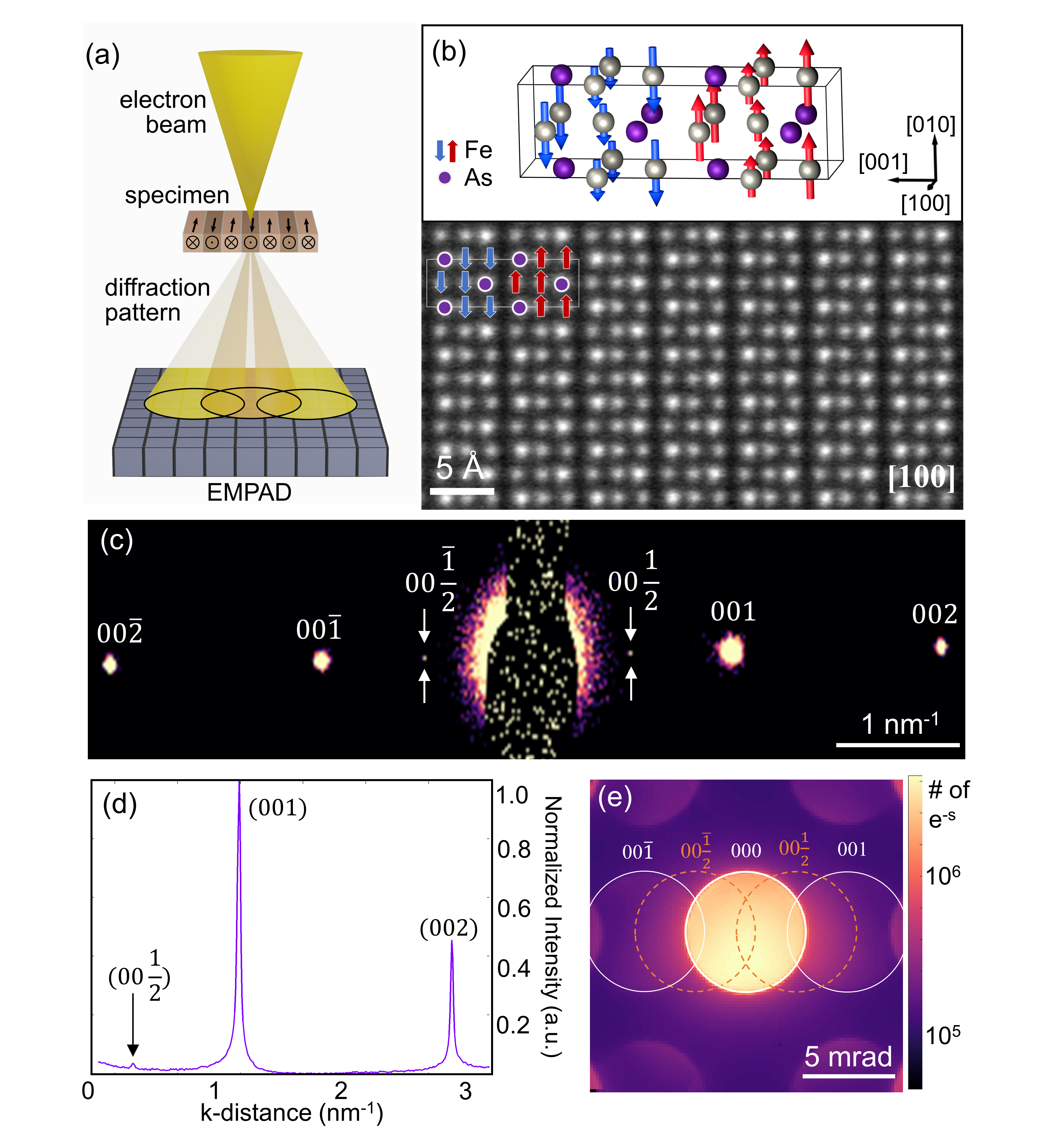
We demonstrate our approach on \chFe2As, a collinear, metallic antiferromagnet with a Néel temperature of . Figure 1b shows the structure of \chFe2As: it has a tetragonal crystal structure (, ) [8]. The Néel vector for \chFe2As can lie along either of the crystallographically equivalent or axes, and the magnetic unit cell has dimensions . Single crystals of Fe2As were grown by slow-cooling stoichiometric mixtures of the elements from the melt at 1000 °C in fused silica ampoules, following the detailed procedure in Ref. 9. Then, TEM specimens of \chFe2As were prepared using standard focused ion beam lift-out procedures and imaged with aberration-corrected STEM. Figure 1b shows an annular dark-field STEM image of \chFe2As along the [100] zone axis. In this orientation, vertical blocks three atoms wide, or “trilayers” are visible. Within each -wide trilayer, the magnetic moments of the Fe atoms are aligned parallel, while the magnetic moments of adjacent trilayers are antiparallel.
2.1 Selected area electron diffraction
We first confirm that antiferromagnetic ordering can be detected in our sample. Figure 1c shows a room temperature selected area electron diffraction (SAED) pattern of \chFe2As along the [100] zone (see full diffraction pattern in Figure S1). While the brightest peaks in the diffraction pattern arise from Bragg diffraction from the crystal, we also observe weak diffraction spots (white arrows in Figure 1c) with an intensity of roughly 1/20 to 1/300 of the diffraction spots (Figure 1d), depending on the region and sample thickness measured. These magnetic diffraction peaks correspond to the length of the magnetic unit cell. Similar half-order peaks have been previously observed in electron beam diffraction of antiferromagnetic \chNiO [10], and magnetic diffraction peaks with fractional k-vectors are also routinely observed in neutron diffraction studies of antiferromagnets, where they are used to determine magnetic structures. Importantly, the presence of the spots in the SAED pattern demonstrates that antiferromagnetic ordering is detectable in our \chFe2As sample.
2.2 Experimental 4D-STEM
Next, we extend our measurements to the atomic scale using 4D-STEM. In 4D-STEM, an angstrom to nanoscale electron beam is rastered across a sample, and a convergent beam electron diffraction (CBED) pattern is collected at each scan position (Figure 1a). When combined with a new generation of fast, high-dynamic range direct electron detectors, 4D-STEM offers new opportunities to probe the structure and functional properties of materials at the atomic scale. A key advantage of 4D-STEM is that it collects the two-dimensional (2D) electron scattering distribution as a function of position, offering atomic-scale resolution while also providing more flexibility to extract and isolate signals of interest. This property has enabled measurements of angstrom-scale electrostatic fields, such as the local polarization of ferroelectrics [11, 12, 13] as well as nanoscale mapping of magnetic fields[5].
To acquire our 4D-STEM data, we used a Thermo Fisher Titan equipped with an electron microscope pixel array detector (EMPAD), a 128128 pixel direct electron detector with a high dynamic range of 1,000,000:1[14]. This high dynamic range allows us to achieve high signal-to-noise ratios and detect small intensity changes from magnetism[5]. We used an acceleration voltage of 120 kilovolts (kV) and a semi-convergence angle of 3.5 milliradians (mrad), yielding a probe size of approximately . This probe size was chosen to approximately match the width of the trilayers and the length scale of magnetization variations in our specimen. As we discuss later, this convergence angle maximizes the magnetic signal. We also operated with the objective lens on, rather than in a Lorentz or field-free mode. In this mode, the objective lens produces a magnetic field of 1.61 T normal to the sample plane, which should orient the Fe2As moments in-plane, perpendicular to the beam direction[15]. We calibrated the strength of the objective lens using Hall probe measurements reported in Ref. 5. Figure 1e shows a position averaged CBED pattern of \chFe2As along the [100] zone axis captured using 4D-STEM. The CBED pattern contains similar information to the SAED pattern in Figure 1c, but the use of a convergent beam results in the formation of diffraction disks, rather than spots. As we show below, while the magnetic reflections are too weak to be directly visible in the CBED pattern (Figure 1e), they nevertheless produce measurable signals that enable atomic scale magnetic imaging.
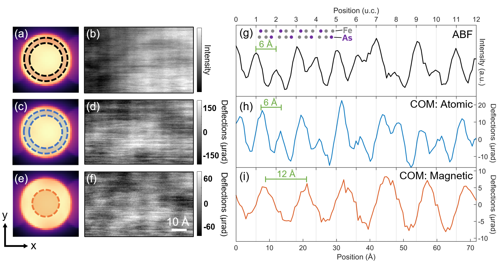
In Figure 2, we extracted three signals of interest from a 4D-STEM dataset. First, we created a virtual annular bright field (ABF) image by applying a digital mask (Figure 2a) to each CBED pattern and integrating the counts within the virtual detector at each scan position. The resulting image (Figure 2b) is similar to that generated by a conventional physical ABF STEM detector; dark vertical lines correspond to the locations of trilayers. Compared to the ADF STEM image in Figure 1b, the contrast in the virtual ABF image is inverted because of the different choice of collection angles and the image resolution is decreased due to the relatively large probe size.
In Figure 2c-f, we apply center-of-mass (COM) analysis to our 4D-STEM data to separate and isolate signals from the crystal lattice and magnetic structure. COM analysis measures the center of mass of the intensity of the diffraction patterns acquired via 4D-STEM. When applied to the full diffraction pattern, the COM measures changes to the average momentum of the electron beam produced by its interactions with the specimen; correspondingly, COM analysis is commonly used to measure electric fields and magnetic domains [16, 17, 5]. In addition, application of COM analysis to selected regions of the CBED pattern has been shown to be an effective method to separate scattering phenomena that dominate different regions of reciprocal space [5].
While the COM is a 2D vector quantity, we focus here on a single component, COM shifts along the -axis direction, since we expect that both the electrostatic and magnetic fields of \chFe2As will produce COM deflections along this direction. Orienting the real space images and diffraction pattern so that the axis points in the x-direction, we calculate the shifts in regions of the diffraction pattern defined by the masks shown in Figure 2c,e, creating the COM images in Figure 2d,f. Figure 2g-i show background subtracted line profiles of the virtual ABF (Figure 2g) and two COM images (Figure 2h,i). Both the ABF line profile in Figure 2g and the COM data in Figure 2h reveal lattice fringes with the periodicity of the trilayers of the structural unit cell. The COM signal in Figure 2i is especially interesting: it alternates in direction from one trilayer to the next, and exhibits a periodicity. As we show in Figure S3, these fringes can also be detected using DPC imaging using a virtual quadrant detector. The position and frequency of this COM signal are an excellent match for the local magnetization changes expected for antiferromagnetic \chFe2As, a strong indicator that our data represents an experimental detection of the atomic scale antiferromagnetic ordering.
2.3 4D-STEM simulations using Magnstem
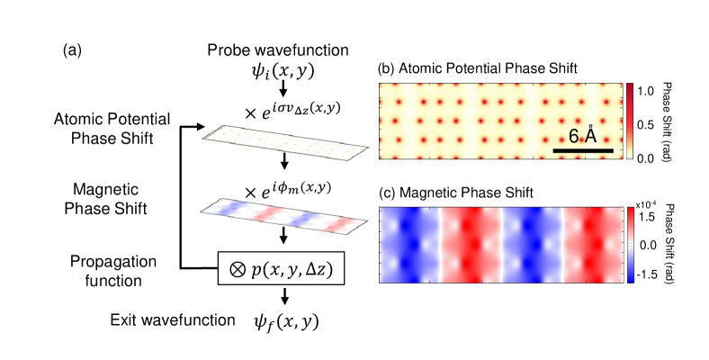
To understand the origins of these signals, we developed Magnstem, a quantitative simulation code to model the electron scattering of an angstrom-scale probe in magnetic materials. We based our methods on multislice [18], a powerful approach for simulating TEM experiments and calculating the dynamic scattering of the electron beam from electrostatic fields in the specimen. In multislice, the sample is divided into thin slices and the electron wave function is alternately scattered by the transmission function of a slice and propagated towards the next slice, as shown in Figure 3a. While multislice simulations typically focus only on scattering from the screened nuclear potential, a few groups have adapted multislice codes to incorporate scattering from magnetic fields [19, 20, 21, 22].
In Magnstem, we describe the evolution of the probe wavefunction as follows:
| (1) |
Here, the effect of magnetic fields within the plane of the sample enters through the component of the vector potential along the propagation direction . We retain only the term from the full paraxial Pauli equation for a magnetic sample (Eq. (3) in Ref. 21) because this term is two orders of magnitude larger than other terms that describe the interaction between electrons and magnetic fields when the spins are oriented perpendicular to the electron beam (see the Supplementary Material). Equation 1 can then be modeled using the conventional multislice method using the following transmission function for a slice of the sample,
| (2) |
where .
To implement this method, we modified the Kirkland multislice code [23], adding a contribution to the transmission function due to (shown in Figure 3c), which we derived from magnetization densities calculated for \chFe2As using density-functional theory [9] (see the Supplementary Material). Magnstem adds to conventional multislice, where the electron beam undergoes phase shifts due to scattering from atomic potentials (Figure 3b), by incorporating an additional phase shift due to the in-plane magnetic moments of the sample (Figure 3c). As Figure 3b-c show, the additional phase shift due to magnetic moments is small: 1,000 to 10,000 times smaller than the phase shift due to atomic moments.
We next use Magnstem to simulate 4D-STEM datasets, matching key parameters of simulation to experiment (see the Supplementary Material). We simulate \chFe2As down the [100] direction with a thickness of 9.1 nm (25 unit cells), creating a 4D dataset by rastering the simulated probe over probe positions, saving the CBED pattern at each probe position. To account for atomic vibrations, the frozen phonon approximation was employed [24], with each CBED pattern averaged over 10 frozen phonon configurations. We note that this approach is distinct from the finite difference technique to compute phonon properties of materials from first-principles [25], sometimes also referred to as frozen-phonon method. To isolate the impact of antiferromagnetism on electron scattering, we conducted two sets of 4D-STEM simulations with the magnetism turned either on or off, then used principal component analysis (PCA) to analyze the resulting CBED patterns (Figure 4).
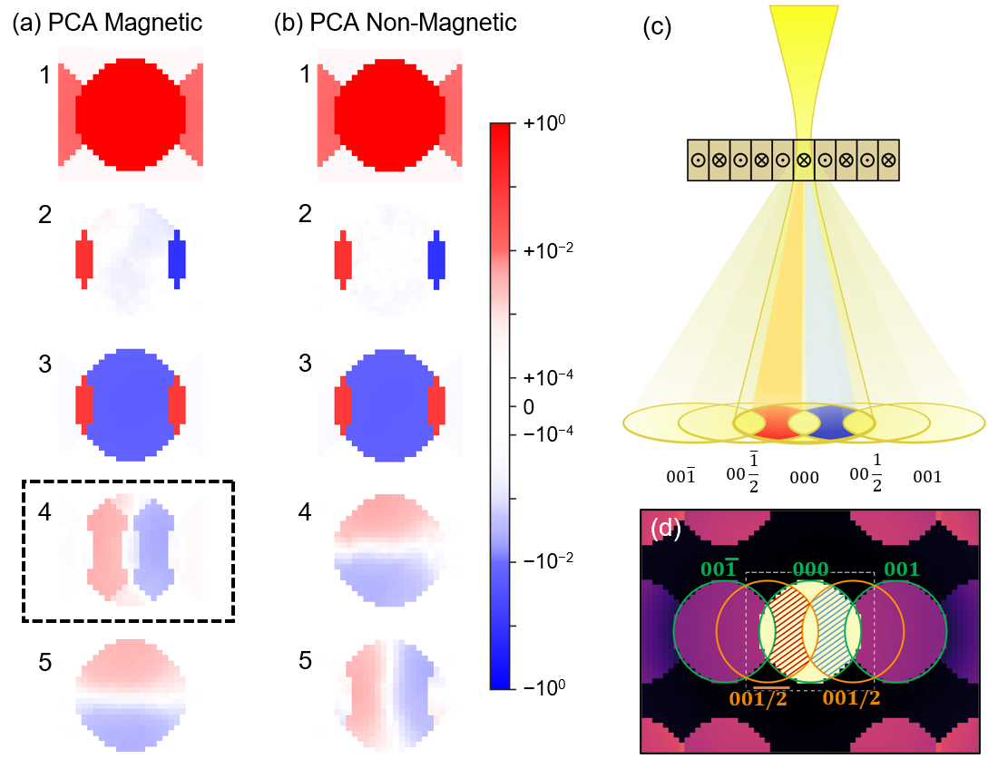
Figures 4a-b show the principal components for the two 4D-STEM data sets. Comparing the magnetic and non-magnetic simulations, the first three principal components and their corresponding real-space maps are nearly identical, indicating they arise primarily from the atomic lattice of the material (see Figure S4 for PCA components, singular values, and corresponding real space maps). Accordingly, real space maps of the first three PCA components (Figure S4) each produce (001) lattice fringes with the periodicity of the crystallographic unit cell.
Notably, we find that the fourth PCA component of the magnetic simulations (Figure 4a, black dashed box) provides the basis for angstrom-scale STEM imaging of antiferromagnetism. The shape and symmetry of this component, which is absent in the non-magnetic simulations, corresponds to regions of overlap between the BF disk and the magnetic disks (Figure 4c-d). In addition, real space maps for this component (Figure S4) show lattice fringes with the periodicity of the magnetic unit cell.
These results are important because they explain the physical origin behind angstrom-scale detection of antiferromagnetism and illustrate how to set up direct imaging modes for magnetic lattice fringes. In short, the periodic magnetic structure of \chFe2As acts as a weak phase grating, producing disks. When these magnetic reflections overlap with the direct beam, they produce magnetic lattice fringes–a direct parallel to how overlap between structural Bragg disks gives rise to structural lattice fringes. Notably, this mechanism is distinct from the conventional mechanisms used to explain Lorentz TEM and STEM signals for ferromagnetic materials, where slowly varying magnetic fields produce rigid shifts of the entire diffraction pattern. The semi-convergence angle has a strong impact on the interpretability and strength of the magnetic signal. We show using Magnstem simulations (Figure S5) that the magnetic signals are strongest when the probe size is approximately wide, matching the length scale of the magnetic columns in the sample. This can also be understood in terms of the diffraction pattern: magnetic contrast arises from overlap of the magnetic disks with the BF disk, and this probe size maximizes that overlap (Figure S6).
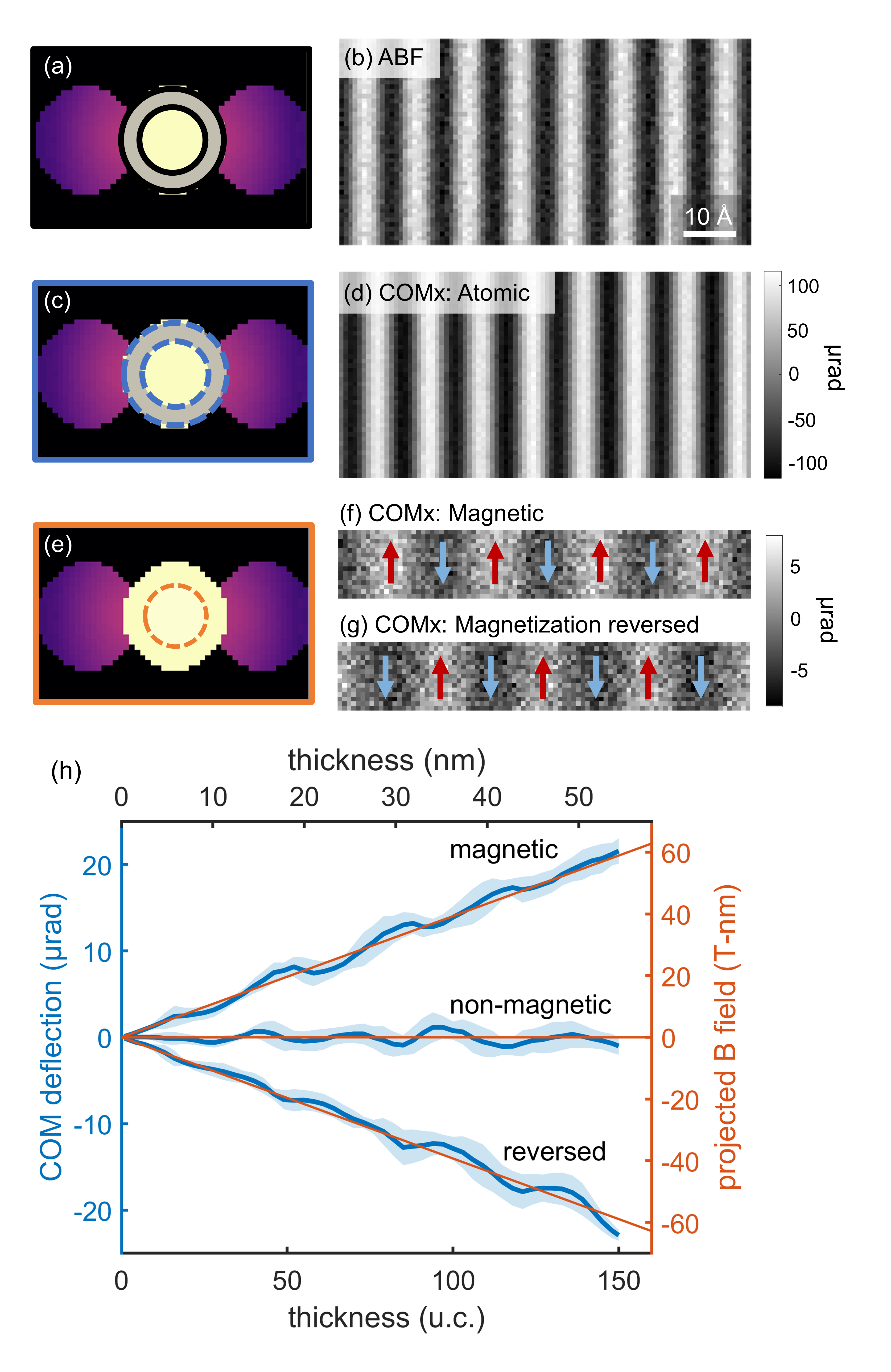
Finally, we performed COM analyses of the 4D-STEM simulations, mirroring the processing approach used for experimental data. Unlike in simulations, we found that a simple PCA analysis was not sufficient to isolate the magnetic signal in experimental data. This is likely because CBED patterns from experimental samples contain spatially-varying components due to sample preparation and beam damage making it difficult to isolate the weaker magnetic contributions in the CBED patterns. Overall, our simulations are an excellent match for the experimental data in Figure 2. In contrast to PCA, we found COM imaging using selected regions of the BF disk to be a robust approach for isolating magnetism in both experiment and simulations. Moreover, we show in Figure 5f-g that COM analysis can unambiguously determine the sign of the in-plane component of magnetic moment (for example, the up vs. down arrows in Figure 5f). This ability arises from the asymmetry of the phase between the peaks and the corresponding intensity asymmetry of the magnetic PCA component in Figure 4.
In TEM imaging of crystalline samples, lattice fringes arising from the atomic structure have been observed to reverse in contrast as the sample thickness changes. Thus, proper interpretation of the magnetic signal requires understanding how it scales with sample thickness. We simulated 4D-STEM data sets over a range of thicknesses, from 0.36 nm to 54.3 nm (Figure 5h) and measured the intensity of magnetism-induced COM shifts in the overlap region (Figure 5e). Figure 5h shows that the COMx signal increases approximately linearly with the sample thickness and projected magnetic field. These results show that it is advantageous to use a thicker specimen to maximize the magnetic signal, without potential complications from contrast reversal.
3 Conclusions
In summary, we developed an approach for imaging the magnetic structure of antiferromagnets in real space using 4D-STEM. In our work, to increase the signal from the magnetic structure, we match the size of the electron probe to the size of regions of aligned spins. Using Magnstem simulations, we observe that the periodic magnetic structure of \chFe2As redistributes intensity in CBED patterns at the overlap of antiferromagnetic disks with the BF disk. By selecting those regions within the BF disk, COM imaging can be used to detect the magnetic structure of \chFe2As. This approach can be broadly applied to antiferromagnets whose magnetic structures produce fractional antiferromagnetic reflections, and should allow for the determination of magnetic structure in antiferromagnetic thin films and imaging of antiferromagnetic domains, antiphase boundaries, and domain walls.
Declaration of Competing Interest
KXN is a co-inventor on the license for the EMPAD detector to Thermo Fisher Scientific.
Acknowledgements
The authors thank D. A. Muller for useful discussions. This work was supported by the Air Force Office of Scientific Research under award number FA9550-20-1-0302. K.X.N. is also supported in part by the L’Oreal For Women in Science Postdoctoral Fellowship. J.H. is partially supported by the DIGI-MAT program through National Science Foundation under Grant No. 1922758. Electron microscopy facilities were provided by the University of Illinois Materials Research Laboratory and the Cornell Center for Materials Research through the National Science Foundation MRSEC program through award DMR-1719875. The crystal growth and density functional calculations were supported by the Illinois Materials Research Science and Engineering Center through the National Science Foundation MRSEC program, award DMR-1720633. This work made use of the Illinois Campus Cluster, a computing resource that is operated by the Illinois Campus Cluster Program (ICCP) in conjunction with the National Center for Supercomputing Applications (NCSA) and which is supported by funds from the University of Illinois at Urbana-Champaign.
Supplementary materials
Supplementary material, including Material and Methods and additional figures, are appended to the end of this manuscript file.
References
-
[1]
V. Boureau, M. Staňo, J.-L. Rouvière, J.-C. Toussaint, O. Fruchart,
D. Cooper,
High-sensitivity
mapping of magnetic induction fields with nanometer-scale resolution:
comparison of off-axis electron holography and pixelated differential phase
contrast, Journal of Physics D: Applied Physics 54 (2021) 085001.
doi:10.1088/1361-6463/abc77d.
URL https://iopscience.iop.org/article/10.1088/1361-6463/abc77d - [2] M. Schlenker, J. Baruchel, Possibilities of x-ray and neutron topography for domain and phase coexistence observations, Ferroelectrics 162 (1) (1994) 299–306. doi:10.1080/00150199408245118.
-
[3]
M. Enayat, Z. Sun, U. R. Singh, R. Aluru, S. Schmaus, A. Yaresko, Y. Liu,
C. Lin, V. Tsurkan, A. Loidl, J. Deisenhofer, P. Wahl,
Real-space
imaging of the atomic-scale magnetic structure of Fe1+yTe, Science
345 (6197) (2014) 653–656.
doi:10.1126/science.1251682.
URL https://science.sciencemag.org/content/345/6197/653 -
[4]
J. Chapman, P. Batson, E. Waddell, R. Ferrier,
The
direct determination of magnetic domain wall profiles by differential phase
contrast electron microscopy, Ultramicroscopy 3 (1978) 203–214.
doi:https://doi.org/10.1016/S0304-3991(78)80027-8.
URL https://www.sciencedirect.com/science/article/pii/S0304399178800278 -
[5]
K. X. Nguyen, X. S. Zhang, E. Turgut, M. C. Cao, J. Glaser, Z. Chen, M. J.
Stolt, C. S. Chang, Y.-T. Shao, S. Jin, G. D. Fuchs, D. A. Muller,
Disentangling
magnetic and grain contrast in polycrystalline thin
films using four-dimensional lorentz scanning transmission electron
microscopy, Phys. Rev. Applied 17 (2022) 034066.
doi:10.1103/PhysRevApplied.17.034066.
URL https://link.aps.org/doi/10.1103/PhysRevApplied.17.034066 -
[6]
F. Krizek, S. Reimers, Z. Kašpar, A. Marmodoro, J. Michalička, O. Man,
A. Edström, O. J. Amin, K. W. Edmonds, R. P. Campion, F. Maccherozzi, S. S.
Dhesi, J. Zubáč, D. Kriegner, D. Carbone, J. Železný, K. Výborný,
K. Olejník, V. Novák, J. Rusz, J.-C. Idrobo, P. Wadley, T. Jungwirth,
Atomically
sharp domain walls in an antiferromagnet, Science Advances 8 (13) (2022)
eabn3535.
arXiv:https://www.science.org/doi/pdf/10.1126/sciadv.abn3535, doi:10.1126/sciadv.abn3535.
URL https://www.science.org/doi/abs/10.1126/sciadv.abn3535 -
[7]
Y. Kohno, T. Seki, S. D. Findlay, Y. Ikuhara, N. Shibata,
Real-space
visualization of intrinsic magnetic fields of an antiferromagnet, Nature
602 (7896) (2022) 234–239.
doi:10.1038/s41586-021-04254-z.
URL https://www.nature.com/articles/s41586-021-04254-z -
[8]
K. Hisao, A. Norio, The Magnetic
Structure of Fe2As, Journal of the Physical Society of Japan 21 (11) (1966)
2238–2243.
doi:10.1143/JPSJ.21.2238.
URL https://doi.org/10.1143/JPSJ.21.2238 -
[9]
K. Yang, K. Kang, Z. Diao, A. Ramanathan, M. H. Karigerasi, D. P. Shoemaker,
A. Schleife, D. G. Cahill,
Magneto-optic
response of the metallic antiferromagnet to
ultrafast temperature excursions, Phys. Rev. Materials 3 (2019) 124408.
doi:10.1103/PhysRevMaterials.3.124408.
URL https://link.aps.org/doi/10.1103/PhysRevMaterials.3.124408 -
[10]
J. C. Loudon,
Antiferromagnetism
in nio observed by transmission electron diffraction, Phys. Rev. Lett. 109
(2012) 267204.
doi:10.1103/PhysRevLett.109.267204.
URL https://link.aps.org/doi/10.1103/PhysRevLett.109.267204 -
[11]
A. K. Yadav, K. X. Nguyen, Z. Hong, P. García-Fernández,
P. Aguado-Puente, C. T. Nelson, S. Das, B. Prasad, D. Kwon, S. Cheema, A. I.
Khan, C. Hu, J. Íñiguez, J. Junquera, L.-Q. Chen, D. A. Muller,
R. Ramesh, S. Salahuddin,
Spatially resolved
steady-state negative capacitance, Nature 565 (7740) (2019) 468–471.
doi:10.1038/s41586-018-0855-y.
URL https://doi.org/10.1038/s41586-018-0855-y -
[12]
K. Moore, U. Bangert, M. Conroy,
Aberration corrected stem techniques
to investigate polarization in ferroelectric domain walls and vortices, APL
Materials 9 (2) (2021) 020703.
arXiv:https://doi.org/10.1063/5.0035958, doi:10.1063/5.0035958.
URL https://doi.org/10.1063/5.0035958 - [13] C. Ophus, Four-dimensional scanning transmission electron microscopy (4d-stem): From scanning nanodiffraction to ptychography and beyond, Microscopy and Microanalysis 25 (3) (2019) 563–582. doi:10.1017/S1431927619000497.
- [14] M. W. Tate, P. Purohit, D. Chamberlain, K. X. Nguyen, R. Hovden, C. S. Chang, P. Deb, E. Turgut, J. T. Heron, D. G. Schlom, et al., High dynamic range pixel array detector for scanning transmission electron microscopy, Microscopy and Microanalysis 22 (1) (2016) 237–249. doi:10.1017/S1431927615015664.
-
[15]
K. Yang, K. Kang, Z. Diao, M. H. Karigerasi, D. P. Shoemaker, A. Schleife,
D. G. Cahill,
Magnetocrystalline
anisotropy of the easy-plane metallic antiferromagnet
, Phys. Rev. B 102 (2020) 064415.
doi:10.1103/PhysRevB.102.064415.
URL https://link.aps.org/doi/10.1103/PhysRevB.102.064415 -
[16]
K. Müller, F. F. Krause, A. Béché, M. Schowalter, V. Galioit, S. Löffler,
J. Verbeeck, J. Zweck, P. Schattschneider, A. Rosenauer,
Atomic electric fields revealed by
a quantum mechanical approach to electron picodiffraction, Nature
Communications 5 (2014) 1–8.
doi:10.1038/ncomms6653.
URL https://doi.org/10.1038/ncomms6653 - [17] M. C. Cao, Y. Han, Z. Chen, Y. Jiang, K. X. Nguyen, E. Turgut, G. D. Fuchs, D. A. Muller, Theory and practice of electron diffraction from single atoms and extended objects using an EMPAD, Microscopy 67 (December 2017) (2018) i150–i161. doi:10.1093/jmicro/dfx123.
- [18] J. M. Cowley, A. F. Moodie, The scattering of electrons by atoms and crystals. I. A new theoretical approach, Acta Crystallographica 10 (10) (1957) 609–619. doi:10.1107/s0365110x57002194.
- [19] A. Rother, K. Scheerschmidt, Relativistic effects in elastic scattering of electrons in TEM, Ultramicroscopy 109 (2) (2009) 154–160. doi:10.1016/j.ultramic.2008.08.008.
- [20] V. Grillo, L. Marrucci, E. Karimi, R. Zanella, E. Santamato, Quantum simulation of a spin polarization device in an electron microscope, New Journal of Physics 15 (2013). doi:10.1088/1367-2630/15/9/093026.
- [21] A. Edström, A. Lubk, J. Rusz, Elastic Scattering of Electron Vortex Beams in Magnetic Matter, Physical Review Letters 116 (12) (2016) 1–5. arXiv:1509.00744, doi:10.1103/PhysRevLett.116.127203.
-
[22]
A. Edström, A. Lubk, J. Rusz,
Quantum mechanical
treatment of atomic-resolution differential phase contrast imaging of
magnetic materials, Phys. Rev. B 99 (2019) 174428.
doi:10.1103/PhysRevB.99.174428.
URL https://link.aps.org/doi/10.1103/PhysRevB.99.174428 -
[23]
E. J. Kirkland,
Advanced Computing
in Electron Microscopy, Springer US, Boston, MA, 2010.
doi:10.1007/978-1-4419-6533-2.
URL http://link.springer.com/10.1007/978-1-4419-6533-2 -
[24]
E. J. Kirkland,
Advanced Computing
in Electron Microscopy, Springer US, Boston, MA, 2010, Ch. 7, pp. 183–184.
doi:10.1007/978-1-4419-6533-2.
URL http://link.springer.com/10.1007/978-1-4419-6533-2 -
[25]
K. Kunc, Recent
Results in Semiconductor Dynamics by Ab Initio ‘Direct’ Approach, in:
Electronic Structure, Dynamics, and Quantum Structural Properties of
Condensed Matter, Springer US, Boston, MA, 1985, pp. 227–312.
doi:10.1007/978-1-4757-0899-8\_6.
URL http://link.springer.com/10.1007/978-1-4757-0899-8_6