Impact of junction length on supercurrent resilience against magnetic field in InSb-Al nanowire Josephson junctions
Abstract
Semiconducting nanowire Josephson junctions represent an attractive platform to investigate the anomalous Josephson effect and detect topological superconductivity by studying Josephson supercurrent. However, an external magnetic field generally suppresses the supercurrent through hybrid nanowire junctions and significantly limits the field range in which the supercurrent phenomena can be studied. In this work, we investigate the impact of the length of InSb-Al nanowire Josephson junctions on the supercurrent resilience against magnetic fields. We find that the critical parallel field of the supercurrent can be considerably enhanced by reducing the junction length. Particularly, in -long junctions supercurrent can persist up to parallel field - approaching the critical field of the superconducting film. Furthermore, we embed such short junctions into a superconducting loop and obtain the supercurrent interference at a parallel field of . Our findings are highly relevant for multiple experiments on hybrid nanowires requiring a magnetic field-resilient supercurrent.
keywords:
seconductor nanowire, Josephson junction, magnetic field, resilient supercurrentQuTech] QuTech and Kavli Institute of Nanoscience, Delft University of Technology, 2600 GA Delft, The Netherlands TUe] Department of Applied Physics, Eindhoven University of Technology, 5600 MB Eindhoven, The Netherlands QuTech] QuTech and Kavli Institute of Nanoscience, Delft University of Technology, 2600 GA Delft, The Netherlands QuTech] QuTech and Kavli Institute of Nanoscience, Delft University of Technology, 2600 GA Delft, The Netherlands \alsoaffiliation[Beijing] Beijing Academy of Quantum Information Sciences, 100193 Beijing, China (current address)
Semiconducting nanowire Josephson junctions (JJs) are widely used as a versatile platform for studying various physical phenomena that arise in semiconductor-superconductor hybrid systems. Therein, the III-V semiconductors have attracted a particular interest in exploring the anomalous Josephson effect1, 2, 3, topological superconductivity 4, 5, 6, 7, 8 and the Josephson diode effect 9, 10, 11, due to their strong spin-orbit interaction and large factor. In such experiments, an indispensible ingredient is the Zeeman energy introduced by an external magnetic field. However, an external magnetic field generally suppresses the supercurrent through a hybrid nanowire JJ - therefore significantly limiting the parameter space for addressing the aforementioned effects in hybrid nanowires. Preserving the supercurrent in hybrid nanowire JJs at high magnetic fields becomes thus critically important. Selecting high critical field superconductors, such as NbTiN 12, Pb 13, Sn 14 or Al doped by Pt 15, seems to be an option for improving the magnetic field compatibility of the supercurrent. However, none of these material platforms have yielded a supercurrent at high magnetic fields. Moreover, it has been observed that the supercurrent of nanowire JJs generally vanishes at magnetic fields far below the critical field of the superconducting film 16, 17. Searching for an alternative way to improve the supercurrent resilience against magnetic field in nanowire JJs is thus needed.
In this work, we have studied InSb-Al nanowire JJs with the junction length varying from to . The junction length has been found to be an essential parameter that determines the supercurrent evolution in a parallel magnetic field, as well as the critical parallel field of the supercurrent. In the long devices (), the supercurrent is suppressed quickly in a magnetic field and fully vanishes at parallel fields of . In contrast, the supercurrent in short devices () persists up to parallel fields of , approaching the critical in-plane magnetic field of the Al film ( 15, 16, 18). The evolution of supercurrent in parallel magnetic field is strongly influenced by the electro-chemical potential in all junctions, however, the resilient supercurrent is present only in the short devices (). We exploit this property to realise a magnetic field-resilient superconducting quantum interference device (SQUID). At the magnetic field of parallel to the SQUID arms, the supercurrent through the device displays the characteristic oscillatory pattern as a function of the magnetic flux through the loop. We expect that our demonstration of magnetic field resilient supercurrent in remarkably short nanowire JJs offers a new approach to improving the field-compatibility of not only SQUIDs but many other hybrid nanowire devices utilizing the Josephson effect at high magnetic field.
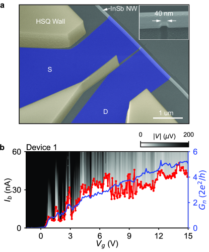
The hybrid nanowire JJs are fabricated by the recently developed shadow-wall deposition techniques 16, 18. In Fig. 1a, a scanning electron microscope (SEM) image of a representative InSb-Al nanowire JJ device is taken at a tilted angle and shown with false colors. Source (S) and drain (D) superconducting leads (blue) are formed via an in-situ angle deposition of Al film after the preparation of a clean and oxide-free InSb nanowire 19 interface (see the Methods section in the Supporting Information). Pre-patterned dielectric shadow-walls (yellow) selectively define the nanowire sections that are exposed to the Al flux during the deposition. The junction length is determined by the width of the shadow-wall in the vicinity of which the nanowire is deposited. In comparison with the etched dielectric shadow-walls used in recent works 16, 18, here we use lithographically defined shadow-walls which dimensions therefore can be as small as . This allows us to precisely control the length of nanowire JJs and to achieve surpassingly short junctions, as shown in the inset SEM image in Fig. 1a. In this work, nine nanowire JJ devices are presented (Device 1-9) with the junction length in the range of . The diameter of the nanowires is . An overview of these devices is shown in Fig. S2 in the Supporting Information.
We first characterize the nanowire Josephson junction devices by means of quantum transport at zero magnetic field and base temperature. The back side of the substrate is used as a back gate and the applied voltage acts globally on the entire nanowire. In Fig. 1b we show how the switching current (red) and the normal state conductance (blue) depend on for Device 1. In order to obtain the switching current , a four-terminal measurement is employed, where the voltage drop over the junction is measured while sweeping the current bias . is extracted from the traces as the bias value at which the junction switches to the resistive quasiparticle regime (see the Data analysis section in the Supporting Information for the extraction algorithm). The normal state conductance is obtained in the voltage-bias range - well above the double value of the induced superconducting gap of the leads (). The conductance measurements from which and are extracted are shown in Fig. LABEL:fig:SVbias and Fig. LABEL:fig:S11 and the procedure for obtaining is explained in the Data analysis section in the Supporting Information. The details on the measurement setups are given in the Measurement section in the Supporting Information. By increasing , both and , in spite of the fluctuations, become larger as the carrier states in the junction get populated and more subbands contribute to transport. At , and reach up to () and , respectively. The remaining nanowire JJs (Device 2-9) show comparable zero-field properties, as shown in Fig. LABEL:fig:SVbias and Fig. LABEL:fig:S2 in the Supporting Information. The high tunability of as well as of enables the systematic investigation of the junctions in different electro-chemical potential regimes.
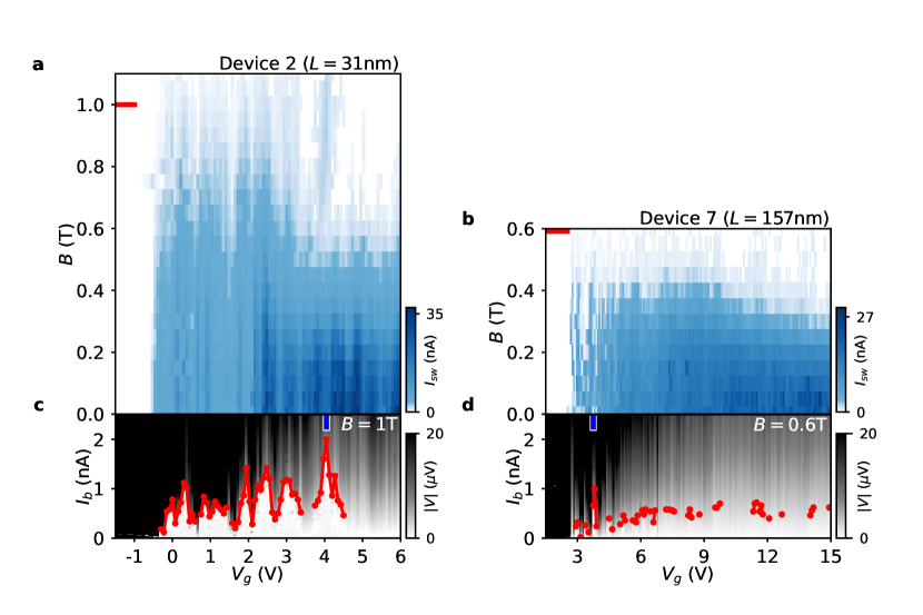
Hybrid nanowire JJs have been shown to exhibit a supercurrent evolution in a parallel magnetic field- that is strongly affected by the electro-chemical potential of the semiconducting junction 17. Therefore, when exploring the resilience of switching current in a parallel -field, the electro-chemical potential of a junction has to be taken into account. In the following, the switching current dependence on the back gate voltage and the parallel -field is studied for two JJ devices with significantly different lengths. In Fig. 2a and 2b, we show how the switching current evolves with and for Device 2 () and Device 7 (), respectively. is extracted from the corresponding traces taken at each setting of and . As shown in Fig. 2a, the short device shows a remarkable supercurrent resilience with the supercurrent persisting above a parallel field of . A linecut at (red bar) is taken and the corresponding data is shown in Fig. 2c. The switching current (red trace) continuously persists over a interval of . As a comparison, drops more rapidly with magnetic field in the long device, as shown in Fig. 2b. Fig. 2d shows that at the supercurrent is barely detectable. Besides this apparent difference, the switching current behaviours in Fig. 2a and 2b still show some similarities. Namely, of both devices manifests a better resilience against the magnetic field in an intermediate gate interval between the pinch-off and the fully open regime - interval for the short device and interval for the long device (see Fig. S5 in the Supporting Information). For the gate voltage above these intervals vanishes more rapidly in a magnetic field in both devices. Such behavior at large positive could be explained by a destructive supercurrent interference between multiple modes 17 in the open regime. Another explanation could be a reduced semiconductor-superconductor hybridization due to the gate being global and setting a large positive voltage under the superconducting leads 20, 21. This point is addressed in the discussion part following Fig. 4. An ubiquitous feature in Fig. 2a and 2b is that, as the magnetic field is increased, certain intervals in the intermediate gate regime support more resilient supercurrent. In these intervals we define the “resilient gate settings ” (blue markers in Fig. 2c and 2d) and the supercurrent at such gate settings is examined for all devices in the following paragraph.
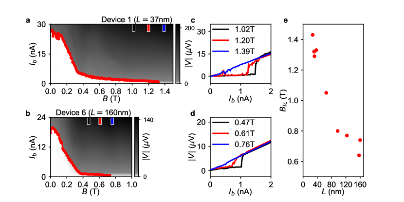
In Fig. 3 we focus on the supercurrent at the resilient gate settings . For Device 1-7 we determine the values as shown and described in Fig. S6, while for Device 8-9 we choose (see the Data selection and reproducibility section in the Supporting Information). Fig. 3a shows the voltage drop over the junction as a function of the current bias and the parallel magnetic field for Device 1 (). The red dotted line marks the extracted switching current at different -fields. Three linecuts (black, red and blue) are shown in Fig. 3c - demonstrating more than supercurrent at the parallel field of . Fig. 3b and Fig. 3d show the results for Device 6 () obtained at its setting. From the overlaid red trace it can be seen that the supercurrent vanishes at , as confirmed by the linecuts shown in Fig. 3d. Analogous measurements of the switching current evolution with parallel field are carried out for all nine devices (see Fig. S7 in the Supporting Information). Finally, these dependences allow for the extraction of the maximal critical parallel magnetic field of switching current for each Device 1-9. The details of the extraction are given in the Data analysis section in the Supporting Information. By plotting versus the junction length in Fig. 3e, it can be seen how the junction length influences the measured critical field of the supercurrent. We reproducibly reach the critical fields of in the sub- junctions while drops gradually to in the longest junctions.
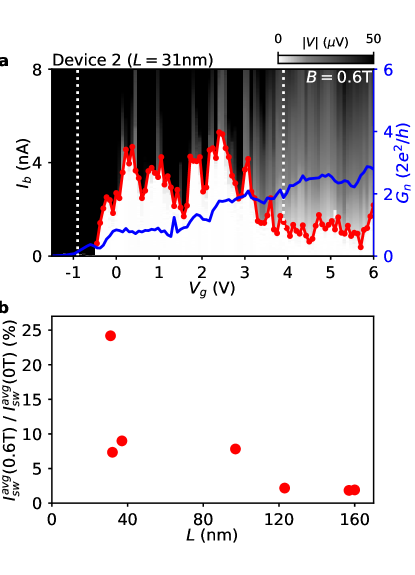
As a next step, we evaluate the supercurrent resilience over a broader gate interval - in a range of the electro-chemical potential. As our nanowire JJs are highly tunable, in Fig. 4 their supercurrent resilience against the parallel magnetic field is studied over the gate ranges in which the junctions are in the few mode regimes. Fig. 4a shows the voltage drop as a function of the current bias and the gate voltage at the parallel field of for Device 2 (), together with the switching current (red trace) and the normal state conductance (blue trace). To quantify the supercurrent resilience, the switching current in Fig. 4a is averaged in the range corresponding to (denoted by the two white dotted vertical lines) and the obtained average switching current is . An analogous averaging is done for the dependence measured at zero field and the obtained average switching current at zero field is (see Fig. S4 for the zero-field dependence and the average value). By calculating the ratio , it can be inferred that the junction of Device 2 preserves on average of its zero field switching current when the parallel field of is applied. The identical procedures of calculating the average switching currents and the ratios are carried out for Device 1-7 (see Fig. S4 and Fig. S8 in the Supporting Information). The dependence of the on the junction length is shown in Fig. 4b. It can be noticed that at finite parallel field the shorter junctions preserve larger fractions of the corresponding zero field supercurrent in the described conductance ranges. Moreover, only negligible fractions of switching current (less than ) systematically remain in the longer junctions - emphasizing their poor performance when the supercurrent resilience in tunable junctions is of interest. In comparison with Fig. 3e, the less strong dependence on the junction length can be seen in Fig. 4b. This can be attributed to particular device-specific shapes of the switching current and the normal state conductance dependences on the gate voltage. We emphasize that the particular shape of the dependence in Fig. 4b could also vary depending on the choice of the normal conductance tunability range and the subsequently determined gate intervals for averaging. However, the main qualitative features of such dependence would still remain (see Fig. S8 in the Supporting Information).
In Fig. 3 and Fig. 4 two different approaches have been taken when quantifying the supercurrent resilience against magnetic field. Both approaches have led to the same observation - by reducing the junction length supercurrent resilience against magnetic field can be significantly improved. This is a common and reproducible feature of the short JJs in our study. It is observed despite variations in the switching current dependences on the gate voltage or the parallel field (see Fig. S7 and Fig. S8). In order to better understand the interplay between the junction length and the applied gate voltage in determining the supercurrent resilience, we perform two additional measurements that are in detail discussed in the sections describing Fig. S9 and Fig. S10 in the Supporting Information. In the following three paragraphs these measurements are shortly summarized and possible origins of the reported supercurrent resilience in the short JJs are considered at the mesoscopic level.
Induced superconducting gaps for all nanowire devices and their dependence on the parallel field are studied in Fig. S9 and the corresponding section in the Supporting Information. We find that the measured induced gaps at zero field and the parallel field at which the induced gaps close are influenced not only by the back-gate voltage but by the junction length as well. This is in accordance with the known phenomenon that the proximity effect in nanowire hybrids can be controlled by the electric field 22, 23, 20, 21 - that is influenced by both the gate setting and the device geometry. The measurements in Fig. S9 show that reducing the junction length of a hybrid nanowire JJ enhances the proximity effect inside the junction. Consequently, the resilient supercurrent in the short junctions could be attributed to the enhancement of the proximity effect. Possible origins of such enhancement are discussed in more detail in the corresponding section in the Supporting Information.
Measurements on an additional short JJ device (Device 10, ) are shown in Fig. S10 and are discussed in the corresponding section in the Supporting Information. This device utilizes a bottom gate under the junction and one bottom gate under each superconducting lead. The supercurrent exhibits a nonmonotonic dependence on each of the three bottom gates especially in finite fields. This suggests that the electro-chemical potentials under the superconducting leads and in the junction form a three-dimensional parameter space in which supercurrent is defined. The back gate sweeps in our study correspond to single linecuts in this space and the supercurrent at the resilient gate settings of the back gate may not be the most resilient in the entire parameter space. Importantly, we find in Fig. S10 that applying a positive gate voltage locally under a single superconducting lead does not reduce the superconductor-semiconductor coupling to an extent that systematically limits the resilience of supercurrent.
Multimode interference is an additional mechanism that could cause the prominent supercurrent dependence on the gate voltage and magnetic field - resulting in the observation of resilient gate settings. Differences between the accumulated phases of different transversal nanowire modes increase with the junction length and the flux applied through the conductive cross-section of a junction 24. Therefore, destructive supercurrent interference due to large accumulated phase differences could be causing poor supercurrent resilience in long junctions and in open regime in all the junctions - where the conductive section increases due to high positive back gate. Furthermore, in the previous study 17 the scattering on disorder was shown to enhance multimode interference. With assuming comparable linear densities of disorder in the junctions in our study, the scattering on disorder would be more prominent in longer junctions and could therefore additionally diminish their supercurrent resilience.
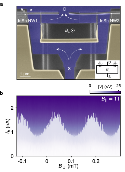
From the above results, we find that significantly reducing the nanowire JJ length is essential for preserving supercurrents in a high parallel magnetic field. Here, we take a step further and incorporate remarkably short nanowire JJs into the SQUID architecture. Fig. 5a shows a false-colored SEM of a SQUID consisting of two long hybrid JJs formed in two parallel InSb nanowires. The shadow-wall structure (yellow) is lithographically defined such that after the Al (blue) deposition two JJs enclose the superconducting loop denoted by the white arrows. Since the two arms are parallel, a magnetic field can be applied parallel to both JJs while the out-of-plane perpendicular magnetic field is applied to sweep the flux threading the SQUID loop. Upon applying , both junctions are independently tuned by the underlying local bottom gates to a finite supercurrent. As shown in Fig. 5b, the oscillations of the switching current indicate a supercurrent interference persisting despite the high parallel field being applied. In comparison with the previous work on nanowire SQUIDs 25, 2, this observation of supercurrent interference at represents a significant improvement of the SQUID field compatibility. The control and the detection of the phase of supercurrent at high magnetic field is of crucial importance for studying various high field related phenomena in hybrid nanowire devices 26, 8, 27.
In conclusion, we demonstrate that the length of a hybrid nanowire Josephson junction is an essential parameter that determines its supercurrent resilience against magnetic fields. Nanowire JJs with a length of less than can be precisely defined by the shadow-wall angle-deposition technique and are shown to reproducibly preserve supercurrent at parallel magnetic fields exceeding . Superconducting quantum interference device (SQUID) utilizing such junctions displays supercurrent interference at the parallel field of . Our study shows that hybrid nanowire Josephson junctions of significantly reduced junction length can be considered as necessary building blocks in various hybrid nanowire devices which exploit Josephson coupling at high magnetic field.
1 Author contributions
J.-Y.W. and V.L. concieved the experiment. J.-Y.W., S.H., G.P.M., N.v.L. and F.B. contributed to the substrate fabrication and/or conducted the superconductor growth. G.B, S.G. and E.P.A.M.B. grew the semiconducting nanowires. V.L. and J.-Y.W. performed the transport measurements. V.L. performed the data analysis. J.-Y.W. and L.P.K. supervised the project. V.L. and J.-Y.W. wrote the manuscript with inputs from all the other authors.
2 Acknowledgements
The authors thank Chun-Xiao Liu, Michael Wimmer and Anton R. Akhmerov for fruitful discussions. The authors are grateful to Olaf Benningshof and Jason Mensingh for important technical support. This work was financially supported by the Dutch Organization for Scientific Research (NWO), the Foundation for Fundamental Research on Matter (FOM) and Microsoft Corporation Station Q.
3 Conflict of interests
The authors declare no conflicts of interest.
References
- Yokoyama et al. 2014 Yokoyama, T.; Eto, M.; Nazarov, Y. V. Anomalous Josephson effect induced by spin-orbit interaction and Zeeman effect in semiconductor nanowires. Phys. Rev. B 2014, 89, 195407
- Szombati et al. 2016 Szombati, D. B.; Nadj-Perge, S.; Car, D.; Plissard, S. R.; Bakkers, E. P. A. M.; Kouwenhoven, L. P. Josephson -junction in nanowire quantum dots. Nature Phys. 2016, 12, 568–572
- Strambini et al. 2020 Strambini, E.; Iorio, A.; Durante, O.; Citro, R.; Sanz-Fernández, C.; Guarcello, C.; Tokatly, I. V.; Braggio, A.; Rocci, M.; Ligato, N.; Zannier, V.; Sorba, L.; Bergeret, F. S.; Giazotto, F. A Josephson phase battery. Nat. Nanotechnol. 2020, 15, 656–660
- San-Jose et al. 2014 San-Jose, P.; Prada, E.; Aguado, R. Mapping the topological phase diagram of multiband semiconductors with supercurrents. Phys. Rev. Lett. 2014, 112, 137001
- Lutchyn et al. 2010 Lutchyn, R. M.; Sau, J. D.; Sarma, S. D. Majorana fermions and a topological phase transition in semiconductor-superconductor heterostructures. Phys. Rev. Lett. 2010, 105, 077001
- Oreg et al. 2010 Oreg, Y.; Refael, G.; von Oppen, F. Helical liquids and Majorana bound states in quantum wires. Phys. Rev. Lett. 2010, 105, 177002
- Schrade et al. 2017 Schrade, C.; Hoffman, S.; Loss, D. Detecting topological superconductivity with -Josephson junctions. Phys. Rev. B 2017, 95, 195421
- Schrade and Fu 2018 Schrade, C.; Fu, L. Majorana Superconducting Qubit. Phys. Rev. Lett. 2018, 121, 267002
- Chen et al. 2018 Chen, C.-Z.; He, J. J.; Ali, M. N.; Lee, G.-H.; Fong, K. C.; Law, K. T. Asymmetric Josephson effect in inversion symmetry breaking topological materials. Phys. Rev. B 2018, 075430, 98
- Turini et al. 2022 Turini, B.; Salimian, S.; Carrega, M.; Iorio, A.; Strambini, E.; Giazotto, F.; Zannier, V.; Sorba, L.; Heun, S. Josephson diode effect in high mobility InSb nanoflags. arXiv:2207.0877 2022,
- Wu et al. 2022 Wu, H.; Wang, Y.; Xu, Y.; Sivakumar, P. K.; Pasco, C.; Filippozzi, U.; Parkin, S. S. P.; Zeng, Y.-J.; McQueen, T.; Ali, M. N. The field-free Josephson diode in a van der Waals heterostructure. Nature 2022, 604, 653–656
- Gül et al. 2017 Gül, Ö. et al. Hard superconducting gap in InSb nanowires. Nano Lett. 2017, 17, 2690–2696
- Kanne et al. 2021 Kanne, T.; Marnauza, M.; Olsteins, D.; Carrad, D. J.; Sestoft, J. E.; de Bruijckere, J.; Zeng, L.; Johnson, E.; Olsson, E.; Grove-Rasmussen, K.; Nygård, J. Epitaxial Pb on InAs nanowires for quantum devices. Nat. Nanotechnol. 2021, 16, 776–781
- Pendharkar et al. 2021 Pendharkar, M. et al. Parity-preserving and magnetic field–resilient superconductivity in InSb nanowires with Sn shells. Science 2021, 372, 508–511
- Mazur et al. 2022 Mazur, G. P. et al. Spin-mixing enhanced proximity effect in aluminum-based superconductor–semiconductor hybrids. Adv. Mater. 2022, 34, 1–8
- Heedt et al. 2021 Heedt, S. et al. Shadow-wall lithography of ballistic superconductor–semiconductor quantum devices. Nat. Commun. 2021, 12, 4914
- Zuo et al. 2017 Zuo, K.; Mourik, V.; Szombati, D. B.; Nijholt, B.; van Woerkom, D. J.; Geresdi, A.; Chen, J.; Ostroukh, V. P.; Akhmerov, A. R.; Plissard, S. R.; Car, D.; Bakkers, E. P. A. M.; Pikulin, D. I.; Kouwenhoven, L. P.; Frolov, S. M. Supercurrent interference in few-mode nanowire Josephson junctions. Phys. Rev. Lett. 2017, 119, 187704
- Borsoi et al. 2021 Borsoi, F. et al. Single-shot fabrication of semiconducting–superconducting nanowire devices. Adv. Func. Mater. 2021, p. 2102388
- Badawy et al. 2019 Badawy, G.; Gazibegovic, S.; Borsoi, F.; Heedt, S.; Wang, C.-A.; Koelling, S.; Verheijen, M. A.; Kouwenhoven, L. P.; Bakkers, E. P. A. M. High mobility stemless InSb nanowires. Nano Lett. 2019, 19, 3575–3582
- de Moor et al. 2018 de Moor, M. W. A. et al. Electric field tunable superconductor-semiconductor coupling in Majorana nanowires. New J. Phys. 2018, 20, 103049
- Shen et al. 2021 Shen, J. et al. Full parity phase diagram of a proximitized nanowire island. Phys. Rev. B 2021, 104, 045422
- Mikkelsen et al. 2018 Mikkelsen, A. E.; Kotetes, P.; Krogstrup, P.; Flensberg, K. Hybridization at superconductor-semiconductor interfaces. Phys. Rev. X 2018, 8, 031040
- Antipov et al. 2018 Antipov, A. E.; Bargerbos, A.; Winkler, G. W.; Bauer, B.; Rossi, E.; Lutchyn, R. M. Effects of gate-induced electric fields on semiconductor Majorana nanowires. Phys. Rev. X 2018, 8, 031041
- Gharavi and Baugh 2015 Gharavi, K.; Baugh, J. Orbital Josephson interference in a nanowire proximity-effect junction. Phys. Rev. B 2015, 91, 245436
- Wang et al. 2022 Wang, J.-Y. et al. Supercurrent parity meter in a nanowire Cooper pair transistor. Sci. Adv. 2022, eabm9896
- Liu et al. 2021 Liu, C.-X.; van Heck, B.; Wimmer, M. Josephson current via an isolated Majorana zero mode. Phys. Rev. B 2021, 103, 014510
- Schrade and Fu 2018 Schrade, C.; Fu, L. Parity-controlled Josephson effect mediated by Majorana Kramers pairs. Phys. Rev. Lett. 2018, 120, 267002