Design of Spintronics-based Neuronal and Synaptic Devices for Spiking Neural Network Circuits
(Invited Paper)
Abstract
Topologically stable magnetic skyrmion has a much lower depinning current density that may be useful for memory as well as neuromorphic computing. However, skyrmion-based devices suffer from the Magnus force originating from the skyrmion Hall effect, which may result in unwanted skyrmion annihilation if the magnitude of the driving current gets too large. A design of an artificial neuron and a synapse using a synthetic antiferromagnetically coupled bilayer device, which nullifies the Magnus force, is demonstrated in this work. The leak term in the artificial leaky integrate-and-fire neuron is achieved by engineering the uniaxial anisotropy profile of the neuronal device. The synaptic device has a similar structure as the neuronal device but has a constant uniaxial anisotropy. The synaptic device also has a linear and symmetric weight update, which is a highly desirable trait of an artificial synapse. Neuronal and synaptic devices based on magnetic domain-wall (DW) motion are also studied and compared to skyrmionic devices. Our simulation results show the energy required to perform such operation in DW or skyrmion-based devices is on the order of a few fJ.
Index Terms:
spiking neuron, synapse, magnetic domain wall, magnetic skyrmionI Introduction
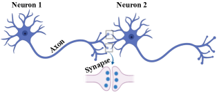
Brain-inspired neuromorphic computing has emerged as one of the promising approaches that can perform cognitive tasks [1, 2] with human-like accuracy. Neurons and synapses are the two key components in a biological spiking neural network (SNN) in which billions of neurons are interconnected via trillions of synapses. Information in an SNN propagates in the form of a spike that is transmitted from one neuron (pre-neuron) to the next neuron (post-neuron) connected via a synapse—the spikes get modified by the synaptic weight during this process. The schematic of a simple SNN consisting of two neurons that are connected by synapses is shown in Fig. 1. When the pre-neuron (Neuron1) fires a spike, the synapse modifies the spike with its synaptic weight before forwarding it to the post-neuron (Neuron2).
Among various emerging devices (e.g., resistive memory [3, 4] and phase-change memory [5, 6]), spintronics [7, 8, 9, 10] is arguably the most promising technology due to its non-volatile nature, low power consumption, ultrafast dynamics, higher endurance, and stochastic nature [11, 12, 13]. Magnetic domain wall (DW) [14, 15] and skyrmion-based devices [16, 17] are the most popular among various other spintronics devices. Among these two, skyrmion-based devices are promising due to their topological stability (implies robustness against defects) and lower depinning current density (implies lower power consumption) compared to magnetic domain wall-based devices. However, skyrmion-based devices have limitations due to the Magnus force [18, 19], which acts perpendicular to the direction of the injected current. Consequently, the skyrmion moves along a resultant direction determined by spin-torque due to injection current and the Magnus force. The magnitude of the Magnus force is directly proportional to the velocity of the skyrmion, which is proportional to the magnitude of the injected current density. If the magnitude of the injected spin current is too large, the Magnus force may be large enough to annihilate the skyrmion at the nanotrack edge during its motion, which limits the utility of skyrmions for high-speed applications.
To drive the DW/skyrmion in a nanotrack, a spin current is needed, which can be injected either by (i) current-in-plane (CIP) or (ii) current-perpendicular-to-plane (CPP) scheme. CPP scheme stands out to be more energy efficient compared to CIP, due to the lower current density needed to drive the DW/skyrmion. Elimination of the Magnus force in a skyrmion-based device was demonstrated using the CIP scheme in Ref. [20], through micromagnetic simulation, with the condition that the non-adiabatic spin-transfer-torque factor, , needs to be exactly equal to the Gilbert damping constant, . Hence, this method is sensitive to the material parameter and any mismatch can introduce the undesired Magnus force.
Alternatively, a bilayer device where the magnetization of two ferromagnet (FM) layers are coupled via an antiferromagnetically (AFM) exchange coupling may be promising for eliminating the Magnus force. The Magnus force can be completely nullified if the coupling constant between the magnetic layers is sufficiently large [21]. In this work, we use micromagnetic simulations to demonstrate how this bilayer device can be designed to be neuronal and synaptic devices. The design of neuronal and synaptic devices using DW motion in a traditional monolayer structure is also presented and compared with the skyrmionic device.
II Device structure
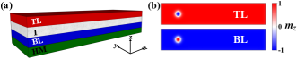
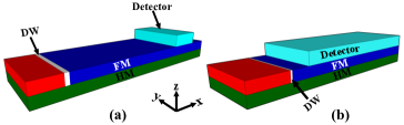
The bilayer system consists of a heavy metal (HM)/FM/insulator (I)/FM stack shown in Fig. 2(a). The FM layer adjacent to HM is the bottom layer (BL) whereas the topmost FM layer is the top layer (TL). Due to the spin-Hall effect, charge current injected through the HM layer generates a spin-current that is spin-polarized along the -direction and flows in the -direction into the BL to drive the motion of any DW or skyrmion in it. The HM layer also gives rise to the Dzyaloshinskii-Moriya interaction (DMI) that stabilizes the skyrmion in the device. Both TL and BL are designed with perpendicular magnetic anisotropy (PMA) and their magnetizations are coupled by AFM exchange interaction. In the following, the initial magnetizations of TL and BL are assumed to be along + and - direction, respectively.
Assume the size of both TL and BL layers in Fig. 2(a) is 260 nm50 nm1 nm in the following discussion. The membrane potential in the leaky integrate-and-fire (LIF) neuron device implemented using the bilayer structure in Fig. 2(a) is represented by the position of a skyrmion-pair along the length of the device. Local injection of a 5 current pulse that is spin-polarized along the --direction can nucleate a skyrmion at the desired location of TL. The magnetization of the core of the nucleated skyrmion points in the --direction. As shown in Fig. 2(b), another skyrmion with opposite magnetization to that in TL is simultaneously nucleated in BL simultaneously due to the AFM coupling. Input spikes that are integrated by the device are in the form of current pulses that are injected along the length of the device, which moves the skyrmion-pair.
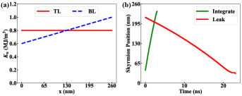
The leak term in the neuron device may be achieved by implementing a gradient in the uniaxial anisotropy constant, , along the length of the BL. On the other hand, the TL has a uniform as shown in Fig. 3(a). To validate the integration and leak functionalities, we test the device in the following way. A skyrmion-pair in the TL and BL is initially nucleated at =50 nm. A uniform 30 charge current density is next applied in the HM along the +-direction, which moves the skyrmions in TL and BL in unison. The position of the skyrmion center in the TL versus time is plotted as the green curve in Fig. 3(b). The skyrmion in the BL has the same behavior due to the AFM coupling. Thus, the position of the skyrmion appears as the time-integral of the injected current and the integration functionality of the proposed neuron device is verified.
Next, consider when the skyrmion-pair is initially at =215 nm and no charge current flows through the device. Notice that, as shown by the red color plot in Fig. 3(b), the skyrmion in BL moves gradually along the --direction due to the gradient. Due to AFM coupling, the skyrmion in TL moves in unison with that in BL. After 23 ns, the skyrmion stops at =25 nm due to the edge repulsion. This behavior of the skyrmion resembles the leak functionality of neuron.
On the other hand, synaptic devices should behave like a non-volatile memory devices. This can be achieved in the same bilayer device as the neuron if the is uniform along the device in both TL and BL. The synapse emulates different weight values to modulate the signal transmission from the pre-neuron to the post-neuron. Multiple values of the synaptic weight is achieved in a device having multiple conductance levels. These conductance levels can be achieved using multiple skyrmions in the device. With the application of different current pulses, the skyrmions can be moved between the two sides of the device, which changes the conductance of the detector arising from the magnetoresistance effect.
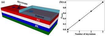
To demonstrate this, consider if three skyrmions are initially on the left half of a bilayer device and the detector is placed on the other half as can be seen from Fig. 4(a). When current pulses are applied, these skyrmions enter the detector area one by one, which changes the conductance of that area. The variation of the conductance in normalized scale, denoted by , with the number of skyrmions under the detector area is plotted in Fig. 4(b) that shows a linear relationship. Thus, the number of skyrmions under the detector area may be used to represent different weight values in the synapse to modulate the neuronal spikes.
II-A Domain-wall (DW) based devices
Magnetic DW based devices do not suffer from the Magnus force issue and thus, a conventional monolayer structure may be used to implement these neuronal and synaptic devices. Consider the structure shown in Fig. 5, which consists of a single FM layer with PMA and is attached to a HM layer. In the neuron device, the membrane potential is represented by the position of the DW shown by the white region between red (magnetized along +) and blue (magnetized along -) regions. A gradient is engineered into the FM layer to implement the leak behavior of the neuron. To make the synaptic device, a long detector along the length of the device as shown in Fig. 5(b) is required. The operation principle of the DW-based devices is similar to their skyrmionic counterparts in that the forward (backward) movement of the DW under the detector would increase (decrease) the conductance of the detector.
III Results and Discussion
Magnetization dynamics in FM layers is simulated in the Object Oriented MicroMagnetic Framework (OOMMF) [22] with the DMI extension module [23]. In all our simulations, the simulation volume is discretized into 2 nm2 nm1 nm cells. The material parameters assumed are those for system [16, 21].
III-A Demonstration of neuron device
The integration and leak functionality of a bilayer-based skyrmionic neuron device has already been described in Section I. Here, the performance of the skyrmion and domain wall-based neuron devices are explained.
First, consider the skyrmion-based neuron device. The membrane potential of the neuron is represented by the position of the skyrmion core in TL. The firing of the neuron occurs when the skyrmion reaches near the right end of the device, which may be sensed by a change of the local magnetoresistance measured using a detector based on the magnetic tunnel junction (MTJ). To achieve the leaky behavior, a gradient described by where =1.538 , =0.6 , and is the position along the length of the nanotrack, is engineered into BL. The of TL is at a constant value along its length.
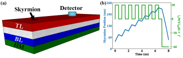
Now, consider that the skyrmion was nucleated at =40 nm and the detector is placed at =230 nm, as shown by the schematic in Fig. 6(a). A square current density pulse (30 ) having 0.5 ns pulse width and 1 ns period is applied along the +-direction to drive the skyrmion as shown by the green color plot in Fig. 6(b). During the high state of the applied pulse, the skyrmion moves in the +-direction. During the low state, the skyrmion moves in the --direction due to the gradient. The motion of the skyrmion is demonstrated by the blue graph of the skyrmion position versus time in Fig. 6(b). Once the skyrmion reaches under the detector (at 7 ns), the neuron fires and a reset circuitry (not shown) is triggered to activate a reset 60 current pulse that resets the skyrmion to its initial position. This reset pulse is applied for 1 ns, shown in Fig. 6(a), which moves the skyrmion along --direction as shown in Fig. 6(b) (between 7 ns and 8 ns). The energy consumption to move the skyrmions in the nanotrack may be calculated as,
| (1) |
where is the resistivity of the HM [24]. , , , and are the length (along the -axis), cross-sectional area (in the -plane) of the HM layer, current density, and time delay to move the skyrmion. The energy required for the rest-to-fire-to-reset operation of this neuron is 8.775 fJ.
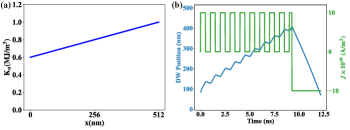
Next, consider the neuron operation in a DW-based device shown in Fig. 5(a). Unlike the skyrmion-based device, the lateral dimension of the DW-based neuron device is 512 nm32 nm and the thickness of the FM layer is 1 nm. A similar gradient along the length of the device as shown in Fig. 7(a) is engineered into the FM to achieve the leak functionality. For driving the DW, a square charge current pulse (10) with a period of 1 ns and pulse-width of 0.5 ns is injected into the HM as shown by the green plot in Fig. 7(a). Similar to the skyrmion device, the DW also moves along the +-direction during a high state of the injected pulse and moves backward during the low state due to the gradient. The variation of DW position versus time is shown by the blue plot in Fig. 7(b). When the DW crosses 420 nm, the conductance state of the detector reaches a maximum, which leads to the firing of the neuron. Our simulation results show that it takes 9.26 ns for the DW to go from its initial position to the firing position in the detector. A reset circuitry is needed to generate a current pulse to return the DW back to its initial position. For reset, the magnitude of is also 10 and it takes 2.92 ns to complete the reset process. A total of 1.25 fJ energy is consumed to complete the rest-to-fire-reset process (0.779 fJ for the firing process and 0.471 fJ for the reset process).
III-B Demonstration of synapse device
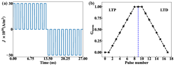
For the skyrmion-based synapse device, consider a bilayer device shown in Fig. 4(a) with lateral dimensions of 1000 nm50 nm, and the thicknesses of both TL and BL layers are 1 nm. As there is no need for the leaky behavior, both TL and BL have a constant value of 0.8 . The TL nanotrack is further divided into two equal halves, where seven skyrmions are nucleated at equidistant on the left half. An MTJ-like detector is on the right half, we place an MTJ like a detector. The operation of the synaptic device is validated by applying a train of the square current pulse into the HM. The magnitude of the current pulse is 30, with a time-period of 1.5 ns and pulse width 0.75 ns.
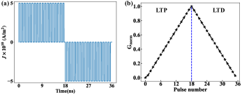
The long term potentiation (LTP) operation is achieved by injecting the square current pulses in +-direction whereas the long term depression (LTD) is achieved by reversing the direction of current flow. The applied current density () for the LTP and LTD operation is shown in Fig. 8(a). Individual pulse applied during the LTP operation moves the skyrmions one-by-one from the left half into the detector placed at the right half of the device. As the skyrmions move into the detector area, the conductance of the detector starts to increase which is shown in Fig. 8(b) by the plot of the normalized conductance, of the detector versus the number of pulses applied during the LTP operation. The eight discrete values marked by black asterisks in Fig. 8(b) present the possible synaptic weight for the modulation of the neuron spikes. These eight weights represent different conductance values since the number of skyrmions in the detector area can vary from 0 to 7. When all seven skyrmions are in the detector area, the weight/conductance attains a maximum value of 1 (normalized scale). Further pulse current does not increase the conductance as can be seen from the same value at pulse number 9 and 10 in Fig. 8(b).
During the LTD operation, the skyrmions in the detector area go back to the left half one-by-one in a similar fashion, which reduces the conductance of the detector area as can be seen from Fig. 8(b). Our simulation results show a total of 6 ns is required to complete the entire LTP or LTD operation. This generates highly linear and symmetric weight update characteristics (Fig. 8(b)), which is a highly desirable condition for an artificial synapse. Using Eq. (1), the energy required to fully change the synaptic weights of our proposed device from minimum to maximum is 27 fJ. Since there are a total of seven skyrmions in TL, the average energy required to adjust the synaptic weight is 3.587 fJ/unit.
Now consider the DW-based synaptic device shown in Fig. 5(b). Like the previous DW-based neuron device, the lateral size of the synaptic device is 512 nm32 nm, and the thickness of the FM layer is 1 nm. Unlike, the skyrmion-based synapse device, the detector spans from =40 nm to the rest of the device along its length. A square current density pulse train with time-period, pulse width, and magnitude of 1 ns, 0.5 ns, and 5, respectively, is injected into HM. The current is injected for the first 18 ns along the +-direction to perform the LTP operation and then in the reverse direction for another 18 ns for the LTD operation. The variation of the injected current density with time for the entire operation is plotted in Fig. 9(a). The initial position of the DW is just outside the detector area. With the injection of the current pulses during LTP, DW starts to move in the +-direction. As the DW enters the detector area and moves farther in, the conductance of the detector increases as seen in the graph of the normalized conductance, , versus the current pulse number in Fig. 9(b). During LTD, the DW moves in the opposite direction and thus, the conductance of the detector starts to decrease as can be seen from Fig. 9(b). The results in Fig. 9(b) show that the weight update during LTP and LTD, is linear in nature and also highly symmetric. A total of 19 unique conductance states is achieved by different DW positions driven by the injected current. The energy consumed to fully change the synaptic weights of this device from minimum to maximum is 0.36 fJ, which translates to an average of 0.02 fJ/unit.
| Technology | Device | Lateral Dimension | Net Energy |
| Skyrmion | Neuron | 26050 | 8.775 fJ |
| Synapse | 100050 | 27 fJ | |
| DW | Neuron | 51232 | 1.25 fJ |
| Synapse | 51232 | 0.36 fJ |
A comparison of the neuron and synapse devices studied in this work is shown in Table I. These results show that DW-based device has advantages in lower energy consumption and the same device geometry may be used as a neuron and synapse with just a modification in the profile. The lower energy consumption is because the current needed to drive the DW motion is 10% of that needed in the skyrmionic devices. Both the skyrmionic and DW-based synapses produce highly symmetrical and linear weight update characteristics, which is one of the key requirements for an artificial synapse. However, the number of conductance states is higher in the DW-based synaptic device as compared to its skyrmionic counterpart, in which the number of conducting states depends on the number of available skyrmions. It can be anticipated that the DW-based synapse emulates SNNs with 4-bit weights, which can lead to improved inference accuracy as compared to 3-bit weights in the skyrmionic synapse. Also, due to the active repulsion force between the skyrmions, a longer device is required to accommodate the large number of skyrmions needed for the number of conducting states.
IV Conclusions
In summary, spintronics neuron and synapse device concepts using skyrmion and DW were investigated. For the neuron devices, the membrane potential is represented by the position of the skyrmion or the DW, whereas the synaptic weight is determined by the number of conductance states in a detector area of the synapse device. Between DW and skyrmion devices, DW-based devices seem more advantageous as it consumes 86% and 97% less energy for the neuron and synapse devices respectively. These impressive advantages in energy consumption stem from the 9 larger current needed for skyrmion motion as compared to DW motion.
References
- [1] D. Marković, A. Mizrahi, D. Querlioz, and J. Grollier, “Physics for neuromorphic computing,” Nature Reviews Physics, vol. 2, no. 9, pp. 499–510, 2020.
- [2] K. Roy, A. Jaiswal, and P. Panda, “Towards spike-based machine intelligence with neuromorphic computing,” Nature, vol. 575, no. 7784, pp. 607–617, 2019.
- [3] S. Yu, Y. Wu, R. Jeyasingh, D. Kuzum, and H.-S. P. Wong, “An electronic synapse device based on metal oxide resistive switching memory for neuromorphic computation,” IEEE Transactions on Electron Devices, vol. 58, no. 8, pp. 2729–2737, 2011.
- [4] S. Park, H. Kim, M. Choo, J. Noh, A. Sheri, S. Jung, K. Seo, J. Park, S. Kim, W. Lee et al., “Rram-based synapse for neuromorphic system with pattern recognition function,” in 2012 international electron devices meeting. IEEE, 2012, pp. 10–2.
- [5] T. Tuma, A. Pantazi, M. Le Gallo, A. Sebastian, and E. Eleftheriou, “Stochastic phase-change neurons,” Nature nanotechnology, vol. 11, no. 8, pp. 693–699, 2016.
- [6] S. Kim, M. Ishii, S. Lewis, T. Perri, M. BrightSky, W. Kim, R. Jordan, G. Burr, N. Sosa, A. Ray et al., “Nvm neuromorphic core with 64k-cell (256-by-256) phase change memory synaptic array with on-chip neuron circuits for continuous in-situ learning,” in 2015 IEEE international electron devices meeting (IEDM). IEEE, 2015, pp. 17–1.
- [7] A. Sengupta, Y. Shim, and K. Roy, “Proposal for an all-spin artificial neural network: Emulating neural and synaptic functionalities through domain wall motion in ferromagnets,” IEEE transactions on biomedical circuits and systems, vol. 10, no. 6, pp. 1152–1160, 2016.
- [8] W. H. Brigner, N. Hassan, L. Jiang-Wei, X. Hu, D. Saha, C. H. Bennett, M. J. Marinella, J. A. C. Incorvia, F. Garcia-Sanchez, and J. S. Friedman, “Shape-based magnetic domain wall drift for an artificial spintronic leaky integrate-and-fire neuron,” IEEE Transactions on Electron Devices, vol. 66, no. 11, pp. 4970–4975, 2019.
- [9] D. Zhang, L. Zeng, K. Cao, M. Wang, S. Peng, Y. Zhang, Y. Zhang, J.-O. Klein, Y. Wang, and W. Zhao, “All spin artificial neural networks based on compound spintronic synapse and neuron,” IEEE transactions on biomedical circuits and systems, vol. 10, no. 4, pp. 828–836, 2016.
- [10] M.-C. Chen, A. Sengupta, and K. Roy, “Magnetic skyrmion as a spintronic deep learning spiking neuron processor,” IEEE Transactions on Magnetics, vol. 54, no. 8, pp. 1–7, 2018.
- [11] Y. Zhang, W. Zhao, J.-O. Klein, W. Kang, D. Querlioz, Y. Zhang, D. Ravelosona, and C. Chappert, “Spintronics for low-power computing,” in 2014 Design, Automation & Test in Europe Conference & Exhibition (DATE). IEEE, 2014, pp. 1–6.
- [12] Y. Shim, S. Chen, A. Sengupta, and K. Roy, “Stochastic spin-orbit torque devices as elements for bayesian inference,” Scientific reports, vol. 7, no. 1, pp. 1–9, 2017.
- [13] D. Das and X. Fong, “A Fokker–Planck approach for modeling the stochastic phenomena in magnetic and resistive random access memory devices,” IEEE Transactions on Electron Devices, vol. 68, no. 12, pp. 6124–6131, 2021.
- [14] S. S. Parkin, M. Hayashi, and L. Thomas, “Magnetic domain-wall racetrack memory,” Science, vol. 320, no. 5873, pp. 190–194, 2008.
- [15] D. Das and X. Fong, “Self-reset schemes for magnetic domain wall-based neuron,” arXiv preprint arXiv:2210.13881, 2022.
- [16] J. Sampaio, V. Cros, S. Rohart, A. Thiaville, and A. Fert, “Nucleation, stability and current-induced motion of isolated magnetic skyrmions in nanostructures,” Nature nanotechnology, vol. 8, no. 11, pp. 839–844, 2013.
- [17] D. Das, B. Muralidharan, and A. Tulapurkar, “Skyrmion based spin-torque nano-oscillator,” Journal of Magnetism and Magnetic Materials, vol. 491, p. 165608, 2019.
- [18] N. Nagaosa and Y. Tokura, “Topological properties and dynamics of magnetic skyrmions,” Nature nanotechnology, vol. 8, no. 12, pp. 899–911, 2013.
- [19] G. Chen, “Skyrmion hall effect,” Nature Physics, vol. 13, no. 2, pp. 112–113, 2017.
- [20] S. Li, W. Kang, Y. Huang, X. Zhang, Y. Zhou, and W. Zhao, “Magnetic skyrmion-based artificial neuron device,” Nanotechnology, vol. 28, no. 31, p. 31LT01, 2017.
- [21] X. Zhang, Y. Zhou, and M. Ezawa, “Magnetic bilayer-skyrmions without skyrmion Hall effect,” Nature communications, vol. 7, no. 1, pp. 1–7, 2016.
- [22] M. J. Donahue and D. G. Porter, “OOMMF user’s guide, version 2.0a0,” 2019, http://math.nist.gov/oommf/. [Online]. Available: https://math.nist.gov/oommf/
- [23] S. Rohart and A. Thiaville, “DMExchange6Ngbr: OOMMF oxs extension modules,” 2012, https://math.nist.gov/oommf/contrib/oxsext. [Online]. Available: https://math.nist.gov/oommf/contrib/oxsext/
- [24] M.-H. Nguyen, D. Ralph, and R. Buhrman, “Spin torque study of the spin hall conductivity and spin diffusion length in platinum thin films with varying resistivity,” Physical review letters, vol. 116, no. 12, p. 126601, 2016.