Ultrafast laser welding of silicon
Abstract
While ultrafast laser welding is an appealing technique for bonding transparent workpieces, it is not applicable for joining silicon samples due to nonlinear propagation effects which dramatically diminishes the possible energy deposition at the interface. We demonstrate that these limitations can be circumvented by local absorption enhancement at the interface thanks to metallic nanolayer deposition. By combining the resulting exalted absorption with filament relocation during ultrafast laser irradiation, silicon samples can be efficiently joined. Shear joining strengths MPa are obtained for 21-nm gold nanolayers without laser-induced alteration of the transmittance. Such remarkable strength values hold promises for applications in microelectronics, optics, and astronomy.
1. Introduction
Ultrafast laser welding increasingly attracts attention as it offers the possibility to join a wide variety of materials in a fast, clean, and adhesive-free way [1]. It relies on the propagation of ultrashort laser pulses through a first workpiece, energy deposition at the interface with a second workpiece, which locally leads to melting, resolidification, and the creation of strong bonds between the two workpieces. This technique can be applied to similar and dissimilar materials [2]. However, until recently, ultrafast laser welding was limited to configurations where the first workpiece is transparent and exhibits a large band gap (e.g., glass, polymer) [3, 2, 4, 1, 5, 6, 7, 8]. In contrast, silicon as a narrow band-gap material exhibits a high nonlinear refractive index causing the formation of filaments [9, 10, 11, 12]. Consequently, in such a nonlinear propagation regime, the energy deposition is strongly limited and delocalized, which is a major hurdle when one aims at joining silicon to another material. Recently, we have demonstrated that silicon–metal ultrafast laser welding is achievable when the nonlinear focal shift is precompensated, i.e., the maximum fluence is relocated at the interface between both materials [13]. In this configuration, the free electrons of the metal linearly absorb the laser flux by inverse Bremsstrahlung. However, silicon–silicon ultrafast laser welding is still an open issue, as the absorption is necessarily nonlinear (multi-photon ionization)—and thus, the energy deposition at the interface between two silicon samples is less efficient than in the silicon–metal configuration. While it was shown that nanosecond pulses [14] or continuous light [15] can be employed for joining silicon samples, thermal effects in such regimes are expected to decrease the degree of control on the energy deposition. The demonstration of an ultrafast laser-based technique for joining stacked semiconductors such as silicon would have direct applications in microelectronics, and even beyond. For instance, this technique would have strong potential for fabricating optical components based on stacked semiconductors with applications in laser manufacturing [16], and astronomy [17].
In this paper, we demonstrate ultrafast laser welding of silicon. To optimize the energy deposition at the interface between the silicon samples, our recently developed filament relocation technique is applied [13]. Prior to the welding, the absorption at the interface is increased by the deposition of a gold nanolayer. Welding attempts without nanolayer failed, as the interface is not modified with the laser radiation. The influence of the gold nanolayer thickness on the transmittance of the joined samples and the bonding strength is evaluated. The best performance is obtained for the thinnest gold nanolayers (21 nm), which yield shear joining strengths MPa between the samples. This result originates from the high temperatures which can be reached for the thinnest nanolayers, as confirmed by the increase in the laser-induced damage threshold (LIDT) with the nanolayer thickness. Ultimately, observations of the welds after separation show that the thickest nanolayers lead to inefficient joining between the silicon samples.
2. Rationale
In order to devise a procedure for performing ultrafast laser welding of silicon, let us develop in this Section our reasoning based on the existing state of the art. First, let us recall that the only demonstrations of laser-joined silicon samples have been realized with nanosecond pulses [14] and continuous light [15]. This is consistent with the fact that this long-interaction regime is adapted to the production of repeatable modifications inside silicon [18, 19, 20, 21, 22, 23, 24]. However, the modifications produced in this regime exhibit large heat-affected zones [25], as a consequence of thermal runaway during the interaction. Such large-sized modifications are likely to severely alter the material properties, causing for instance degradation of the thermal and electrical properties, wavefront distortions, light scattering, and tilt between the samples.
In contrast, ultrashort pulses ( ps) lead to limited heat-affected zone. However, permanent modifications are extremely challenging to produce in the bulk and the exit surface of silicon with ultrashort laser pulses [12], unless complex approaches are implemented for optimizing the spatial [26, 27, 28], spectral [29, 30], or temporal [31, 32, 33] properties of the irradiation. These limitations originate from the high nonlinear refractive index of silicon (on the order of cm2 W-1 [34, 35]), which causes micro-filamentation at modest peak powers—and thus, an intensity clamping similar to that described for transparent media [36, 37]. The main difference between silicon and transparent media is that the intensity saturation level in silicon is below the damage threshold.
In the context of ultrafast laser welding, the challenge to produce permanent modifications inside silicon leads to a paradoxical situation. Traditionally, for glasses, higher bonding strengths are observed for samples kept in optical contact during the laser welding [38, 39]. However, by definition, two samples in optical contact behave optically as a single sample. For silicon, this implies that attempting to join samples in optical contact practically means to modify the bulk of a single silicon sample, which is extremely hard to achieve. On the other hand, when the silicon samples are not in optical contact, the air gap between these would result in high losses ( at each air–silicon interface) due to the large refractive index mismatch between silicon and air. Furthermore, as an excellent thermal insulator, air would hinder efficient transfer of the laser-produced heat, as well as material interpenetration from one sample to the other—and thus, the creation of strong bonds between the samples.
One way to sidestep this paradox is to engineer the exit surface so that the energy deposition is locally increased. For instance, surface grinding causes increased roughness, in turn acting as damage precursor through electric field enhancement. While this approach is suitable for surface-seeded inscription of waveguides in the bulk of silicon [40], optical contact between rough samples cannot be achieved. In order to reach the damage threshold on the exit surface of silicon, and simultaneously preserve low surface roughness, the deposition of a thin metallic film is an excellent option. Indeed, metals exhibit free electrons that are able to linearly absorb the laser flux by inverse Bremsstrahlung, which is particularly efficient for infrared wavelengths such as inevitably employed for reaching the transparency domain of silicon. This exalted absorption on the exit surface is supported by different studies. First, selective laser ablation of gold films deposited on the exit surface of silicon was shown in Refs. [41, 42]. Moreover, this approach is consistent with our recent demonstration of silicon–metal ultrafast laser welding [13].
Various metals can be considered as the absorbing layer between two silicon samples, as most of them exhibit analogous optical properties in the infrared. In our study, we selected gold as it does not oxidize, making the joined samples less prone to aging problems. Finally, one must mention the existing compromise concerning the thickness of the absorbing layer. On the one hand, an extremely thin film would result in insufficient absorption enhancement, and the silicon samples are unlikely to be joined. On the other hand, excessive film thickness would hinder the interpenetration of the silicon samples. A reasonable compromise consists of using film thicknesses on the same order of magnitude as the optical penetration depth of the metal ( nm for gold). The influence of the gold nanolayer thickness on the bonding quality is examined below.
3. Experimental arrangement
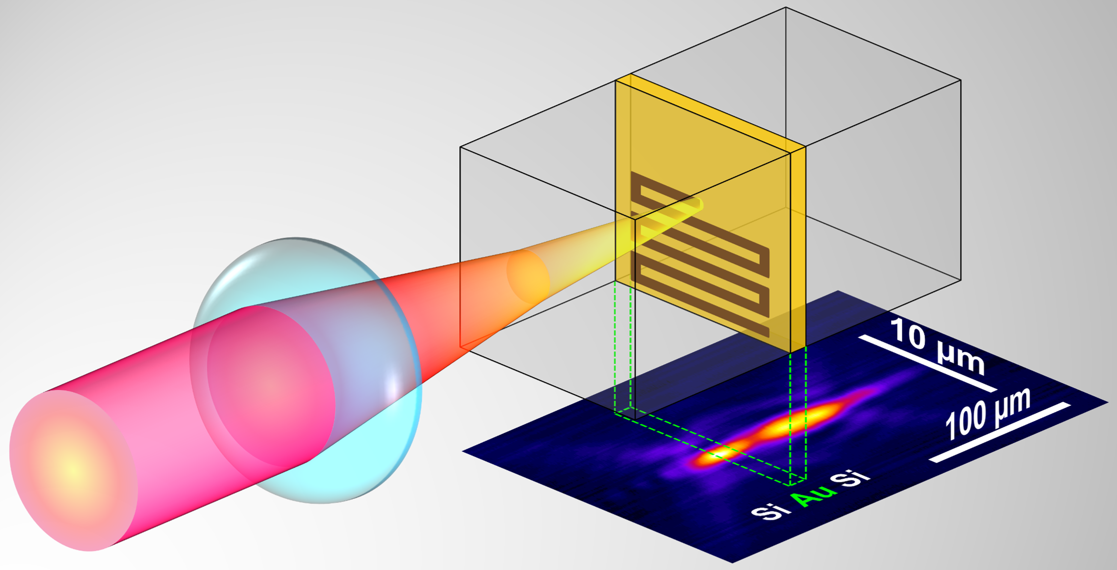
The experimental arrangement for performing silicon–silicon ultrafast laser welding is identical to that employed in the silicon–metal configuration as described in Ref. [13]. It relies on pulses at a wavelength of 1555 nm delivered at kHz repetition rate by an Er-doped fiber laser (Raydiance Inc., Smart Light 50). The pulse duration is adjusted to 9.8 ps (full width at half-maximum) to avoid excessive nonlinearities and achieve better welding than with sub-picosecond pulses [6]. For the same reasons, the pulse energy is set to 900 nJ, which corresponds to the nonlinear propagation regime where the peak fluence in the bulk of silicon saturates to 125 mJ/cm2 without catastrophic focusing and defocusing dynamics (see Section S1, Supporting Information). The beam is focused with an objective lens of numerical aperture (Mitutoyo, M Plan Apo NIR ). In the linear propagation case, the Gaussian beam diameter at the focus is m, as measured with an InGaAs camera and confirmed by simulations with the InFocus vectorial model [43, 44].
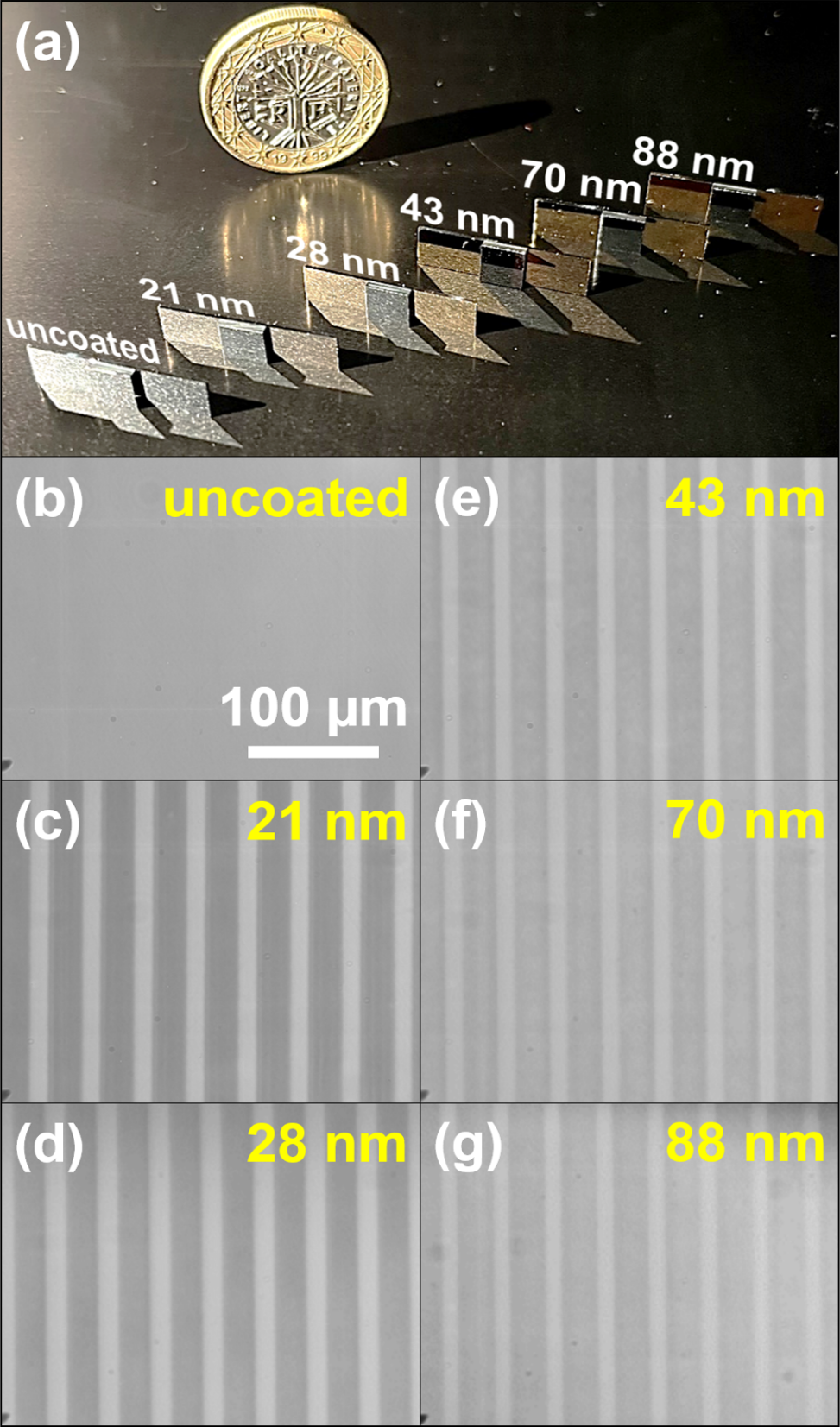
The first and second silicon samples (hereafter referred to as the “top” and “bottom” samples, respectively) are undoped, 100-oriented, double-side polished, with resistivity cm, total thickness variation m, bow m, and wrap m. The dimensions of the top and bottom sample are mm3 and mm3, respectively. A gold nanolayer is deposited on the entrance surface of the bottom sample by sputtering. The nanolayer thickness is adjusted by changing the sputtering time, and measured with a stylus profiler. Gold nanolayer thicknesses of 0 (i.e., no nanolayer), 21, 28, 43, 70, and 88 nm have been tested. For each configuration, the experiments have been performed on five sample pairs for repeatability. The laser-induced damage threshold (LIDT, in J/cm2) is evaluated for each nanolayer by applying 100,000 pulses focused on different sites with the same focusing objective lens as in the welding experiments.
During welding, the samples are maintained in optical contact by means of a clamping system described in Ref. [45], so that there is no air gap between them. The welding pattern is a raster scan at a scanning speed mm s-1, with 40-m distance between the lines, and a total scanned area of mm2. The number of pulses per point is , where m is the beam diameter at 1/e2 at the nonlinear focus (see Section S1, Supporting Information), and kHz is the laser repetition rate. A customized dark-field microscope enables us to accurately position the entrance surface of the top samples with respect to the geometrical focus. Two steps are then applied to optimize the energy deposition at the interface. First, the geometrical focus is positioned at the interface by moving it from the entrance surface of the top sample by downstream the laser, where is the refractive index of silicon at a wavelength of 1555 nm [46], and is the thickness of the top sample. In addition, we apply a second step described in Ref. [13] and illustrated in Fig. 1, which consists of filament relocation. To do so, the nonlinear focal shift is determined with nonlinear propagation imaging. For the input pulse energy used in the welding experiments (900 nJ, corresponding to an input peak power kW), m, which is precompensated by moving the objective lens downstream the laser by . These two steps ensure that the fluence at the interface is optimized.
Ex-situ characterization of the welds is performed by various means listed below.
-
•
A customized infrared transmission microscope is used for inspecting the interface. It relies on broadband light emission (Thorlabs, QTH10/M), an objective lens (Mitutoyo, M Plan Apo NIR ), a tube lens (Thorlabs, TTL200-S8), and an InGaAs camera (Xenics, Bobcat 320).
-
•
Measurements of the total transmittance are carried out with continuous light emitted at a wavelength of 1300 nm by a superluminescent diode light source (Thorlabs, S5FC1018P). The power is monitored before and after light passes through the welds by means of an integrating sphere (Thorlabs, S148C).
-
•
Breaking tests are performed by applying a force on the edge of the top sample with an indenter (cylindrical shape, 7.4-mm diameter), until it separates from the bottom sample. The corresponding breaking force is recorded by a force gauge (RS PRO, 111-3690) connected to the indenter. The shear joining strength is obtained by calculating the ratio between the measured force and the apparent welded area observed under transmission microscopy. When no laser-modified zones are observed under transmission microscopy, this area is taken as the total scanned area ( mm2).
-
•
Observations of the top sample after breakage are carried out by means of standard bright-field optical microscopy in reflection, as well as Raman spectroscopy.
4. Results and discussion
As a first result illustrated in Fig. 2(a), in all configurations, the samples hold together. This may originate from the optical contact between the samples which is preserved after irradiation, or from the laser-produced bonding. Conversely, when the samples are not in optical contact, the sample pair is easily separable by hand, as shown in Section S2, Supporting Information. Typical infrared transmission microscopy observations of the interface are shown in Figs. 2(b)–(g) for different gold nanolayer thicknesses. In Fig. 2(b), no noticeable features attributable to laser irradiation are observed when there is no gold nanolayer, showing that no in-volume modifications are produced (this will be further examined below). In contrast, laser-written tracks [dark features in Figs. 2(c)–(g)] are observed when a gold nanolayer is deposited on the bottom silicon sample prior to the welding. This result validates our approach as the deposited gold nanolayer exalts the energy deposition at levels above the modification threshold. The average width of the laser-written tracks is m, with a standard deviation of m. This track width value is much larger than the beam diameter ( m) because of nonlinear propagation effects, as shown in Section S1, Supporting Information.
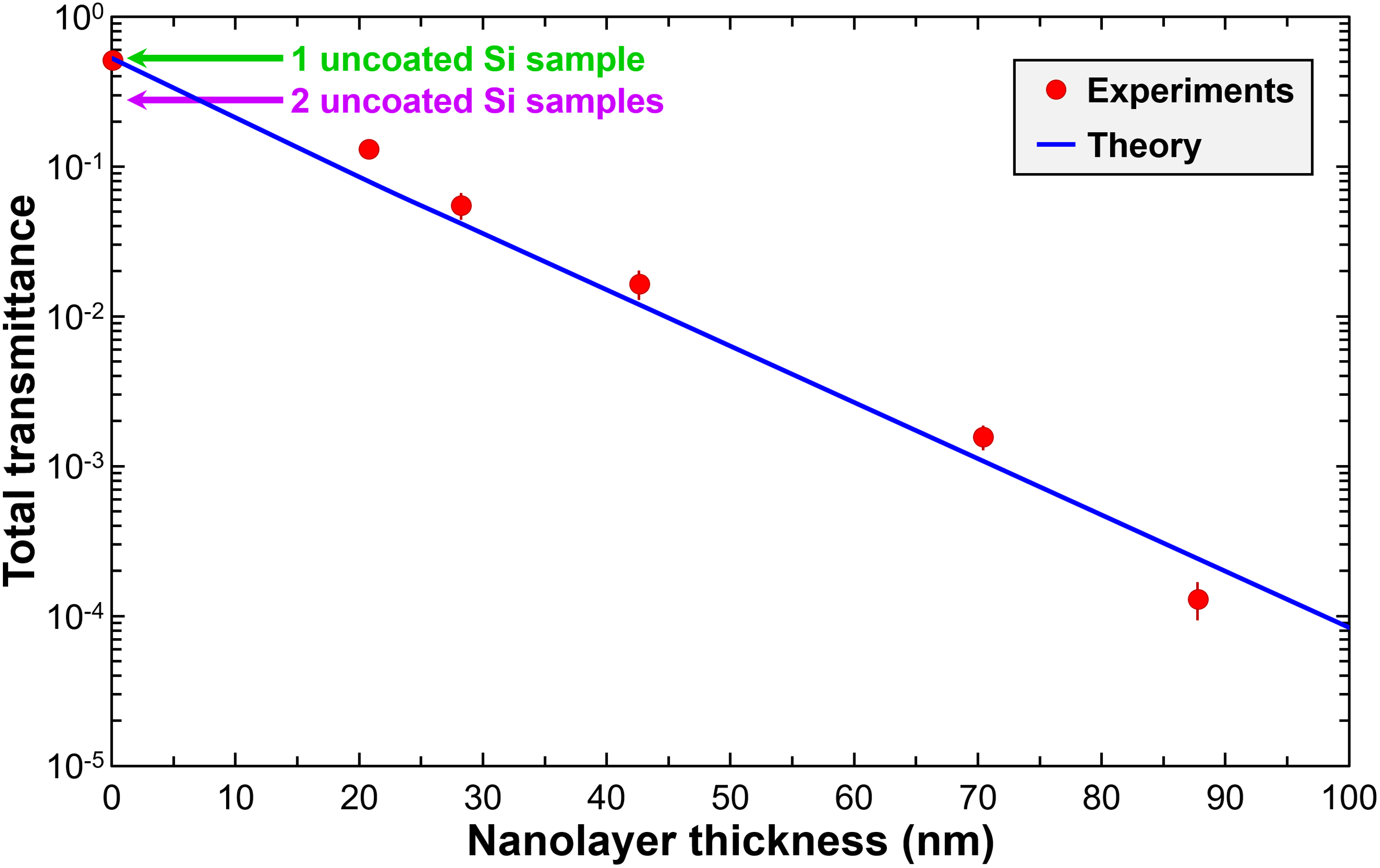
In order to evaluate if the ultrafast laser processing severely alters the optical properties of the samples, the total transmittance has been calculated assuming no decrease caused by the laser-modified zones. To do so, multiple reflections at both air–silicon interfaces, and linear absorption in the gold nanolayer are taken into account with Fresnel equations and Beer–Lambert law, respectively. Under these conditions, as detailed in Section S3.2, Supporting Information, the total transmittance of the welds reads
| (1) |
where and are the Fresnel coefficients for reflection and transmission, respectively, m-1 [47, 48] and are the attenuation coefficient and the thickness of the gold nanolayer, respectively. The corresponding calculations are displayed in Fig. 3 (blue curve). As expected, decreases exponentially with the nanolayer thickness.
These calculations are compared to experimental measurements taken in the irradiated zones (red points). Similar values are obtained when measuring the total transmittance in the non-irradiated zones. Without gold nanolayer, the transmittance of the stack is close to the theoretical value for a single sample (green arrow), which reads , where is the refractive index of silicon at the considered wavelength [see Section S3.1, Supporting Information Eq. (S5)]. In comparison, the theoretical value for the transmittance of two silicon samples with an air gap (, purple arrow) is much lower than the measurements in Fig. 3, which indicates that the samples are in optical contact. For stacks including gold nanolayers, the experimental measurements follow the same trend as the calculations according to Eq. (1). The excellent agreement in Fig. 3 between the measurements and the calculations shows that any additional absorption in the laser-modified zones can be safely neglected. This is consistent with the reduced heat-affected zone produced by ultrashort pulses.
Let us now determine the gold nanolayer thickness for which ultrashort laser welding is the most efficient. The corresponding results are displayed in Fig. 4 (blue points). Without gold nanolayer, the shear joining strength is measured to be kPa. This modest value corresponds to that obtained for samples in optical contact, without laser irradiation. One can thus conclude that the laser irradiation has no effect, in good agreement with the unmodified interface in Fig. 2(b) compared to Figs. 2(c)–(g). In contrast, the bonding is much more effective with a gold nanolayer. This result is independent of the thickness of the silicon sample, provided that the nonlinear focal shift is properly precompensated (see Section S4, Supporting Information). Shear joining strengths MPa are obtained for 21-nm nanolayers, which is comparable to the strengths obtained with adhesive bonding. The striking feature in Fig. 4 is that the thinner the nanolayer, the higher the shear joining strength. This result is not intuitive as a thicker nanolayer leads to higher absorption.
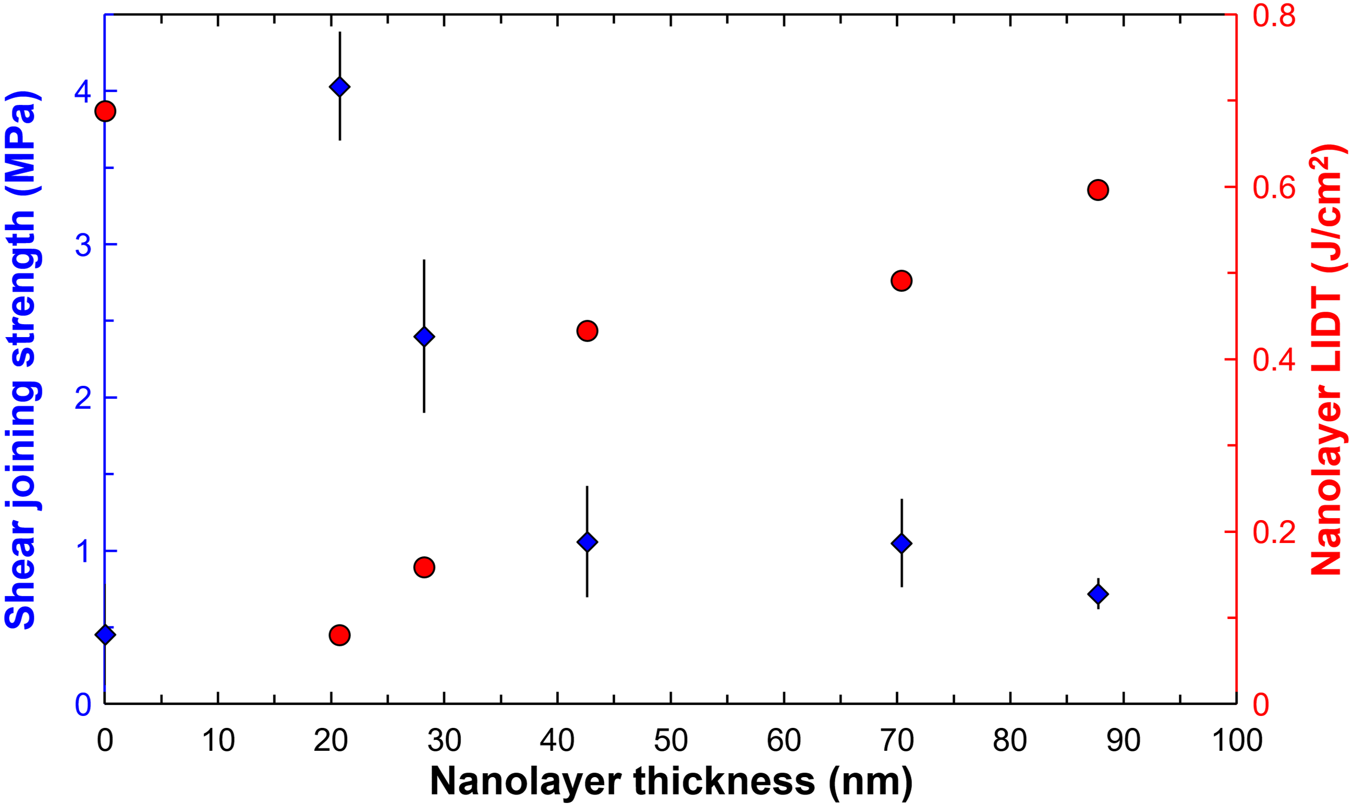
In order to explain this result, the laser-induced damage threshold (LIDT) has been measured for all tested nanolayers (red points in Fig. 4). The LIDT increases with the nanolayer thickness up to a level below that of uncoated silicon, in good agreement with Refs. [49, 50, 51]. In a very recent study, Tsibidis et al. have shown that this behavior is attributable to the inhibition of electron diffusion in thin metallic films, causing the laser-produced hot electrons to remain confined in a restricted volume [52]. Therefore, upon relaxation, the thinner the nanolayer, the higher the energy transferred to the lattice by these “trapped” hot electrons. Consequently, damage is more likely to form for small nanolayers thicknesses, as confirmed by our experimental results in Fig. 4. Given that the pulse energy is kept constant in all our welding experiments, the irradiation of nanolayers with lower LIDT values implies that higher energy densities are obtained. This leads to the conclusion that higher temperatures are reached for nanolayers exhibiting low LIDT, which is favorable for bonding the samples. This is confirmed in Fig. 4 by the opposite trends for the evolution of the shear joining strength and the LIDT of the nanolayer as a function of its thickness.
Ultimately, optical microscopy observations of the welds have been performed after separation. The corresponding images of the initially uncoated top samples are displayed in Fig. 5. Unsurprisingly, no noticeable laser-related features are observed on the exit surface of the top sample when the bottom sample is initially uncoated, which is consistent with Figs. 2 and 4. However, for the thinnest nanolayers ( nm), a pattern caused by the laser irradiation is unambiguously visible. This pattern is also observed for the thickest nanolayers ( nm), except that gold clusters (in yellow) are formed.
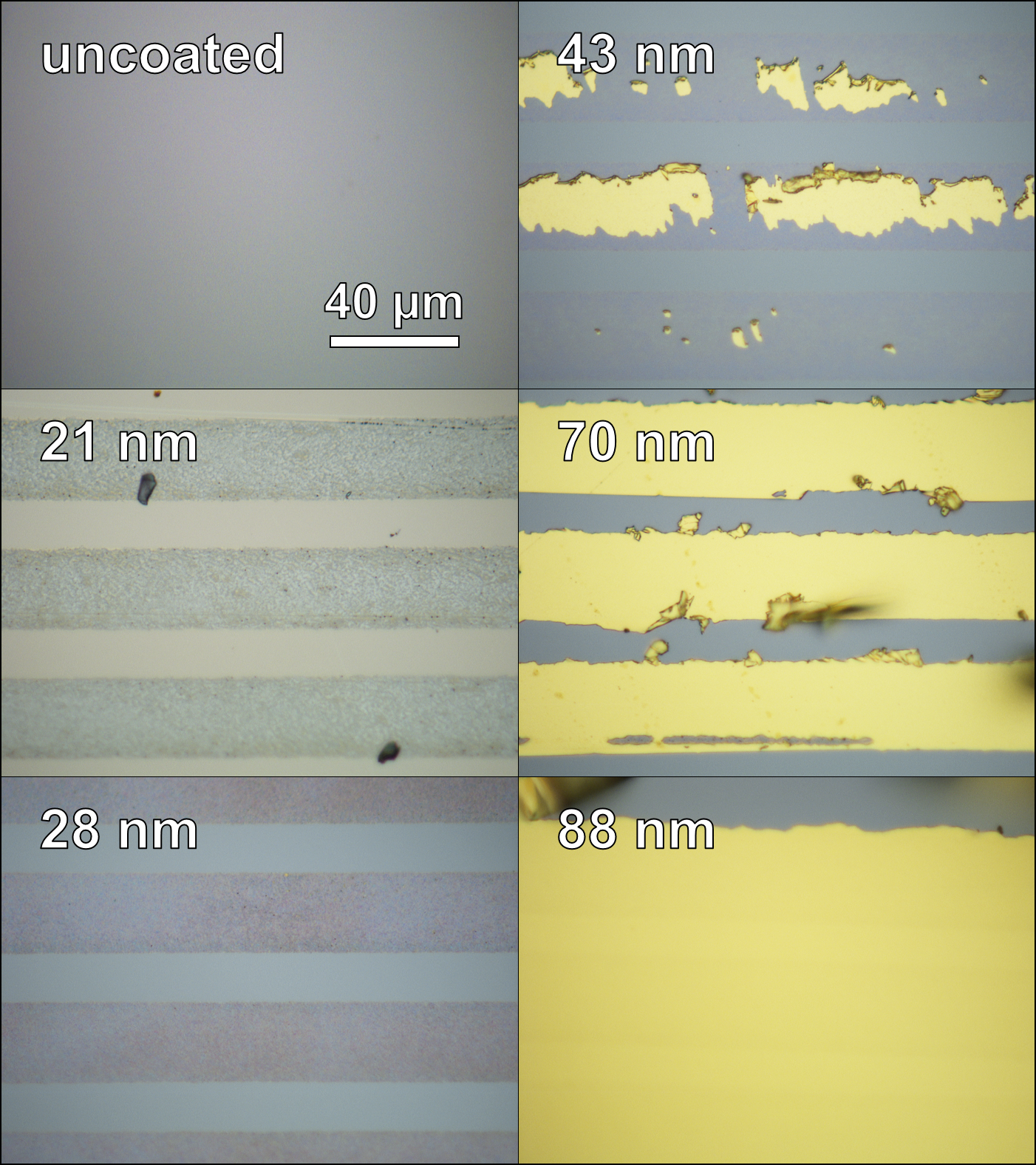
One may note in Fig. 5 that the thicker the nanolayer, the larger the gold areas attached to the top sample. Two conclusions can be drawn from this result. First, for nanolayers nm, the main effect of the laser irradiation is to join the top silicon sample to gold. This is somehow analogous to our recent demonstration of semiconductor–metal ultrafast laser welding [13]. Second, as the bonding strength decreases with increasing nanolayer thickness (see Fig. 4), the strength values for nanolayers nm are attributable to the adhesion of the nanolayer on the bottom sample, and not to any silicon–silicon bonds created at the interface. In contrast, for nanolayers nm, the molten silicon in the top and bottom samples can interpenetrate, and create strong bonds after recrystallization, as supported by Raman spectroscopy in Section S5, Supporting Information. Therefore, the strength values for the thinnest nanolayers in Fig. 4 are not related to their adhesion on the bottom sample.
5. Conclusion
To summarize, we have demonstrated ultrafast laser welding of silicon. This achievement relies on three aspects. First, the silicon samples have been maintained in optical contact during the welding. Second, the precompensation of the nonlinear focal shift leads to optimized energy deposition at the interface between the two silicon samples. Third, the deposition of a gold nanolayer at the interface prior to the welding leads to increased absorption. While introducing another material between two samples may resemble other methods such as adhesive bonding, employing metallic nanolayers ensures that the properties of silicon are not heavily altered. This is all the more confirmed by transmittance measurements which have shown that the laser-induced modifications do not cause additional optical losses. Counterintuitively, the thinnest nanolayers lead to the highest shear joining strengths ( MPa). This is in excellent agreement with the fact that the damage threshold of the nanolayer increases with its thickness, which implies that higher temperatures can be reached at the interface for a constant pulse energy. This result is especially important for envisioning future applications, as the deposition of a few tens of atomic layers of metal (van der Waals radius of gold: 166 pm) should not heavily alter the different properties of silicon. In other words, the technique we propose has to be considered more as local absorption enhancement rather than coating of a few hundred nanometers. To further optimize the silicon–silicon ultrafast laser welding technique, metallic nanolayer thicknesses nm (produced with atomic layer deposition) will be employed. Also, different metallic nanolayers will be tested in the future. In particular, we anticipate that even higher bonding strengths can be reached with optimized metallic nanolayers.
Acknowledgements
The authors thank D. Schelle and C. Otto (Friedrich Schiller University Jena, Institute of Applied Physics, Abbe Center of Photonics, Germany) for nanolayer thickness measurements and wafer cutting, respectively.
Funding
This research has been supported by the Bundesministerium für Bildung und Forschung (BMBF) through the glass2met project, grant No. 13N15290.
Conflict of interest
The authors declare no conflict of interest.
References
- [1] Sören Richter, Felix Zimmermann, Andreas Tünnermann, and Stefan Nolte. Laser welding of glasses at high repetition rates – Fundamentals and prospects. Optics Laser Technology, 83:59–66, sep 2016.
- [2] Richard M. Carter, Jianyong Chen, Jonathan D. Shephard, Robert R. Thomson, and Duncan P. Hand. Picosecond laser welding of similar and dissimilar materials. Applied Optics, 53(19):4233, jul 2014.
- [3] Ilya Mingareev, Fabian Weirauch, Alexander Olowinsky, Lawrence Shah, Pankaj Kadwani, and Martin Richardson. Welding of polymers using a 2-m thulium fiber laser. Optics Laser Technology, 44(7):2095–2099, oct 2012.
- [4] Guodong Zhang and Guanghua Cheng. Direct welding of glass and metal by 1 kHz femtosecond laser pulses. Applied Optics, 54(30):8957, oct 2015.
- [5] Guodong Zhang, Razvan Stoian, Wei Zhao, and Guanghua Cheng. Femtosecond laser Bessel beam welding of transparent to non-transparent materials with large focal-position tolerant zone. Optics Express, 26(2):917, jan 2018.
- [6] E. H. Penilla, L. F. Devia-Cruz, A. T. Wieg, P. Martinez-Torres, N. Cuando-Espitia, P. Sellappan, Y. Kodera, G. Aguilar, and J. E. Garay. Ultrafast laser welding of ceramics. Science, 365(6455):803–808, aug 2019.
- [7] Kristian Cvecek, Sarah Dehmel, Isamu Miyamoto, and Michael Schmidt. A review on glass welding by ultra-short laser pulses. International Journal of Extreme Manufacturing, 1(4):042001, dec 2019.
- [8] Pankaj K. Sahoo, Tao Feng, and Jie Qiao. Dynamic pulse propagation modelling for predictive femtosecond-laser-microbonding of transparent materials. Optics Express, 28(21):31103, oct 2020.
- [9] E V Zavedeev, V V Kononenko, and V I Konov. Delocalization of femtosecond laser radiation in crystalline Si in the mid-IR range. Laser Physics, 26(1):016101, jan 2016.
- [10] V. V. Kononenko, E. V. Zavedeev, and V. M. Gololobov. The effect of light-induced plasma on propagation of intense fs laser radiation in c-Si. Applied Physics A, 122(4):293, apr 2016.
- [11] V. Yu. Fedorov, M. Chanal, D. Grojo, and S. Tzortzakis. Accessing Extreme Spatiotemporal Localization of High-Power Laser Radiation through Transformation Optics and Scalar Wave Equations. Physical Review Letters, 117(4):043902, jul 2016.
- [12] Maxime Chambonneau, David Grojo, Onur Tokel, Fatih Ömer Ilday, Stelios Tzortzakis, and Stefan Nolte. In‐Volume Laser Direct Writing of Silicon—Challenges and Opportunities. Laser Photonics Reviews, 15(11):2100140, nov 2021.
- [13] Maxime Chambonneau, Qingfeng Li, Vladimir Yu Fedorov, Markus Blothe, Kay Schaarschmidt, Martin Lorenz, Stelios Tzortzakis, and Stefan Nolte. Taming Ultrafast Laser Filaments for Optimized Semiconductor–Metal Welding. Laser Photonics Reviews, 15(2):2000433, feb 2021.
- [14] Pol Sopeña, Andong Wang, Alexandros Mouskeftaras, and David Grojo. Transmission Laser Welding of Similar and Dissimilar Semiconductor Materials. Laser Photonics Reviews, 2200208:2200208, aug 2022.
- [15] F. Sari, W. M. Hoffmann, E. Haberstroh, and R. Poprawe. Applications of laser transmission processes for the joining of plastics, silicon and glass micro parts. Microsystem Technologies, 14(12):1879–1886, 2008.
- [16] Ursula Keller, K.J. Weingarten, F.X. Kartner, Daniel Kopf, Bernd Braun, I.D. Jung, Regula Fluck, C. Honninger, Nicolai Matuschek, and J. Aus der Au. Semiconductor saturable absorber mirrors (SESAM’s) for femtosecond to nanosecond pulse generation in solid-state lasers. IEEE Journal of Selected Topics in Quantum Electronics, 2(3):435–453, 1996.
- [17] William W. Zhang, Kim D. Allgood, Michael P. Biskach, Kai-Wing Chan, Michal Hlinka, John D. Kearney, James R. Mazzarella, Ryan S. McClelland, Ai Numata, and Raul E. Riveros. High-resolution, lightweight, and low-cost x-ray optics for the Lynx observatory. Journal of Astronomical Telescopes, Instruments, and Systems, 5(02):1, apr 2019.
- [18] P. C. Verburg, G. R. B. E. Römer, and A. J. Huis in ’t Veld. Two-photon–induced internal modification of silicon by erbium-doped fiber laser. Optics Express, 22(18):21958, sep 2014.
- [19] M. Chambonneau, Q. Li, M. Chanal, N. Sanner, and D. Grojo. Writing waveguides inside monolithic crystalline silicon with nanosecond laser pulses. Optics Letters, 41(21):4875, nov 2016.
- [20] Onur Tokel, Ahmet Turnalı, Ghaith Makey, Parviz Elahi, Tahir Çolakoğlu, Emre Ergeçen, Özgün Yavuz, René Hübner, Mona Zolfaghari Borra, Ihor Pavlov, Alpan Bek, Raşit Turan, Denizhan Koray Kesim, Serhat Tozburun, Serim Ilday, and F. Ömer Ilday. In-chip microstructures and photonic devices fabricated by nonlinear laser lithography deep inside silicon. Nature Photonics, 11(10):639–645, oct 2017.
- [21] M. Chambonneau, D. Richter, S. Nolte, and D. Grojo. Inscribing diffraction gratings in bulk silicon with nanosecond laser pulses. Optics Letters, 43(24):6069, dec 2018.
- [22] Xinya Wang, Xiaoming Yu, Hongyu Shi, Xianhua Tian, Maxime Chambonneau, David Grojo, Brett DePaola, Matthew Berg, and Shuting Lei. Characterization and control of laser induced modification inside silicon. Journal of Laser Applications, 31(2):022601, may 2019.
- [23] Ahmet Turnali, Mertcan Han, and Onur Tokel. Laser-written depressed-cladding waveguides deep inside bulk silicon. Journal of the Optical Society of America B, 36(4):966, apr 2019.
- [24] Xinya Wang, Xiaoming Yu, Matthew J. Berg, Pingping Chen, Brice Lacroix, Sasan Fathpour, and Shuting Lei. Curved waveguides in silicon written by a shaped laser beam. Optics Express, 29(10):14201, may 2021.
- [25] B. N. Chichkov, C. Momma, S. Nolte, F. Alvensleben, and A. Tünnermann. Femtosecond, picosecond and nanosecond laser ablation of solids. Applied Physics A, 63(2):109–115, aug 1996.
- [26] V. V. Parsi Sreenivas, M. Bülters, and R. B. Bergmann. Microsized subsurface modification of mono-crystalline silicon via non-linear absorption. Journal of the European Optical Society: Rapid Publications, 7:12035, sep 2012.
- [27] Margaux Chanal, Vladimir Yu. Fedorov, Maxime Chambonneau, Raphaël Clady, Stelios Tzortzakis, and David Grojo. Crossing the threshold of ultrafast laser writing in bulk silicon. Nature Communications, 8(1):773, dec 2017.
- [28] Markus Blothe, Maxime Chambonneau, and Stefan Nolte. Nanostructured back surface amorphization of silicon with picosecond laser pulses. Applied Physics Letters, 121(10):101602, sep 2022.
- [29] Roland A. Richter, Nikolai Tolstik, Sebastien Rigaud, Paul Dalla Valle, Andreas Erbe, Petra Ebbinghaus, Ignas Astrauskas, Vladimir Kalashnikov, Evgeni Sorokin, and Irina T. Sorokina. Sub-surface modifications in silicon with ultra-short pulsed lasers above 2 m. Journal of the Optical Society of America B, 37(9):2543, sep 2020.
- [30] Evgenii Mareev, Andrey Pushkin, Ekaterina Migal, Kirill Lvov, Sergey Stremoukhov, and Fedor Potemkin. Single-shot femtosecond bulk micromachining of silicon with mid-IR tightly focused beams. Scientific Reports, 12(1):7517, dec 2022.
- [31] Masahiro Mori, Yasuhiko Shimotsuma, Tomoaki Sei, Masaaki Sakakura, Kiyotaka Miura, and Haruhiko Udono. Tailoring thermoelectric properties of nanostructured crystal silicon fabricated by infrared femtosecond laser direct writing. Physica Status Solidi (a), 212(4):715–721, apr 2015.
- [32] Andong Wang, Amlan Das, and David Grojo. Ultrafast Laser Writing Deep inside Silicon with THz-Repetition-Rate Trains of Pulses. Research, 2020:1–11, may 2020.
- [33] M. Chambonneau, M. Blothe, Q. Li, V. Yu. Fedorov, T. Heuermann, M. Gebhardt, C. Gaida, S. Tertelmann, F. Sotier, J. Limpert, S. Tzortzakis, and S. Nolte. Transverse ultrafast laser inscription in bulk silicon. Physical Review Research, 3(4):043037, oct 2021.
- [34] Alan D. Bristow, Nir Rotenberg, and Henry M. van Driel. Two-photon absorption and Kerr coefficients of silicon for 850–2200nm. Applied Physics Letters, 90(19):191104, may 2007.
- [35] Q. Lin, J. Zhang, G. Piredda, R. W. Boyd, P. M. Fauchet, and G. P. Agrawal. Dispersion of silicon nonlinearities in the near infrared region. Applied Physics Letters, 91(2):021111, jul 2007.
- [36] A. Couairon and A. Mysyrowicz. Femtosecond filamentation in transparent media. Physics Reports, 441(2-4):47–189, mar 2007.
- [37] L. Bergé, S. Skupin, R. Nuter, J. Kasparian, and J-P Wolf. Ultrashort filaments of light in weakly ionized, optically transparent media. Reports on Progress in Physics, 70(10):1633–1713, oct 2007.
- [38] S. Richter, F. Zimmermann, R. Eberhardt, A. Tünnermann, and S. Nolte. Toward laser welding of glasses without optical contacting. Applied Physics A, 121(1):1–9, oct 2015.
- [39] Hua Tan and Ji’an Duan. Welding of glasses in optical and partial-optical contact via focal position adjustment of femtosecond-laser pulses at moderately high repetition rate. Applied Physics A, 123(7):481, jul 2017.
- [40] Alessandro Alberucci, Namig Alasgarzade, Maxime Chambonneau, Markus Blothe, Helena Kämmer, Gabor Matthäus, Chandroth P. Jisha, and Stefan Nolte. In-Depth Optical Characterization of Femtosecond-Written Waveguides in Silicon. Physical Review Applied, 14(2):024078, aug 2020.
- [41] Shuting Lei, David Grojo, Jianfeng Ma, Xiaoming Yu, and Han Wu. Femtosecond Laser Backside Ablation of Gold Film on Silicon Substrate. Procedia Manufacturing, 5:594–608, 2016.
- [42] I. Astrauskas, B. Považay, A. Baltuška, and A. Pugžlys. Influence of 2.09-m pulse duration on through-silicon laser ablation of thin metal coatings. Optics Laser Technology, 133(August 2020):106535, jan 2021.
- [43] InFocus, 2021. https://github.com/QF06/InFocus.
- [44] Qingfeng Li, Maxime Chambonneau, Markus Blothe, Herbert Gross, and Stefan Nolte. Flexible, fast, and benchmarked vectorial model for focused laser beams. Applied Optics, 60(13):3954, may 2021.
- [45] Q. Li, F. Luo, G. Matthäus, and S. Nolte. Direct Glass-to-Metal Welding by Femtosecond Laser Pulse Bursts: II, Effects of Materials Pairs and Beam Shapes. unpublished, 2022.
- [46] H. H. Li. Refractive index of silicon and germanium and its wavelength and temperature derivatives. Journal of Physical and Chemical Reference Data, 9(3):561–658, jul 1980.
- [47] Dmitry I. Yakubovsky, Aleksey V. Arsenin, Yury V. Stebunov, Dmitry Yu. Fedyanin, and Valentyn S. Volkov. Optical constants and structural properties of thin gold films. Optics Express, 25(21):25574, 2017.
- [48] Gilad Rosenblatt, Boris Simkhovich, Guy Bartal, and Meir Orenstein. Nonmodal Plasmonics: Controlling the Forced Optical Response of Nanostructures. Physical Review X, 10(1):11071, 2020.
- [49] E. Matthias, M. Reichling, J. Siegel, O. W. Käding, S. Petzoldt, H. Skurk, P. Bizenberger, and E. Neske. The influence of thermal diffusion on laser ablation of metal films. Applied Physics A Solids and Surfaces, 58(2):129–136, 1994.
- [50] B. C. Stuart, M. D. Feit, S. Herman, A. M. Rubenchik, B. W. Shore, and M. D. Perry. Optical ablation by high-power short-pulse lasers. Journal of the Optical Society of America B, 13(2):459, 1996.
- [51] Jörg Krüger, Daniela Dufft, Robert Koter, and Andreas Hertwig. Femtosecond laser-induced damage of gold films. Applied Surface Science, 253(19):7815–7819, 2007.
- [52] G.D. Tsibidis, D. Mansour, and E. Stratakis. Damage threshold evaluation of thin metallic films exposed to femtosecond laser pulses: The role of material thickness. Optics Laser Technology, 156(July):108484, dec 2022.