Quantum Monte Carlo Study of Semiconductor Artificial Graphene Nanostructures
Abstract
Semiconductor artificial graphene nanostructures where Hubbard model parameter can be of the order of 100, provide a highly controllable platform to study strongly correlated quantum many-particle phases. We use accurate variational and diffusion Monte Carlo methods to demonstrate a transition from antiferromagnetic to metallic phases for experimentally accessible lattice constant nm in terms of lattice site radius , for finite sized artificial honeycomb structures nanopatterned on GaAs quantum wells containing up to 114 electrons. By analysing spin-spin correlation functions for hexagonal flakes with armchair edges and triangular flakes with zigzag edges, we show that edge type, geometry and charge nonuniformity affect the steepness and the crossover value of the phase transition. For triangular structures, the metal-insulator transition is accompanied with a smoother edge polarization transition.
In recent years, technological advances in photonic and condensed matter based artificial superlattices gives us opportunities to develop practical quantum simulators [1, 2, 3, 4, 5, 6, 7, 8, 9, 10, 11, 12, 13, 14]. These quantum simulators allow us to replicate complex systems that are hard to fabricate and provide us with a playground to verify theoretical predictions. In this respect, artificial graphene (AG) nanostructures, designed by imitating the 2D honeycomb pattern of graphene, have been proven to be good candidates for being reliable and controllable sources for both fabrication and investigation of many physical phenomena related to Dirac fermions [15, 16, 17, 18, 13, 14, 19]. In particular, AG nanostructures can be formed using semiconductor materials. While earlier reports on nanopatterned artificial graphene on GaAs quantum well (QW) structures found no evidence of massless Dirac fermions (MDFs), presumably because of the relatively large lattice periods [20, 21, 22], in recent experimental works using modulation-doped AlGaAs/GaAs quantum wells [14, 13] shrinking down of the lattice constant of the honeycomb array to approximately 50 nm allowed the observation of the predicted graphene-like behavior [21, 23, 24, 25].
Observation of Dirac fermions in AG also opens up a fresh way of studying graphene quantum dots [26] where geometry, size and edge type is expected to give rise to several physical properties such as bandgap opening [27], edge magnetization [28, 29, 30] and optical control [31]. However, the fabrication and reliability issues such as edge reconstruction or presence of impurities, make it harder to observe interesting phenomena predicted to occur in nanostructured graphene. Semiconductor AG nanostructures, on the other hand, offer several advantages such as tunability of system parameters including lattice constant, site radius and potential depth, which, in turn, allow to control electron-electron interactions and tunneling strength between sites, in particular Hubbard parameter . In experimental structures with lattice constant nm [14], can be as high as 350 (as we will argue below) i.e. two orders of magnitude larger than the critical value for antiferromagnetic Mott transition predicted by calculations based on Hubbard model for honeycomb lattice [32, 33, 34, 35]. Moreover, unlike in real graphene, long range electron repulsion does not cancel the attraction of the artificial confining potential in AG even near charge neutrality. For such large and long-ranged electron interactions, a non-perturbative many-body approach is desirable for careful treatment of correlation effects.
Earlier theoretical work on electron interaction effects in semiconductor AG nanostructures based on density functional theory (DFT) showed that Dirac bands were stable against interactions [23, 24] which was also confirmed using path integral Monte Carlo calculations [25]. However, recent calculations using Hartree-Fock and exact diagonalization approaches for a triangular zigzag geometry with nm show that a transition from antiferromagnetic (AF) insulator to metallic phases occurs, pointing to the importance of electron interactions [36].
In this work, we use continuum variational Monte Carlo (VMC) and diffusion Monte Carlo (DMC) methods for non-perturbative and accurate treatment of many-body correlations within the fixed-node approximation to study GaAs based AG nanostructures. First, we consider an hexagonal armchair geometry which serves as a bridge between the finite-size samples and bulk graphene [27], with lattice constant nm following recent experimental work [14]. We show that, a transition from AF to metallic phase occurs, but is affected by a nonuniform charge distribution in the sample due to finite size effects. This charge nonuniformity which is not present in real graphene quantum dots, causes the phase transition to be steeper and to occur at a smaller value of . We also investigate AG quantum dots with triangular zigzag geometry and show that edge magnetization survives the phase transition, in agreement with previous theoretical prediction for smaller lattice constants [36].
Our model of nanostructured semiconductor AG consists of interacting electrons in a honeycomb array of confining potentials, described by the many-body Hamiltonian
| (1) |
in effective atomic units (electronic charge , dielectric constant , effective mass , and are set to 1), where is the Coulomb interaction between the electrons, is the total potential energy of the confining potentials, and is the spring constant of quadratic gate potential located at the center of the system which controls the finite size effects. Typical material properties for GaAs, effective electron mass and dielectric constant , are used. Corresponding effective Bohr radius is nm, and the effective Hartree energy is meV. The honeycomb array of potential wells is modelled using gaussian-like functions [25],
| (2) |
where , is the potential depth, is the radius and is the sharpness of the potential wells. is the location of the potential wells. In our numerical calculations, dot-to-dot distance (lattice constant) was fixed to nm, while several radius values from nm to nm were covered. Three different sharpness values were used; for a gaussian potential, for a sharp, muffin-tin like potential, and in between. values vary depending on dot radius (e.g. increasing monotonically with dot radius from meV to meV for and ), tuned to keep the total energy of the system close to zero, since our aim is to imitate the charge neutral behavior of finite sized graphene quantum dot. For too high values of , electrons tend to escape the system during VMC or DMC simulations, while for too low values over localization occurs [21].
Accuracy of the numerical calculations depends on trial wave functions in both VMC and DMC methods. One starts with a set of single-particle orbitals (e.g. localized gaussians or from self-consistent calculations) to build a Slater-Jastrow trial wave function which is a linear combination of products of up- and down-spin Slater determinants of these orbitals multiplied by a Jastrow factor (The details of our Jastrow factor is given in Ref. 37). After the VMC calculations where Jastrow parameters as well as the gaussian functions width are optimized using energy minimization technique [38], we use fixed-node DMC [39, 40] to project the optimized many-body wave function onto a better approximation of the true ground state, an approximation that has the same nodes as . The resulting fixed-node DMC energy is an upper bound to the true energy and depends only on the nodal structure of the Slater part of the trial wave function [39].
In order to form Slater determinants, we prepare three different types of orbitals aiming to capture metallic or AF insulator phases, depending on the potential well radius : (i) Localized gaussian functions that are proven to be one of the most suitable functions for 2D systems of quantum dots [37, 41, 42] and are expected to provide a better description of strongly localized states. (ii) Tight-binding (TB) orbitals, on the other extreme, may be used to describe metallic phases in which electrons move more freely. (iii) Mean-field Hubbard (MFH) orbitals can describe both localized and liquid-like states depending on the ratio . Corresponding variational and fixed-node energies of those three types of orbitals are expected to hint us at a possible transition from metallic state to an AF order as a function of . In this work, all quantities that do not commute with the Hamiltonian were calculated using an extrapolated estimator, [39].
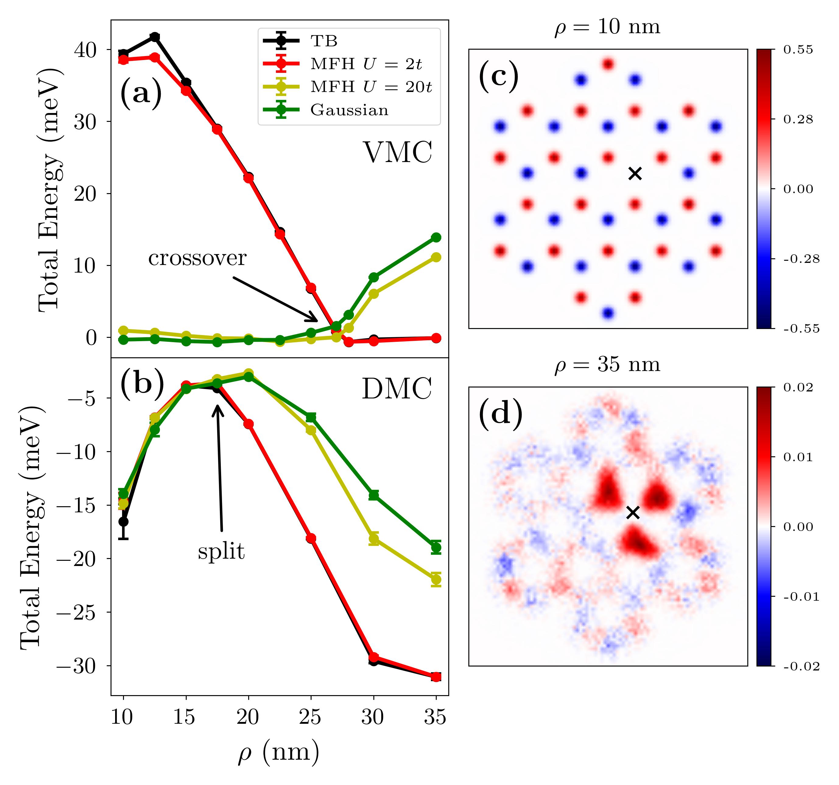
Figure 1a shows the VMC energies obtained from TB, MFH and gaussian orbitals, as a function of , for an armchair hexagonal geometry with 42 sites and 42 electrons. The parabolic gate potential parameter is turned off () and its effect will be discussed in a later section. At low , gaussian and MFH orbitals provides better variational energies. As is increased to nm, a clear crossover (from insulator to metallic phase) occurs above which TB and MFH orbitals take the lead. Fixed-node DMC energies, however, reveal a somewhat different picture, shown in Fig. 1b. From nm to nm, all trial wave functions give similar energies within the statistical error bars, and split near nm. After the split, the ground state of the system is represented by TB and MFH trial wave functions. These results show that, surprisingly, TB trial wave function has equally good nodal structure as the gaussian orbitals at low values, raising questions about the true nature of the ground state. To reveal the underlying electronic and magnetic structure, we consider the pair densities , probability of finding an electron with spin at location r when an electron with spin is fixed at location , and the pair spin densities, . Figures 1c-d show the pair spin densities for a reference spin down electron fixed on top of a site (chosen to break the system symmetry and away from the edges) shown with a cross. At nm, electrons are well localized at the sites, leading to an AF insulator. On the other hand, at large values of , spin-spin correlations are weak and short-ranged up to nearest neighbors. While these results confirm that a transition from AF insulator to a metallic phase does occur as observed in previous work [36], there are several issues left to address: (i) Inconsistent signature regarding the crossover value obtained from VMC and DMC energies and the underlying dynamics of the transition. (ii) Finite size and edge effects. (iii) Relationship to bulk properties.
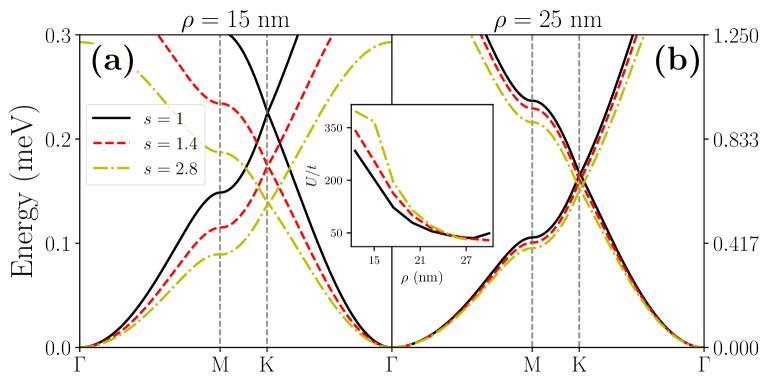
Now, we turn our attention to the 2D bulk properties for similar system parameters used in our calculations. As mentioned earlier, values are tuned to keep the total energy of the system close to zero. The question is whether such set of parameters leave the Dirac cone structure intact, which may otherwise have repercussions on electronic and magnetic properties. In Fig. 2, we show our DFT calculations results in the local density approximation (LDA). The Dirac cone structure is preserved for the range nm; outside this range the Dirac fermion picture becomes distorted. Moreover, we can estimate the TB hopping parameter from the slope of the Dirac cones as where is the lattice constant. As we see from Fig. 2, increases with increasing but decreasing , as expected. In addition to , to build a Hubbard model, we estimated the value for a single well using after solving single particle Schrödinger equation. In the inset of Fig. 2, we plot as a function of which shows a fast decay from to 50 between and . Surprisingly, these results indicate that the critical value for metal-insulator transition in AG is much higher than the critical value of predicted by Hubbard calculations [32, 33, 34, 35], presumably due to the importance of long-range interactions and deviation from the nearest neighbor TB approximation as increases. On the other hand, according to our quantum Monte Carlo (QMC) calculations, MFH trial wave functions based on LDA estimation of do not provide the most suitable fixed-node energies and the nodal structure of the simplest TB trial wave functions works best for the whole range of system parameters regardless of the underlying electronic or magnetic state.
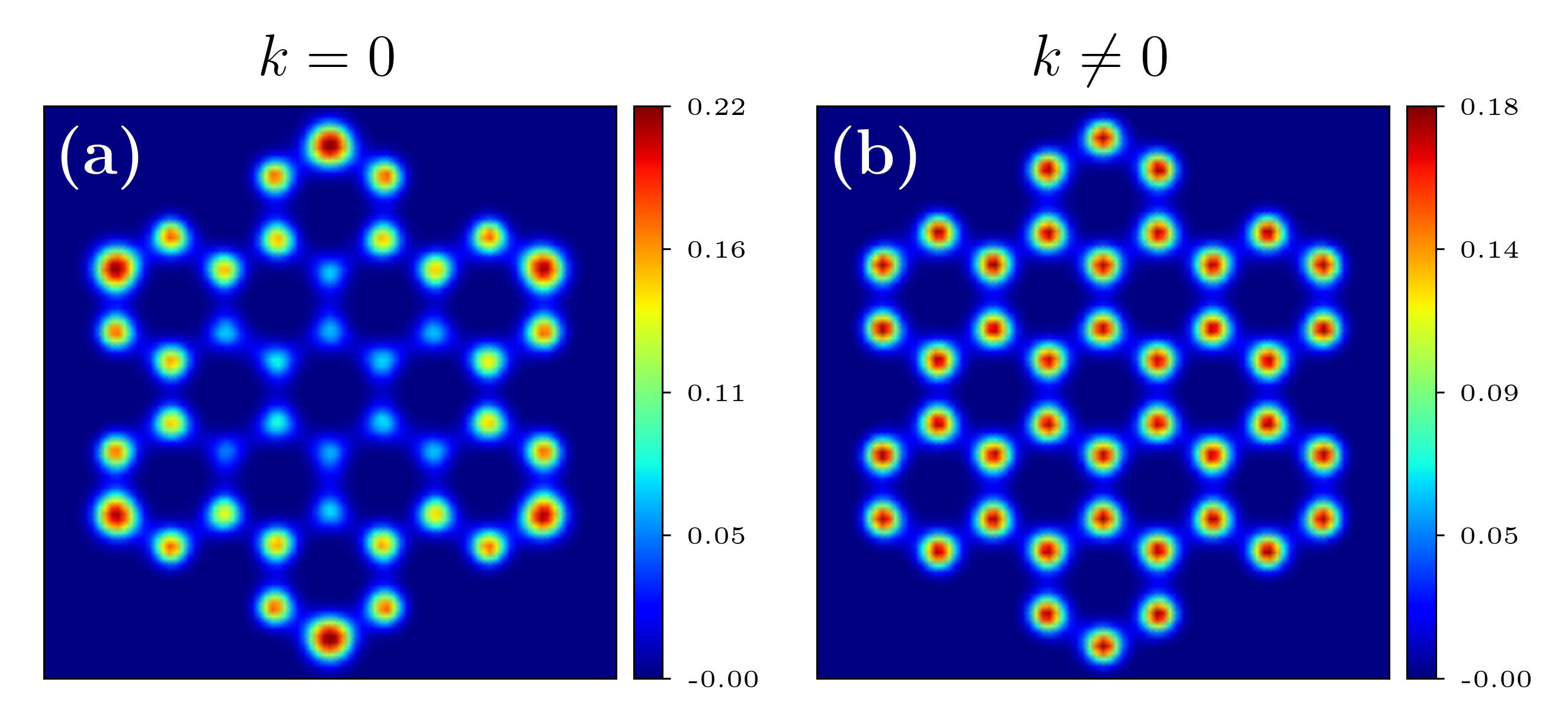
Next, we focus on finite size effects. While is tuned to imitate overall charge neutrality, long-range electron interactions still affects the charge distribution inside the system, pushing the electrons towards the edges and/or corners, as can be seen in Fig. 3a for the hexagonal armchair system with , and nm. While, in principle, can be decreased further to achieve charge uniformity, this would localize the electrons too strongly to their sites and make the system negatively charged unlike in real graphene systems. An alternative solution is to apply a quadratic gate potential controlled by the parameter in Eq. (1). When , quadratic gate potential attracts the electrons towards the center of the system so that the charge uniformity is preserved, and finite size effects are minimized, as shown in Fig. 3b for meV/nm2.
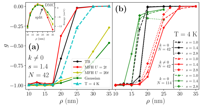
In order to understand more in detail the dynamics of the transition from AF insulator to metallic phase including effects of charge nonuniformity and quantum well potential sharpness, we consider a real space spin-spin correlation function normalized by the density-density correlations, where and are the average total spin and total electron densities on site i within a radius , and are the nearest neighbor sites. We used in all spin-spin correlation calculations, where is the lattice constant. Output values of the function remain in [-1,1] range, with corresponding to AF and corresponding to metallic configuration ( means that all spins are in the same direction, which does not happen in the subspace considered here). In Fig. 4a, is plotted against obtained from different trial wave functions, for and meV/nm2 to obtain charge uniformity. We have also added a weighted average of all trial wave functions using Boltzmann distribution at K, representing the ground state, to ensure that no effects are missed when various trial wave functions lead to same ground state energies within statistical noise. The emerging picture is that the system remains strongly AF between nm, then starts fading smoothly, finally reaching fully metallic regime around nm. We note that the DMC energies for split around nm (see the inset of Fig. 4a), in contrast with the results in Fig. 1b where the split occurs near nm. Figure 4b summarizes all weight averaged values obtained for different and values, and for both flake sizes. Interestingly, for the transition from AF to metallic regime is sharper than for charge uniform systems (), albeit at lower values. Sharpness and system size , on the other hand, does not have a significant effect on the transitions.
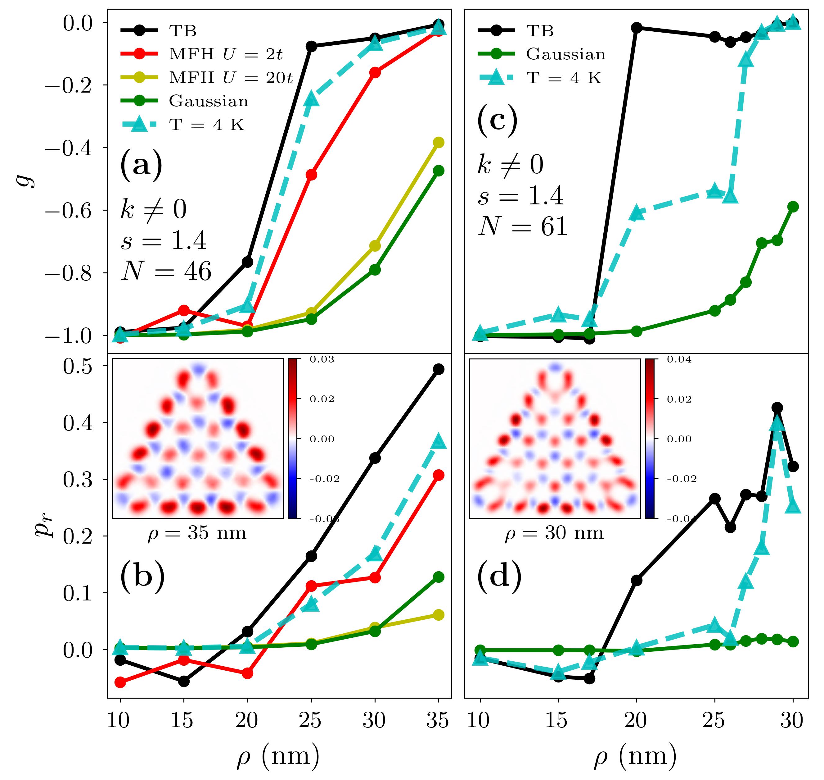
For triangular zigzag structures, spin polarized edges even in the metallic phase is expected due to the imbalance between the two sublattices [28, 29, 30, 43, 36], with a non-zero ground state total spin where and are number of and sublattice atoms, according to Lieb’s theorem [44]. In our AG flake, the total spin is for and for . The analysis of the spin-spin correlation functions for and meV/nm2 leads to a similar picture as before; the system with sites is perfectly AF between nm, then smoothly vanishes between nm, before becoming completely metallic. For sites, although the transition is not as smooth presumably due to larger statistical fluctuations at large system size, a similar picture emerges (Fig. 5c). In order to understand the edge magnetization during the transition, we consider an edge polarization ratio defined as
| (3) |
which gives one if only edge sites are polarized, zero if edge and bulk sites are equally (un)polarized. In Fig. 5b, edge polarization ratio increases as increases, indicating that spins are polarized more at the edges as the system goes into metallic phase similar to real triangular zigzag graphene quantum dots, and consistent with the spin density results in Fig. 5b and 5d insets, demonstrating a metallic phase with edge-polarized spins at nm for 46 sites and at nm for 61 sites. Additionally, in Fig. 5, weighted average analysis also confirms that the triangular zigzag AG flake undergoes a metal-insulator transition between and nm dot radius. However, the edge polarization transition occurs slower compared to the metal insulator transition.
In summary, we have shown that a metal - antiferromagnetic insulator transition occurs in nanopatterned GaAs based artificial graphene structures including up to electrons with lattice constant nm as a function of site radius, using accurate variational and diffusion Monte Carlo methods, within the Dirac regime as confirmed by our density functional calculations. Our approach where a simple tight-binding trial wave function combined with a Jastrow factor is found to be sufficient to account for electron correlation effects in both metallic and antiferromagnetic regimes, allows direct modelling of system parameters, making it possible to systematically investigate the effects of edge type, geometry, size, quantum well shape and gate potentials. We have shown that the steepness and the crossover value of the phase transition is affected by charge nonuniformity due to finite size effects. For triangular structures exhibiting magnetized edge states, the edge polarization transition is shown to occur more slowly compared to the metal insulator transition.
Acknowledgements.
We thank C. J. Umrigar for his endless support for CHAMP [45] program with which our QMC simulations have been performed, Pawel Hawrylak and Yasser Saleem for valuable conversations. This work was supported by The Scientific and Technological Research Council of Turkey (TUBITAK) under the 1001 Grant Project Number 119F119. The numerical calculations reported in this study were partially performed at TUBITAK ULAKBIM, High Performance and Grid Computing Center (TRUBA resources).References
- Bloch [2005] I. Bloch, Nat. Phys. 1, 23 (2005).
- Mazurenko et al. [2017] A. Mazurenko, C. S. Chiu, G. Ji, M. F. Parsons, M. Kanász-Nagy, R. Schmidt, F. Grusdt, E. Demler, D. Greif, and M. Greiner, Nature 545, 462 (2017).
- Buluta and Nori [2009] I. Buluta and F. Nori, Science 326, 108 (2009).
- Kuhr [2016] S. Kuhr, Natl. Sci. Rev. 3, 170 (2016).
- Weimer et al. [2010] H. Weimer, M. Müller, I. Lesanovsky, P. Zoller, and H. P. Büchler, Nat. Phys. 6, 382 (2010).
- Islam et al. [2011] R. Islam et al., Nat. Commun. 2, 377 (2011).
- Salfi et al. [2016] J. Salfi, J. A. Mol, R. Rahman, G. Klimeck, M. Y. Simmons, L. C. L. Hollenberg, and S. Rogge, Nat. Commun. 7, 11342 (2016).
- Hempel et al. [2018] C. Hempel et al., Phys. Rev. X 8, 031022 (2018).
- Aspuru-Guzik and Walther [2012] A. Aspuru-Guzik and P. Walther, Nat. Phys. 8, 285 (2012).
- Cai et al. [2013] J. Cai, A. Retzker, F. Jelezko, and M. B. Plenio, Nat. Phys. 9, 168 (2013).
- Bernien et al. [2017] H. Bernien et al., Nature 551, 579 (2017).
- Li et al. [2021] T. Li et al., Nature 597, 350 (2021).
- Du et al. [2018] L. Du et al., Nat. Commun. 9, 3299 (2018).
- Wang et al. [2018] S. Wang et al., Nat. Nanotechnol. 13, 29 (2018).
- Gomes et al. [2012] K. K. Gomes, W. Mar, W. Ko, F. Guinea, and H. C. Manoharan, Nature 483, 306 (2012).
- Tarruell et al. [2012] L. Tarruell, D. Greif, T. Uehlinger, G. Jotzu, and T. Esslinger, Nature 483, 302 (2012).
- Lu et al. [2014] L. Lu, J. D. Joannopoulos, and M. Soljačić, Nat. Photonics 8, 821 (2014).
- Jacqmin et al. [2014] T. Jacqmin, I. Carusotto, I. Sagnes, M. Abbarchi, D. D. Solnyshkov, G. Malpuech, E. Galopin, A. Lemaître, J. Bloch, and A. Amo, Phys. Rev. Lett. 112, 116402 (2014).
- Wang et al. [2016] S. Wang, D. Scarabelli, Y. Y. Kuznetsova, S. J. Wind, A. Pinczuk, V. Pellegrini, M. J. Manfra, G. C. Gardner, L. N. Pfeiffer, and K. W. West, Appl. Phys. Lett. 109, 113101 (2016).
- Nádvorník et al. [2012] L. Nádvorník et al., New J. Phys. 14, 053002 (2012).
- Gibertini et al. [2009] M. Gibertini, A. Singha, V. Pellegrini, M. Polini, G. Vignale, A. Pinczuk, L. N. Pfeiffer, and K. W. West, Phys. Rev. B 79, 241406 (2009).
- Singha et al. [2011] A. Singha et al., Science 332, 1176 (2011).
- Räsänen et al. [2012] E. Räsänen, C. A. Rozzi, S. Pittalis, and G. Vignale, Phys. Rev. Lett. 108, 246803 (2012).
- Kylänpää et al. [2015] I. Kylänpää, M. Aichinger, S. Janecek, and E. Räsänen, J. Phys. Condens. Matter 27, 425501 (2015).
- Kylänpää et al. [2016] I. Kylänpää, F. Berardi, E. Räsänen, P. García-González, C. A. Rozzi, and A. Rubio, New J. Phys. 18, 083014 (2016).
- Güçlü et al. [2014] A. D. Güçlü, P. Potasz, M. Korkusinski, and P. Hawrylak, Graphene Quantum Dots (Springer, Berlin, Heidelberg, 2014).
- Güçlü et al. [2010] A. D. Güçlü, P. Potasz, and P. Hawrylak, Phys. Rev. B 82, 155445 (2010).
- Fernández-Rossier and Palacios [2007] J. Fernández-Rossier and J. J. Palacios, Phys. Rev. Lett. 99, 177204 (2007).
- Wang et al. [2008] W. L. Wang, S. Meng, and E. Kaxiras, Nano Lett. 8, 241 (2008).
- Güçlü et al. [2009a] A. D. Güçlü, P. Potasz, O. Voznyy, M. Korkusinski, and P. Hawrylak, Phys. Rev. Lett. 103, 246805 (2009a).
- Güçlü and Hawrylak [2013] A. D. Güçlü and P. Hawrylak, Phys. Rev. B 87, 035425 (2013).
- Assaad and Herbut [2013] F. F. Assaad and I. F. Herbut, Phys. Rev. X 3, 031010 (2013).
- Otsuka et al. [2016] Y. Otsuka, S. Yunoki, and S. Sorella, Phys. Rev. X 6, 011029 (2016).
- Buividovich et al. [2019] P. Buividovich, D. Smith, M. Ulybyshev, and L. von Smekal, Phys. Rev. B 99, 205434 (2019).
- Ostmeyer et al. [2020] J. Ostmeyer, E. Berkowitz, S. Krieg, T. A. Lähde, T. Luu, and C. Urbach, Phys. Rev. B 102, 245105 (2020).
- Saleem et al. [2022] Y. Saleem, A. Dusko, M. Cygorek, M. Korkusinski, and P. Hawrylak, Phys. Rev. B 105, 205105 (2022).
- Güçlü et al. [2005] A. D. Güçlü, G. S. Jeon, C. J. Umrigar, and J. K. Jain, Phys. Rev. B 72, 205327 (2005).
- Umrigar et al. [2007] C. J. Umrigar, J. Toulouse, C. Filippi, S. Sorella, and R. G. Hennig, Phys. Rev. Lett. 98, 110201 (2007).
- Foulkes et al. [2001] W. M. C. Foulkes, L. Mitas, R. J. Needs, and G. Rajagopal, Rev. Mod. Phys. 73, 33 (2001).
- Umrigar et al. [1993] C. J. Umrigar, M. P. Nightingale, and K. J. Runge, J. Chem. Phys. 99, 2865 (1993).
- Ghosal et al. [2006] A. Ghosal, A. D. Güçlü, C. J. Umrigar, D. Ullmo, and H. U. Baranger, Nat. Phys. 2, 336 (2006).
- Güçlü et al. [2009b] A. D. Güçlü, C. J. Umrigar, H. Jiang, and H. U. Baranger, Phys. Rev. B 80, 201302 (2009b).
- Su et al. [2019] J. Su et al., Sci. Adv. 5, eaav7717 (2019).
- Lieb [1989] E. H. Lieb, Phys. Rev. Lett. 62, 1201 (1989).
- [45] CHAMP, a quantum Monte Carlo program written by C. J. Umrigar, C. Filippi and Julien Toulouse, extended to 2D systems by A. D. Güçlü.