Spin Hall angle in single-layer graphene
Abstract
We investigate the spin Hall effect in a single-layer graphene device with disorder and interface-induced spin-orbit coupling. Our graphene device is connected to four semi-infinite leads that are embedded in a Landauer-Büttiker setup for quantum transport. We show that the spin Hall angle of graphene devices exhibits mesoscopic fluctuations that are similar to metal devices. Furthermore, the product between the maximum spin Hall angle deviation and dimensionless longitudinal conductivity follows a universal relationship . Finally, we compare the universal relation with recent experimental data and numerically exact real-space simulations from the tight-binding model.
I Introduction
The idea to manipulate information through spin was first introduced by Datta and Das Datta and Das (1990) and it has enhanced the development of spintronics in the last two decades Sayed et al. (2021); Jedema et al. (2003); Lou et al. (2007); Hirohata and Takanashi (2014); Wang, Alzate, and Amiri (2013). This idea aims to use spin as an information carrier in place of charge, which makes high-speed computing possible. Spintronics can be activated by spin-orbit coupling (SOC), which is the key to controlling spin transport properties without magnetic materials. SOC is a relativistic effect that is found in many branches of condensed matter physics. The spin Hall effect (SHE) is one of the most significant phenomena observed in spintronics Hirsch (1999); Dyakonov and Perel (1971a, b); Schliemann (2006); Sinova et al. (2015); Seifert et al. (2018); Wang et al. (2015), which allows us to obtain a spin current from a charge current. More specifically, when a longitudinal charge current crosses a region with a strong SOC, it converts to a transversal spin current. Therefore, the spin Hall angle (SHA) is an important parameter that is commonly used to quantify a material’s ability to convert charge-to-spin currents. The SHA is defined as the ratio between the spin Hall current and the charge current, and its experimental values can vary from to for different materials in a disordered regime Ando and Saitoh (2012); Althammer et al. (2013); Sagasta et al. (2016); Fritz et al. (2018); Pai et al. (2012); Lou et al. (2020); Okano et al. (2019); Zhu, Ralph, and Buhrman (2018); Wang et al. (2014); Alves-Santos et al. (2017); Alves Santos et al. (2019); Zhang et al. (2015).
The presence of disorder leads to universal spin Hall current fluctuations Nikolić, Zârbo, and Souma (2005); Nikolić, B. K. and Zârbo, L. P. (2007); Ren et al. (2006); Bardarson, Adagideli, and Jacquod (2007); Qiao et al. (2008); Ramos et al. (2012); Vasconcelos, Ramos, and Barbosa (2016), similar to universal charge current fluctuations Beenakker (1997). Therefore, it is necessary to investigate the SHA fluctuations to obtain information about the universality of converting a charge current into a spin current. Ref. Santana et al., 2020 started this investigation in an analytical, numerical and experimental analysis of metals. The authors show that for a quasi-unidimensional sample, the maximum SHA deviation follows a relationship with dimensionless longitudinal conductivity , where , and are number of propagating wave modes, device longitudinal length and free electron path, respectively, which is given by . This proves that vanishing SHE—that is, when spin Hall conductivity is zero for any nonvanishing disorder strength Inoue, Bauer, and Molenkamp (2004); Raimondi and Schwab (2005); Dimitrova (2005); Khaetskii (2006); Nikolić, Zârbo, and Souma (2005); Nikolić, B. K. and Zârbo, L. P. (2007); Milletarì et al. (2017)—is irrelevant for a realistic finite-size device where self-averaging over an infinite system size is avoided.
The use of two-dimensional materials, such as graphene, in electronic systems has been of great interest because of their ability to transport spin over long distances at room temperature, which optimises transport Novoselov et al. (2004); Geim and Novoselov (2007); Castro Neto et al. (2009); Avsar et al. (2020); Ingla-Aynés et al. (2015). However, it is well-known that graphene has a low SOC Castro Neto et al. (2009). Therefore, several techniques have been proposed to improve its spin current generation capacity to circumvent this problem Avsar et al. (2020); Ingla-Aynés et al. (2015); Garcia et al. (2018); Schubert, Schleede, and Fehske (2009); Wang and Wu (2015); Islam and Benjamin (2016); Balakrishnan et al. (2013).
Ref. Balakrishnan et al., 2013 reported the first experimental realisation of the SHE in graphene. To increase the SOC, the authors added covalently bonded hydrogen atoms to graphene in a controlled manner. As a result, they obtained a SHE that is an order of magnitude greater than that observed in metals. This method also allowed measurements to be performed at room temperature, getting a value for the SHA at the charge-neutrality (Dirac) point (CNP) of . They then extended their studies to single-layer graphene doped with metallic atoms Balakrishnan et al. (2014). The value obtained for SHA at room temperature was . This result shows that the interaction with metals produces equally strong effects, as observed in the former experiment. These experiments represent a significant advance in applying graphene in spintronics and stimulated other works to improve the SOC in graphene Zhao et al. (2020); Hoque et al. (2020); Safeer et al. (2019); Wu et al. (2020).
Given the potential of graphene and the importance of studying SHA, the following questions arise: How do SHA fluctuations behave in graphene? And, what information do these fluctuations provide? This work shows that the relationship is also valid for single-layer graphene with disorder at the CNP, or any other Dirac material. Note that concluding that this relationship is valid for metals and graphene is not straightforward because the mechanisms of charge-to-spin current conversion are different in both devices Sinova et al. (2015); Avsar et al. (2020). To confirm our statement, we developed numerically exact real-space simulations from the tight-binding model with Bychkov-Rashba SOC, which explicitly violates symmetry Milletarì et al. (2017); Gmitra et al. (2016); Cysne, Ferreira, and Rappoport (2018); Barbosa, Ramos, and Ferreira (2021). Furthermore, motivated by Refs. Moca, Marinescu, and Filip, 2008; Dugaev et al., 2010; Raimondi et al., 2012; Kudła et al., 2018; Seibold et al., 2017; Kumar Sharma, Sil, and Chatterjee, 2021; Dugaev, Sherman, and Barnaś, 2011, we analysed the behavior of SHA in single-layer graphene in the presence of uniform and random SOC. Finally, our analytical result is confronted with recent experimental data that can be found in the literature Balakrishnan et al. (2013, 2014); Zhao et al. (2020); Hoque et al. (2020); Safeer et al. (2019).
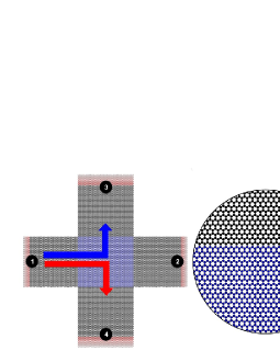
This work is organised as follows. Section II gives the analytical result of the SHA fluctuations. The SHE in graphene is studied in the scope of the Landauer-Büttiker model, which enables us to obtain the universal spin Hall current fluctuations in the CNP. In Section III, we compare the experimental data of SHA found in the literature with our result. In Section IV, we develop the numerical calculations to validate the analytical hypothesis that was presented in Section II. As shown in Fig. 1, the SHE is numerically simulated in a honeycomb lattice sample (blue) that is connected to four terminals. Numerical calculations were implemented using KWANT software Groth et al. (2014). Finally, our conclusions are presented in Section V.
II Spin Hall angle
This section will describe our analysis of the spin Hall current and SHA. We will show that the SHA fluctuations lead to a universal relationship between maximum SHA deviation and dimensionless conductivity. Therefore, we divide this section into two subsections. In the first subsection, we introduce the SHE for a graphene device with disorder connected to four semi-infinite leads that are embedded in the Landauer-Büttiker setup for quantum transport and we then calculate the spin Hall current fluctuation at the CNP. In the second subsection, we develop an analytical calculation of SHA fluctuations.
II.1 Spin Hall current fluctuations
We designed a spin Hall device with four semi-infinite leads (black) connected to a scattering region with disorder and strong SOI (blue), as shown in Fig.(1). The Landauer-Büttiker model can describe the SHE Nikolić, Zârbo, and Souma (2005); Nikolić, B. K. and Zârbo, L. P. (2007); Bardarson, Adagideli, and Jacquod (2007). Therefore, the spin-resolved current through the th electrode is
| (1) |
Applying an electric potential difference between leads 1 and 2, and , leads to a pure longitudinal charge current; see Fig.(1). The spin-up carriers are then deflated to one side of the scattering region, while the spin-down carriers are deflated to the other. This leads to a pure spin Hall current in the transversal direction, see Fig.(1). The transmission coefficients can be obtained from transmission and reflection blocks of the corresponding device scattering -matrix, as follows
| (6) |
where and denote the identity and Pauli matrices, respectively, and with polarisation direction .
Following Refs. Nikolić, Zârbo, and Souma, 2005; Nikolić, B. K. and Zârbo, L. P., 2007; Bardarson, Adagideli, and Jacquod, 2007, we assume that the charge current vanishes in the transverse leads, for and that the charge current is conserved . From Eq. (1), we obtain a general expression for the transversal spin Hall current
| (7) |
where , and also for longitudinal charge current
| (8) | |||||
where . The dimensionless integer is the number of propagating wave modes in the leads, which is proportional to both the lead width () and the Fermi vector () through the equation , while are the potentials of the vertical leads.
Ref. Vasconcelos, Ramos, and Barbosa, 2016 developed an analytic calculation of the spin Hall current average Eq. (7) and its fluctuations for a graphene device at the CNP. However, this was only possible by applying the diagrammatic method Barros et al. (2013); Ramos, Vasconcelos, and Barbosa (2018) of the random matrix theory Beenakker (1997). In this case, the random scattering matrix Eq. (6) is described by the chiral circular symplectic ensemble; that is, class CII in Cartan’s nomenclature Jacquod et al. (2012). This means that the graphene device has a strong SOC, particle-hole and sublattices/mirror symmetries. Assuming uniform SOI, we can obtain the spin Hall current average Vasconcelos, Ramos, and Barbosa (2016) from Eq. (7)
| (9) |
Eq. 9 is in agreement with the result of Ref. Dimitrova, 2005, which has shown that the spin Hall conductivity is null for the uniform Rashba coupling, . Meanwhile, Eq. 9 is not in contradiction to the result of Refs. Dugaev et al., 2010; Raimondi et al., 2012, in which the authors have shown for two different models that the spin Hall conductivity is proportional to the universal constant multiplied by momentum relaxation time and is inversely proportional to the spin relaxation time in the presence of disorder SOI, .
Although the spin Hall current average is null, its fluctuation can be significant because of disorder. From Eq. (7), we obtain that
| (10) |
for a sufficiently large thickness . From Eq. (10), we conclude that the spin Hall current deviation is
| (11) |
which means that the spin Hall current fluctuations of graphene are universals. The longitudinal charge current average of a graphene device in the diffusive regime is appropriately described as McCann and Fal’ko (2012)
| (12) |
in the function of dimensionless longitudinal conductivity .
II.2 Spin Hall angle fluctuations
SHA is defined as the ratio between a transversal spin Hall current and a longitudinal charge current
| (13) |
We must implement the central limit theorem to develop the ensemble average on Eq. (13). Therefore, by taking a sufficiently large thickness , the Eq. (13) can be expanded as
| (14) |
From Eq. (9), we know that the spin Hall current average is null, , which leads us to conclude that
| (15) |
The graphene device that is under study is disordered, which induces fluctuations in the spin Hall current and the longitudinal charge current Qiao et al. (2008); Choe and Chang (2015); Sá, Barbosa, and Ramos (2020). Therefore, it is reasonable that the SHA fluctuates. In the usual way, we define the SHA deviation as
We follow the same methodology for the ensemble average and obtain
| (16) | |||||
Because the spin Hall current average is null, Eq. (16) simplifies to
| (17) |
From Eq. (17) we can infer the SHA deviation with the knowledge of the spin Hall current fluctuations and the charge current average. Eq. (17) is general, which means that it can be applied in any type of disorder device.
By substituting Eqs.(10) and (12) in Eq.(17), we obtain
| (18) |
Eq.(18) indicates that the SHA attains a maximum deviation. Therefore, we can write it in a more general form, as follows
| (19) |
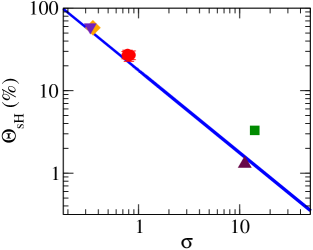
Eq. (19) is valid for a graphene device at the CNP. However, it is the same result obtained by Ref. Santana et al., 2020 for metals. Although the mechanisms of charge-to-spin current conversion in graphene and metals are different, in the presence of strong SOI the random scattering matrices of both devices (6) are distributed by the circular symplectic ensemble of random matrix theory. Therefore, Eq. (19) is a universal relation (i.e., independent of the microscopic features of the material).
III Comparison between theoretical and experimental results
Fig.(2) shows as a function of dimensionless conductivity . The diamond symbol (orange) denotes experimental data of SHA at the CNP of graphene, which was obtained from Ref. Balakrishnan et al., 2013. The dimensionless conductivity axis of the experiment was normalised as cm cm.
The circle symbols (red) of Fig.(2) are obtained from Figs. (12) and (13) between meV in the Supplemental Material of Ref. Balakrishnan et al., 2014 for copper-chemical vapour deposition graphene samples at room temperature.
The triangle up symbol (purple) of Fig.(2) denotes experimental data obtained from Ref. Zhao et al., 2020 for Weyl semimetal WTe2 with graphene. The triangle down symbol (maroon) denotes experimental data obtained from Ref. Hoque et al., 2020 for a hybrid device of TaTe2 in a van der Waals heterostructure with graphene. The squared symbol (green) denotes experimental data obtained from Ref. Safeer et al., 2019 for Graphene/MoS2 van der Waals heterostructures.
IV Numerical results
To confirm the predictions that Eq. (19) is valid for a graphene device with disorder, we performed numerically accurate real-space simulations of the SHA. Fig. (1) illustrates the device design. We expressed the Hamiltonian as , where describes the usual nearest-neighbor hopping, is the nearest-neighbour hopping term describing the Bychkov-Rashba SOC, which explicitly violates symmetry, and is the on-site potential of carbon atoms in the hexagon hosting adatoms, which simulates a charge modulation that is induced locally around the adatom. In terms of annihilation (creation) operators () that remove (add) electrons to site with spin , the terms , and read as follows Milletarì et al. (2017); Gmitra et al. (2016); Cysne, Ferreira, and Rappoport (2018); Barbosa, Ramos, and Ferreira (2021)
| (20) | |||||
| (21) | |||||
| (22) |
where the indices and run over all lattice sites, denotes a sum over nearest-neighbor sites, is the unit vector along the line segment connecting the sites and , and eV is the hopping integral. Therefore, is the Bychkov-Rashba coupling strength between sites and . The disorder is an electrostatic potential that varies randomly from site to site according to a uniform distribution in the interval , where is the disorder strength. The Fermi energy, disorder strength and Bychkov-Rashba SOC values are given in unities of , while the width and length of the device are given in unities of the graphene lattice constant, . All of the numerical results were obtained from 15,000 disorder realisations. The numerical calculations were implemented in KWANT software Groth et al. (2014).
We have developed numerical calculations for two different configurations. The first configuration is for a graphene device with uniform Bychkov-Rashba SOC, where we keep fixed the SOC strength , while the disorder is a random electrostatic potential (as discussed above). The second configuration is for a graphene device with a random Bychkov-Rashba SOC, where the SOC strength is randomly accorded by a uniform distribution in the interval , while the disorder strength is kept null .
IV.1 Uniform Bychkov-Rashba SOC
In this section, we study the SHE with uniform Bychkov-Rashba SOC. The SOC strength of Eq. (21) is fixed and the disorder of the graphene device is introduced by an electrostatic potential , which varies randomly from site to site according to a uniform distribution in the interval , where is the disorder strength.
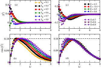
We begin with Fig. (3), which shows numerical calculations of the spin Hall current as a function of disorder from Eq.(7). Figs.(3.a,c) show the spin Hall current average, while Figs.(3.b,d) show its deviation for different values of and Fermi energy. In the former, we observe oscillations in the tails of the spin Hall current average, which are similar to those observed in the numeric results for the diffusive device in Ref. Santana et al., 2020. The underlying mechanism of the oscillations are the fluctuations in potentials . In Figs.(3.a,b), the energy was fixed in for different SOI values . For all values of , the spin Hall current deviation holds the universal maximum deviations Eq. (11) (dashed line), Fig. (3.b). Furthermore, in Figs.(3.c,d), the SOI value was fixed in for different energy values. The spin Hall current has its universal maximum deviation for all energies; see Fig. (3.d).
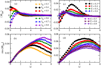
As developed earlier for the spin Hall current, we numerically calculate the longitudinal charge current, Eq.(8), which is depicted in Fig.(4). Figs.(4.a,c) show the charge current average as a function of for different values of and energy, respectively, while Figs.(4.b,d) are their respective deviations. Although the spin Hall current average shows oscillations in the tails, as depicted in Figs.(3.a,c), the charge current average does not present them, as depicted in Figs.(4.a,c). Furthermore, the charge current maximum deviation in Fig.(4.b) occurs for disorder strength values () that are larger than spin Hall maximum deviation (), see Fig.(3.b). From the numeric data of Figs.(4.b,d), we estimate the charge current maximum deviation as (dashed line).
We are now ready to analyse the SHA, Eq.(13), which is depicted in Fig.(5). Figs.(5.a,c) show the SHA average as a function of for different values of and energy, respectively, while Figs.(5.b,d) are their respective deviations. As we can see in Figs.(5.a,c), the SHA average keeps the oscillations present in the spin Hall current average. However, the SHA maximum deviations happen only for , see Fig.(5.b). This means that the efficiency increase is not related to an increase in the spin Hall current fluctuations but is related to an increase in the charge current fluctuations. The charge-to-spin current conversion is more efficient when the charge current fluctuates more, which is in accordance with Eq.(18).
Although Figs. (3.d) and (4.d) show an increase in the maximum deviation of spin and charge currents as a function of energy with converging to a finite value, the maximum SHA deviation decreases as a function of energy without converging; as demonstrated in Fig.(5.d). For example, the SHA has its maximum deviation when the energy is . This means that the SHA decreases as the energy increases, which is in agreement with Eq. (18).
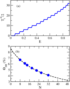
Finally, we are now in a position to connect the numerical results with Eq. (18). Fig. (6.a) shows the transmission coefficient as a function of energy, which gives the relationship between and . Fig. (6.b) shows the maximum SHA deviation from Fig. (5.d) as a function of . The dashed line is the numerical data fit,
Taking the limit of large thickness for which Eq. (18) is valid, it goes to
By comparing the latter with the Eq.(19), we obtain , which drives to a universal relation
(as previously stated). Furthermore, we can estimate the mean free electron path of a graphene device as .
IV.2 Random Bychkov-Rashba SOC
Motivated by Refs. Moca, Marinescu, and Filip, 2008; Dugaev et al., 2010; Raimondi et al., 2012; Kudła et al., 2018; Seibold et al., 2017; Kumar Sharma, Sil, and Chatterjee, 2021; Dugaev, Sherman, and Barnaś, 2011, we analysed the SHE with random Bychkov-Rashba SOC. In this case, the SOC parameter of Eq. (21) is responsible for graphene disorder and is distributed randomly according to a uniform distribution in the interval , where is the SOC strength. Hence, we keep the amplitude of the random electrostatic potential null in the numeric calculation, in Eq. (22).
The random Bychkov-Rashba SOC Hamiltonian (21) is similar to the one that was introduced by Ref. Dugaev, Sherman, and Barnaś, 2011 in the small correlation length limit. In this limit, the Dyakonov-Perel’ mechanism dominates the spin fluctuating precession in the graphene device; that is, the electron spin interacts with the local rather than with the rapidly changing random spin-orbit field Dugaev, Sherman, and Barnaś (2011).
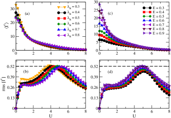
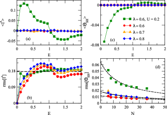
Figs. (7.a) and (7.c) show the numeric calculation data for the average of the spin Hall current and SHA as a function of energy, respectively. For a direct comparison between uniform and random SOC, we plotted a uniform SOC numeric data, with and (square symbols), and three different numeric data for random SOC, with SOC strengths , 0.7 and 0.8. The former has a no null spin Hall current average, while the latter has a null average for all energy ranges, see Fig. (7.a). Similar behavior is found for the SHA average, see Fig. (7.c). However, we are interested in the spin Hall current and SHA deviations.
Fig. (7.b) shows the spin Hall current deviation as an energy function. The numerical data of uniform and random SOC go to 0.18 as the energy increases, which is in agreement with Eq. (11). Therefore, the universal spin Hall current fluctuations are significant for both cases. This indicates that vanishing SHE is irrelevant for realistic finite-size systems, where self-averaging over an infinite system size is avoided.
Finally, we plotted the maximum SHA deviation as a function of thickness in Fig. (7.d). From this figure it can be seen that for uniform and random SOC, maximum SHA deviation decreases with thickness increases , which is in agreement with our analytical result Eq. (18). Therefore, the numeric data can be well fitted by relation .
V Conclusions
This work studied the SHA fluctuations of single-layer graphene with disorder and strong SOC. We analytically show that the product between maximum SHA deviation and dimensionless conductivity of a graphene device follows the same universal relation of metals, see Eq. (19). To confirm this analytical result, we developed numerically exact real-space simulations from the tight-binding model with Bychkov-Rashba SOC. The numeric data are consistent with Eq. (19), which confirms its validity to Dirac materials as graphene.
We also developed numerical simulations of SHE in the presence of uniform and random Bychkov-Rashba SOC. We found that the averages of spin Hall current and SHA as an energy function have different behaviors for uniform and random SOC—the former has a finite value for the spin Hall current and SHA averages, while the latter has a null average; see Figs. (7.a) and (7.b).
Although the averages of spin Hall current and SHA have different behaviors for uniform and random SOC, their deviations are large and equivalent; as shown in Figs. (7.b) and (7.d). This confirms that vanishing SHE is irrelevant for a realistic finite-size graphene device where self-averaging over an infinite system size is avoided. Therefore, the maximum SHA deviation of the graphene devices with uniform or random SOC follows Eq. (19).
Finally, we confronted five different experimental data Balakrishnan et al. (2013, 2014); Zhao et al. (2020); Hoque et al. (2020); Safeer et al. (2019) with Eq. (19). As shown in Fig. (2), both the analytical results and the experimental data agree satisfactorily. Therefore, we believe that our results can contribute to a more profound understanding of SHE and SHA fluctuation in Dirac materials.
Acknowledgments
This work was supported by CNPq (Conselho Nacional de Desenvolvimento Científico e Tecnológico) and FACEPE (Fundação de Amparo à Ciência e Tecnologia do Estado de Pernambuco).
Data Availability
The data that support the findings of this study are available from the corresponding author upon reasonable request.
References
References
- Datta and Das (1990) S. Datta and B. Das, Applied Physics Letters 56, 665 (1990).
- Sayed et al. (2021) S. Sayed, S. Hong, X. Huang, L. Caretta, A. S. Everhardt, R. Ramesh, S. Salahuddin, and S. Datta, Phys. Rev. Applied 15, 054004 (2021).
- Jedema et al. (2003) F. J. Jedema, M. S. Nijboer, A. T. Filip, and B. J. van Wees, Phys. Rev. B 67, 085319 (2003).
- Lou et al. (2007) X. Lou, C. Adelmann, S. Crooker, E. Garlid, J. Zhang, S. Reddy, S. Flexner, C. Palmstrøm, and P. Crowell, Nature Physics 3, 197 (2007).
- Hirohata and Takanashi (2014) A. Hirohata and K. Takanashi, Journal of Physics D: Applied Physics 47, 193001 (2014).
- Wang, Alzate, and Amiri (2013) K. L. Wang, J. G. Alzate, and P. K. Amiri, Journal of Physics D: Applied Physics 46, 074003 (2013).
- Hirsch (1999) J. E. Hirsch, Phys. Rev. Lett. 83, 1834 (1999).
- Dyakonov and Perel (1971a) M. Dyakonov and V. Perel, Soviet Journal of Experimental and Theoretical Physics Letters 13, 467 (1971a).
- Dyakonov and Perel (1971b) M. Dyakonov and V. Perel, Physics Letters A A 35, 459 (1971b).
- Schliemann (2006) J. Schliemann, International Journal of Modern Physics B 20, 1015 (2006).
- Sinova et al. (2015) J. Sinova, S. O. Valenzuela, J. Wunderlich, C. H. Back, and T. Jungwirth, Rev. Mod. Phys. 87, 1213 (2015).
- Seifert et al. (2018) T. S. Seifert, N. M. Tran, O. Gueckstock, S. M. Rouzegar, L. Nadvornik, S. Jaiswal, G. Jakob, V. V. Temnov, M. Münzenberg, M. Wolf, M. Kläui, and T. Kampfrath, Journal of Physics D: Applied Physics 51, 364003 (2018).
- Wang et al. (2015) Z. Wang, W. Zhao, E. Deng, J.-O. Klein, and C. Chappert, Journal of Physics D: Applied Physics 48, 065001 (2015).
- Ando and Saitoh (2012) K. Ando and E. Saitoh, Nature Communications 3 (2012).
- Althammer et al. (2013) M. Althammer, S. Meyer, H. Nakayama, M. Schreier, S. Altmannshofer, M. Weiler, H. Huebl, S. Geprägs, M. Opel, R. Gross, D. Meier, C. Klewe, T. Kuschel, J.-M. Schmalhorst, G. Reiss, L. Shen, A. Gupta, Y.-T. Chen, G. E. W. Bauer, E. Saitoh, and S. T. B. Goennenwein, Phys. Rev. B 87, 224401 (2013).
- Sagasta et al. (2016) E. Sagasta, Y. Omori, M. Isasa, M. Gradhand, L. E. Hueso, Y. Niimi, Y. Otani, and F. Casanova, Phys. Rev. B 94, 060412 (2016).
- Fritz et al. (2018) K. Fritz, S. Wimmer, H. Ebert, and M. Meinert, Phys. Rev. B 98, 094433 (2018).
- Pai et al. (2012) C.-F. Pai, L. Liu, Y. Li, H.-W. Tseng, D. Ralph, and R. Buhrman, Applied Physics Letters 101 (2012).
- Lou et al. (2020) P. C. Lou, A. Katailiha, R. G. Bhardwaj, T. Bhowmick, W. P. Beyermann, R. K. Lake, and S. Kumar, Phys. Rev. B 101, 094435 (2020).
- Okano et al. (2019) G. Okano, M. Matsuo, Y. Ohnuma, S. Maekawa, and Y. Nozaki, Phys. Rev. Lett. 122, 217701 (2019).
- Zhu, Ralph, and Buhrman (2018) L. Zhu, D. C. Ralph, and R. A. Buhrman, Phys. Rev. Applied 10, 031001 (2018).
- Wang et al. (2014) H. L. Wang, C. H. Du, Y. Pu, R. Adur, P. C. Hammel, and F. Y. Yang, Phys. Rev. Lett. 112, 197201 (2014).
- Alves-Santos et al. (2017) O. Alves-Santos, E. F. Silva, M. Gamino, R. O. Cunha, J. B. S. Mendes, R. L. Rodríguez-Suárez, S. M. Rezende, and A. Azevedo, Phys. Rev. B 96, 060408 (2017).
- Alves Santos et al. (2019) O. Alves Santos, E. Silva, M. Gamino, J. Mendes, S. Rezende, and A. Azevedo, AIP Advances 9, 035025 (2019).
- Zhang et al. (2015) W. Zhang, W. Han, X. Jiang, S.-H. Yang, and S. S. P. Parkin, Nature Physics 11, 496–502 (2015).
- Nikolić, Zârbo, and Souma (2005) B. K. Nikolić, L. P. Zârbo, and S. Souma, Phys. Rev. B 72, 075361 (2005).
- Nikolić, B. K. and Zârbo, L. P. (2007) Nikolić, B. K. and Zârbo, L. P., EPL 77, 47004 (2007).
- Ren et al. (2006) W. Ren, Z. Qiao, J. Wang, Q. Sun, and H. Guo, Phys. Rev. Lett. 97, 066603 (2006).
- Bardarson, Adagideli, and Jacquod (2007) J. H. Bardarson, i. d. I. Adagideli, and P. Jacquod, Phys. Rev. Lett. 98, 196601 (2007).
- Qiao et al. (2008) Z. Qiao, J. Wang, Y. Wei, and H. Guo, Phys. Rev. Lett. 101, 016804 (2008).
- Ramos et al. (2012) J. G. G. S. Ramos, A. L. R. Barbosa, D. Bazeia, M. S. Hussein, and C. H. Lewenkopf, Phys. Rev. B 86, 235112 (2012).
- Vasconcelos, Ramos, and Barbosa (2016) T. C. Vasconcelos, J. G. G. S. Ramos, and A. L. R. Barbosa, Phys. Rev. B 93, 115120 (2016).
- Beenakker (1997) C. W. J. Beenakker, Rev. Mod. Phys. 69, 731 (1997).
- Santana et al. (2020) F. A. F. Santana, J. M. da Silva, T. C. Vasconcelos, J. G. G. S. Ramos, and A. L. R. Barbosa, Phys. Rev. B 102, 041107 (2020).
- Inoue, Bauer, and Molenkamp (2004) J.-i. Inoue, G. E. W. Bauer, and L. W. Molenkamp, Phys. Rev. B 70, 041303 (2004).
- Raimondi and Schwab (2005) R. Raimondi and P. Schwab, Phys. Rev. B 71, 033311 (2005).
- Dimitrova (2005) O. V. Dimitrova, Phys. Rev. B 71, 245327 (2005).
- Khaetskii (2006) A. Khaetskii, Phys. Rev. Lett. 96, 056602 (2006).
- Milletarì et al. (2017) M. Milletarì, M. Offidani, A. Ferreira, and R. Raimondi, Phys. Rev. Lett. 119, 246801 (2017).
- Novoselov et al. (2004) K. Novoselov, A. Geim, S. Morozov, D. Jiang, Y. Zhang, S. Dubonos, I. Grigorieva, and A. Firsov, Nat. Mater. 6 (2004).
- Geim and Novoselov (2007) A. Geim and K. Novoselov, Nature materials 6, 183 (2007).
- Castro Neto et al. (2009) A. H. Castro Neto, F. Guinea, N. M. R. Peres, K. S. Novoselov, and A. K. Geim, Rev. Mod. Phys. 81, 109 (2009).
- Avsar et al. (2020) A. Avsar, H. Ochoa, F. Guinea, B. Özyilmaz, B. J. van Wees, and I. J. Vera-Marun, Rev. Mod. Phys. 92, 021003 (2020).
- Ingla-Aynés et al. (2015) J. Ingla-Aynés, M. H. D. Guimarães, R. J. Meijerink, P. J. Zomer, and B. J. van Wees, Phys. Rev. B 92, 201410 (2015).
- Garcia et al. (2018) J. H. Garcia, M. Vila, A. W. Cummings, and S. Roche, Chem. Soc. Rev. 47, 3359 (2018).
- Schubert, Schleede, and Fehske (2009) G. Schubert, J. Schleede, and H. Fehske, Phys. Rev. B 79, 235116 (2009).
- Wang and Wu (2015) Y.-X. Wang and Y.-M. Wu, Physica B: Condensed Matter 478 (2015).
- Islam and Benjamin (2016) S. F. Islam and C. Benjamin, Carbon 110, 304 (2016).
- Balakrishnan et al. (2013) J. Balakrishnan, G. Kok Wai Koon, M. Jaiswal, A. H. Castro Neto, and B. Ozyilmaz, Nature Physics 9, 284 (2013).
- Balakrishnan et al. (2014) J. Balakrishnan, G. K. W. Koon, A. Avsar, Y. Ho, J. H. Lee, M. Jaiswal, S.-J. Baeck, J.-H. Ahn, A. Ferreira, M. A. Cazalilla, A. H. C. Neto, and B. Ozyilmaz, Nature Communications 102, 4748 (2014).
- Zhao et al. (2020) B. Zhao, D. Khokhriakov, Y. Zhang, H. Fu, B. Karpiak, A. M. Hoque, X. Xu, Y. Jiang, B. Yan, and S. P. Dash, Phys. Rev. Research 2, 013286 (2020).
- Hoque et al. (2020) A. M. Hoque, D. Khokhriakov, B. Karpiak, and S. P. Dash, Phys. Rev. Research 2, 033204 (2020).
- Safeer et al. (2019) C. K. Safeer, J. Ingla-Aynés, F. Herling, J. H. Garcia, M. Vila, N. Ontoso, M. R. Calvo, S. Roche, L. E. Hueso, and F. Casanova, Nano Letters 19, 1074 (2019).
- Wu et al. (2020) Y. Wu, L. Sheng, L. Xie, S. Li, P. Nie, Y. Chen, X. Zhou, and X. Ling, Carbon 166, 396 (2020).
- Gmitra et al. (2016) M. Gmitra, D. Kochan, P. Högl, and J. Fabian, Phys. Rev. B 93, 155104 (2016).
- Cysne, Ferreira, and Rappoport (2018) T. P. Cysne, A. Ferreira, and T. G. Rappoport, Phys. Rev. B 98, 045407 (2018).
- Barbosa, Ramos, and Ferreira (2021) A. L. R. Barbosa, J. G. G. S. Ramos, and A. Ferreira, Phys. Rev. B 103, L081111 (2021).
- Moca, Marinescu, and Filip (2008) C. P. Moca, D. C. Marinescu, and S. Filip, Phys. Rev. B 77, 193302 (2008).
- Dugaev et al. (2010) V. K. Dugaev, M. Inglot, E. Y. Sherman, and J. Barnaś, Phys. Rev. B 82, 121310 (2010).
- Raimondi et al. (2012) R. Raimondi, P. Schwab, C. Gorini, and G. Vignale, Annalen der Physik 524 (2012).
- Kudła et al. (2018) S. Kudła, A. Dyrdał, V. K. Dugaev, E. Y. Sherman, and J. Barnaś, Phys. Rev. B 97, 245307 (2018).
- Seibold et al. (2017) G. Seibold, S. Caprara, M. Grilli, and R. Raimondi, Journal of Magnetism and Magnetic Materials 440, 63 (2017).
- Kumar Sharma, Sil, and Chatterjee (2021) H. Kumar Sharma, S. Sil, and A. Chatterjee, Journal of Magnetism and Magnetic Materials 529, 167711 (2021).
- Dugaev, Sherman, and Barnaś (2011) V. K. Dugaev, E. Y. Sherman, and J. Barnaś, Phys. Rev. B 83, 085306 (2011).
- Groth et al. (2014) C. W. Groth, M. Wimmer, A. R. Akhmerov, and X. Waintal, New Journal of Physics 16, 063065 (2014).
- Barros et al. (2013) M. S. M. Barros, A. J. N. Júnior, A. F. Macedo-Junior, J. G. G. S. Ramos, and A. L. R. Barbosa, Phys. Rev. B 88, 245133 (2013).
- Ramos, Vasconcelos, and Barbosa (2018) J. G. G. S. Ramos, T. C. Vasconcelos, and A. L. R. Barbosa, Journal of Applied Physics 123, 034304 (2018).
- Jacquod et al. (2012) P. Jacquod, R. S. Whitney, J. Meair, and M. Büttiker, Phys. Rev. B 86, 155118 (2012).
- McCann and Fal’ko (2012) E. McCann and V. I. Fal’ko, Phys. Rev. Lett. 108, 166606 (2012).
- Choe and Chang (2015) D.-H. Choe and K. J. Chang, Scientific Reports 5, 10997 (2015).
- Sá, Barbosa, and Ramos (2020) L. G. C. S. Sá, A. L. R. Barbosa, and J. G. G. S. Ramos, Phys. Rev. B 102, 115105 (2020).