Identification of exciton complexes in a charge-tuneable Janus W monolayer
Abstract
Janus transition-metal dichalcogenide monolayers are fully artificial materials, where one plane of chalcogen atoms is replaced by chalcogen atoms of a different type. Theory predicts an in-built out-of-plane electric field, giving rise to long-lived, dipolar excitons, while preserving direct-bandgap optical transitions in a uniform potential landscape. Previous Janus studies had broad photoluminescence (15 meV) spectra obfuscating their excitonic origin. Here, we identify the neutral, and negatively charged inter- and intravalley exciton transitions in Janus W monolayer with 6 meV optical linewidths. We combine a recently developed synthesis technique, with the integration of Janus monolayers into vertical heterostructures, allowing doping control. Further, magneto-optic measurements indicate that monolayer W has a direct bandgap at the K points. This work provides the foundation for applications such as nanoscale sensing, which relies on resolving excitonic energy shifts, and photo-voltaic energy harvesting, which requires efficient creation of long-lived excitons and integration into vertical heterostructures.
Layered materials are solids with strong intralayer bonds but only weak van der Waals coupling between layers [1]. These materials have a range of electronic [2], optical [3], and topological [4] properties and can be combined in vertical heterostructures with pristine atomic interfaces despite mismatched lattice parameters [5, 6, 7, 8]. Direct-bandgap semiconducting transition-metal dichalcogenide (TMD) monolayers are a class of layered material, which are particularly interesting due to their opto-electronic properties [9, 10, 11, 12]. Optical excitation creates excitons, i.e. bound electron-hole pairs, at the K and K’ direct-bandgap edges [13, 14], while the strong spin-orbit interaction and broken inversion symmetry leads to coupling of the spin and valley degrees of freedom [15]. Heterostructures comprising two different TMD monolayers can have a type-II band alignment [16, 17], which localises electrons in one monolayer and holes in the other [18]. This charge separation results in excitons with a permanent electric dipole moment [19] and long lifetime (up to 0.2 ms) [20], due to a reduced overlap of electron and hole wavefunctions [21]. While such stacking configurations enable tuneability with layer angle and introduces emergent moiré physics [22], they are also susceptible to an inhomogeneous potential landscape due to spatial variations in layer separation and twist angle [23, 24].
Janus TMDs (J-TMD) are a new class of layered materials, first explored theoretically in 2013 [25], that promise Rashba splitting [26, 27]; piezoelectric response [28, 29]; and long-lived, dipolar excitons [30] in an intrinsically uniform potential landscape. To form a Janus monolayer, a conventional monolayer TMD, such as WSe2, is altered to create W with Se atoms on one face and S atoms on the other, effectively placing a WSe2/WS2 interface within the monolayer. This artificially modified atomic ordering breaks the out-of-plane crystal symmetry and results in an in-built electric field [31], which separates the electron and hole wavefunctions and generates excitons with a permanent electric dipole [32]. Janus monolayers were first experimentally realised in 2017 [33, 34]; however, the excitonic origin of the optical transitions in J-TMDs has still not been clarified. One challenge is the broad 18-meV photoluminescence (PL) lineshape for the narrowest reported emission in J-TMDs, achieved via hexagonal boron nitride (hBN) encapsulation [35]. The second challenge is the absence, to-date, of integration of J-TMDs into electrically gated devices.
In this work, we report the identification of the neutral exciton (X0), the negative inter- and intravalley trions (X and X, respectively) and the X-′ transition in a Janus W monolayer by using reflectance contrast (RC) and PL spectroscopy. We confirm the Janus conversion of a monolayer exfoliated from flux-grown WSe2 bulk crystal via Raman and PL spectroscopy over the flake. By encapsulating monolayer W in hBN, we are able to measure the narrowest Janus emission (5.9 meV linewidth) reported. Charge-state control via direct contacting with graphene further enables identification of the negatively charged excitonic species. Furthermore, we measure the X0 g factor to be 4, consistent with conventional TMDs. By establishing the excitonic origins of the spectral features in this material, we provide the basis for future work that will explore the novel properties of J-TMDs.
Device characterisation
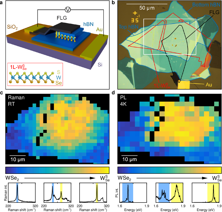
Figure 1a is an illustration of one of our Janus devices. The silicon (Si) substrate is used as a back gate, separated from the Janus monolayer by SiO2 and multilayer hBN (ML-hBN). A parent WSe2 monolayer (1L-WSe2) is exfoliated onto the ML-hBN. The 1L-WSe2 is then converted into a Janus W monolayer (1L-W), with Se atoms on the bottom and S atoms on the top, by following a room-temperature in-situ conversion technique (see Methods and Supplementary Notes S1, S2) [36, 37]. An additional ML-hBN transferred on top of the converted 1L-W encapsulates the flake, and a top gate comprised of few-layer graphene (FLG) electrically contacts the 1L-W. Figure 1b shows an optical microscope image of the device, where the 1L-W is outlined in red, the bottom and top hBN in blue, and the FLG in black.
Figure 1c shows a Raman spectroscopy map of the device, acquired at room temperature using 2.33 eV optical excitation, in the region highlighted by the white box in Fig. 1b. The colour code indicates the relative intensity between the characteristic 1L-WSe2 + Raman mode (blue) [38] and the Janus 1L-W Raman mode (yellow) [39], with representative Raman spectra from regions with different degrees of Janus conversion shown below the Raman map (see S3). The Raman spectra from the large region ( 400 m2) of fully converted Janus 1L-W evidence that the converted region is ordered Janus 1L-W [39] rather than a disordered alloy, which would show the representative Raman peaks of 1L-WSe2 and 1L-WS2 [40, 36].
Figure 1d shows a PL map, acquired at 4 K using 2.33 eV optical excitation, in the same region of the device as in Fig. 1c. Similar to Fig. 1c, the colour code shows the relative PL emission intensity between the distinct 1L-WSe2 (blue) and Janus 1L-W (yellow) spectral bands [36, 41]. The PL map displays strong correlation with the Raman map in Fig. 1c, which validates our assignment of the Janus 1L-W spectral band. Therefore, we focus on the exciton emission in the spatial region of full Janus conversion.
Identification of the neutral exciton
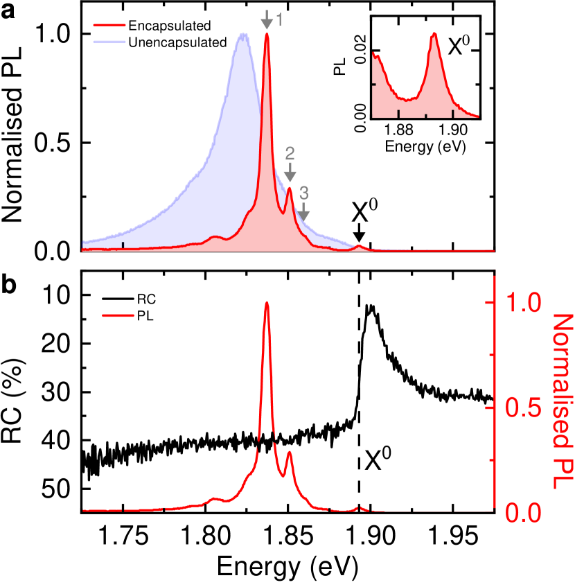
Encapsulation in hBN reduces the linewidths of PL peaks in conventional 1L-TMDs [42, 43, 44], thus allowing for the identification of excitonic species [45, 46]. Figure 2a compares a representative PL spectrum at 4 K from our ML-hBN encapsulated 1L-W device (red curve) to the spectrum from unencapsulated 1L-W on a Si/SiO2 substrate (blue curve). The unencapsulated 1L-W has a broad spectrum, with a full width at half maximum (FWHM) on the order 30 meV, on par with the narrowest linewidth reported to-date for unencapsulated Janus TMDs [37]. In contrast, encapsulation with hBN allows us to resolve multiple spectral features with significantly reduced linewidths (10 meV).
The peaks labelled 1, 2, 3 and X0 are present in the 1L-W PL spectra across the whole device (see S3), indicating that these arise from intrinsic excitonic transitions. Since the highest-energy PL peak in both 1L-WSe2 and 1L-WS2 stems from neutral excitons [42], the peak at 1.893 eV is a likely candidate for the neutral exciton, X0, in 1L-W. To verify this, we directly probe excitonic absorption resonances using RC spectroscopy (see Methods) [14].
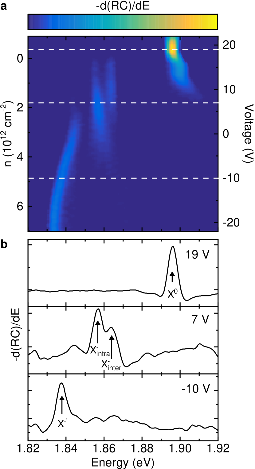
Figure 2b shows a RC spectrum from our 1L-W device (black curve) and the PL spectrum from the same location (red curve). The RC signal shows a strong feature at 1.893 eV, which confirms our assignment of X0. The lowest observed PL FWHM of the Janus X0 transition is 5.9 meV in our device, the lowest reported to date. The X0 transition is present in both PL and RC across the fully converted Janus region (see S3), with an average PL transition energy of 1.890(1) eV and an average FWHM of 8.4(4) meV.
Power-dependent PL measurements (see S4) provide further evidence that X0 is the neutral exciton transition as its intensity scales linearly with power over the measured range 15 nW to 50 W (corresponding to 3 Wcm-2 to 104 Wcm-2). We note that in the spectral range 1.750 to 1.825 eV we also observe PL peaks with linear power dependences at low power and that saturate in the range 50 to 500 nW (10 to 100 Wcm-2). This power saturation suggests the presence of localised defects displaying quantum light emission [47, 48, 20].
Density functional theory (DFT) calculations of the 1L-W band structure (see S5) show that, similar to conventional tungsten-based TMDs (1L-WSe2 and 1L-WS2) [49, 50, 51], 1L-W is direct-bandgap at the K points, with a spin ordering such that the upper valence band is opposite in spin to the lower spin-split conduction band. The spin ordering in the conduction band allows for both a negatively charged intervalley trion (X), with the two electrons in different valleys, and an intravalley trion (X), with the two electrons in the same valley. Our DFT calculations predict the transition energies of the Coulomb-exchange split X and X to be 26 meV and 32 meV, respectively, below the transition energy of the neutral exciton in free-standing 1L-W.
Voltage-controlled generation of charged excitons
To measure the charged excitonic transitions of 1L-W, we tune its doping by applying a voltage between the 1L-W and the Si substrate. Figure 3a shows the RC derivative signal as we vary the doping density, (Methods). Similar doping dependence is observed on a second device (see S2). In the operational range of voltages, only the -doped regime is accessible, due to an intrinsic -doping of cm-2. The previously identified X0 transition, here at 1.896 eV, dominates the RC signal between +21 to +17 V, corresponding to charge neutrality. As we decrease the voltage, and -dope the 1L-W, lower energy transitions appear, which are analogous to the transitions observed in the -doped regime for WSe2 [52, 53, 54].
Figure 3b presents the RC derivative at 19, 7 and V. The neutral exciton, X0, is shown in the line cut at 19 V. Between +17 to +5 V, we see a doublet, which we identify as X and X in the line cut at 7 V with peaks at 1.864 eV and 1.857 eV (32 meV and 39 meV below X0 respectively). We attribute the difference in energies of these trions compared to the DFT calculation to a difference in dielectric environment caused by ML-hBN encapsulation. The exchange splitting between the negative trion transitions of 7 meV is in good agreement with our calculations.
At increased -doping, below 5 V, the X and X peaks vanish and a single peak, labelled X-′ in the linecut at -10 V in Fig. 3b, dominates the derivative of the RC spectrum. The X-′ peak initially appears at 1.845 eV and redshifts by 10 meV between +5 and -17 V. An excitonic transition with a similar doping dependence has previously been observed in 1L-WSe2 [53, 54, 55] and attributed to neutral excitons bound to intervalley plasmons [56, 55]. We expect this peak in 1L-W to be similar in origin.
Magnetic-field dependence of Janus excitons
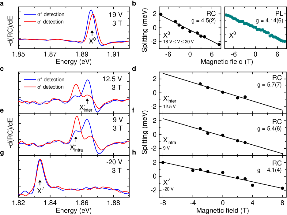
We next probe the exciton g factors by applying an out-of-plane magnetic field, , and measuring the Zeeman energy splitting of the exciton transitions. We send unpolarised light to the device and detect the RC spectra with both and circular polarisations. The left-aligned panels (a, c, e and g) in Fig. 4 display the RC derivative spectra for each excitonic transition measured at 3 T magnetic field, with the right-circular () and left-circular () polarisations shown by the blue and red curves, respectively. The splitting as a function of is shown in the right-hand panels (b, d, f and h) of Fig. 4. Linear fits give the magnitude of the exciton transition g factors, where ( = 58 eV T-1 is the Bohr magneton).
Figure 4a presents the RC derivative spectra for X0 at 3 T, showing a well-resolved splitting. Figure 4b shows for X0 as a function of magnetic field, for both RC and PL. From the linear fit we extract similar g factors of 4.5(2) and 4.14(6) for RC and PL, respectively. For conventional TMDs, g factors with values of 4 have typically been assigned to bright excitons in the K and K’ valleys, with valley, orbital and spin contributing to the magnetic moment [57, 58]. The measured g factors are consistent with 1L-W having a direct-bandgap at the K points.
The g factors of the negatively charged trions depend strongly on doping, ranging from 3-13 for voltages from 8 to 14 V (see S6). For conventional TMDs, this dependence has been attributed to many-body interactions with the Fermi sea of electrons [59, 60]. Figure 4c-f shows RC derivative spectra and splittings as a function of magnetic field for the negative trions at example voltages. We find a g factor of 5.7(7) for X and 5.4(6) for X at the voltages presented. The X and X transitions additionally show evidence of the thermalisation of the excess charge, as observed in conventional tungsten-based TMDs [58, 45, 61]. Beyond 3 T, this leads to only a single polarisation being observable for each negative trion.
Figure 4g shows the polarisation-resolved RC derivative spectrum for the X-′ transition at 3 T. Fig. 4h displays the RC splitting of X-′ as a function of magnetic field, which gives a g factor of 4.1(4), consistent with the interpretation of X-′ as the neutral exciton dressed by many-body interactions [53, 54, 55].
Conclusions
We have identified several excitonic complexes in Janus 1L-W: X0, X, X and X-′ and measured their g factors by integrating a hBN encapsulated 1L-W into a charge-control device. Integrating J-TMDs into vertical heterostructures is key to designing photovoltaics [62, 63], while resolving few-meV exciton linewidths and identifying the exciton spectrum determines the suitability of J-TMDs for sensing [64, 65]. Future work includes identifying the transitions that give rise to the as-yet unidentified PL peaks as well as measuring the excitonic spectrum in the positively doped regime. An immediate next step is measuring the out-of-plane electric dipole moment of excitons in 1L-W by applying an out-of-plane electric field in a capacitor-like device structure. The predicted permanent electric dipole moment of 0.24 D [31] for the Janus X0, means that the resulting Stark shift of 5 meV at 1 V/nm would be resolved with our 6 meV linewidths.
Acknowledgements
We acknowledge funding from the EU Quantum Technology (2D-SIPC) and Graphene Flagships; EU grants CHARM and Graph-X; ERC grants PEGASOS, Hetero2D and GSYNCOR; and EPSRC Grants EP/K01711X/1, EP/K017144/1, EP/N010345/1 and EP/L016087/1. D. M. K. acknowledges support of a Royal Society university research fellowship URF\R1\180593. S.T. acknowledges primary support from DOE-SC0020653 (materials synthesis), NSF CMMI 1825594 (NMR and TEM studies), NSF DMR-2206987 (magnetic measurements), NSF CMMI-1933214, NSF 1904716, NSF 1935994, NSF ECCS 2052527, DMR 2111812, and CMMI 2129412 (scalability of Janus layers).
Appendix A Fabrication
We build our device by following a multi-step process: first, the bottom ML-hBN is mechanically exfoliated onto a Si/SiO2 (90 nm oxide thickness) substrate. Second, a parent 1L-WSe2 is mechanically exfoliated from a flux-zone grown [66] bulk WSe2 crystal and deposited on top of the bottom ML-hBN by polydimethylsiloxane (PDMS) transfer. Third, the 1L-WSe2 undergoes AFM flattening [67] and subsequent conversion to a Janus 1L-W by using the selective epitaxial atomic replacement (SEAR) method [36], while recording time-resolved Raman spectroscopy measurements in-situ to achieve deterministic conversion [37]. Fourth, the top ML-hBN and FLG are sequentially deposited on top of the 1L-W by PDMS transfer, with annealing to 150 ∘C and AFM flattening after each layer is deposited. The FLG is mechanically exfoliated from graphite sourced from HQ Graphene. Fifth, gold contacts are deposited using standard electron-beam lithography procedures.
AFM topography (Bruker Icon) is used to confirm the layer thicknesses and Raman spectroscopy (Horiba LabRam Evolution) is used to characterise the various constituents of the heterostructure, along with confirming the conversion from 1L-WSe2 to 1L-W (see S1).
Appendix B Optical measurements
All 4 K measurements were taken in a closed-cycle cryostat (AttoDRY 1000 from Attocube Systems AG), equipped with an 8 T superconducting magnet.
Excitation and collection light pass through a home-built confocal microscope in reflection geometry, with a 0.81 numerical aperture apochromatic objective (LT-APO/NIR/0.81 from Attocube Systems AG). The PL measurements use continuous-wave excitation from a 2.33 eV laser (Ventus 532 from Laser Quantum Ltd.), with the reported excitation powers measured on the sample and the optical intensity calculated from the optical spot size given by the 0.81 NA. The PL signal is sent to a 150-line grating spectrometer (Princeton Instruments Inc.).
The RC measurements use broadband light (Thorlabs mounted LED M660L4, nominal wavelength 660 nm, FWHM 20 nm). The reflected light is collected in the confocal microscope discussed above and the spectra are recorded on the same 150-line grating spectrometer as for PL. RC is calculated by comparing the spectrum reflected from the heterostructure in a region with the 1L-W, , and without 1L-W, . RC as a function of emission energy is then given by
Appendix C Gate-voltage to layer-doping conversion
The doping density (charge per unit area) is calculated from the applied voltage (Keithley 2400 SMU), by using the gate capacitance,
The intrinsic doping, , is the doping density at zero applied voltage and the magnitude of the electron charge is C.
The voltage is applied across both the ML-hBN and SiO2 and the gate capacitance can be derived by combining the dielectric layers of ML-hBN and SiO2 in series
The relative dielectric constant of SiO2 and hBN is [70] and [71], respectively. Fm-1 is the vacuum permittivity.
The thickness of SiO2 is nm and the thickness of hBN is nm (see S1). The intrinsic doping density is cm-2, determined by setting the doping density to when the reflectance contrast signal from the neutral exciton vanishes (17 V) [53], where positive indicates electron doping.
References
- [1] Novoselov, K. S. et al. Two-dimensional atomic crystals. Proceedings of the National Academy of Sciences 102, 10451–10453 (2005).
- [2] Radisavljevic, B., Radenovic, A., Brivio, J., Giacometti, V. & Kis, A. Single-layer MoS2 transistors. Nature Nanotechnology 6, 147–150 (2011).
- [3] Palacios-Berraquero, C. et al. Large-scale quantum-emitter arrays in atomically thin semiconductors. Nature Communications 8, 1–6 (2017).
- [4] Kou, L., Ma, Y., Sun, Z., Heine, T. & Chen, C. Two-dimensional topological insulators: Progress and prospects. The Journal of Physical Chemistry Letters 8, 1905–1919 (2017).
- [5] Bonaccorso, F. et al. Production and processing of graphene and 2d crystals. Materials Today 15, 564–589 (2012).
- [6] Geim, A. K. & Grigorieva, I. V. Van der Waals heterostructures. Nature 499, 419–425 (2013).
- [7] Ferrari, A. C. et al. Science and technology roadmap for graphene, related two-dimensional crystals, and hybrid systems. Nanoscale 7, 4598–4810 (2015).
- [8] Backes, C. et al. Production and processing of graphene and related materials. 2D Materials 7, 022001 (2020).
- [9] Mak, K. F., Lee, C., Hone, J., Shan, J. & Heinz, T. F. Atomically thin MoS2: a new direct-gap semiconductor. Physical Review Letters 105, 136805 (2010).
- [10] Xiao, D., Liu, G.-B., Feng, W., Xu, X. & Yao, W. Coupled spin and valley physics in monolayers of MoS2 and other group-VI dichalcogenides. Physical Review Letters 108, 196802 (2012).
- [11] Jones, A. M. et al. Optical generation of excitonic valley coherence in monolayer WSe2. Nature Nanotechnology 8, 634–638 (2013).
- [12] Koppens, F. et al. Photodetectors based on graphene, other two-dimensional materials and hybrid systems. Nature Nanotechnology 9, 780–793 (2014).
- [13] Zeng, H., Dai, J., Yao, W., Xiao, D. & Cui, X. Valley polarization in MoS2 monolayers by optical pumping. Nature Nanotechnology 7, 490–493 (2012).
- [14] Mak, K. F., He, K., Shan, J. & Heinz, T. F. Control of valley polarization in monolayer MoS2 by optical helicity. Nature Nanotechnology 7, 494–498 (2012).
- [15] Wang, G. et al. Colloquium: Excitons in atomically thin transition metal dichalcogenides. Reviews of Modern Physics 90, 021001 (2018).
- [16] Kang, J., Tongay, S., Zhou, J., Li, J. & Wu, J. Band offsets and heterostructures of two-dimensional semiconductors. Applied Physics Letters 102, 012111 (2013).
- [17] Gong, C. et al. Band alignment of two-dimensional transition metal dichalcogenides: Application in tunnel field effect transistors. Applied Physics Letters 103, 053513 (2013).
- [18] Mak, K. F. & Shan, J. Opportunities and challenges of interlayer exciton control and manipulation. Nature Nanotechnology 13, 974–976 (2018).
- [19] Jauregui, L. A. et al. Electrical control of interlayer exciton dynamics in atomically thin heterostructures. Science 366, 870–875 (2019).
- [20] Montblanch, A. R.-P. et al. Confinement of long-lived interlayer excitons in WS2/WSe2 heterostructures. Communications Physics 4, 119 (2021).
- [21] Jiang, Y., Chen, S., Zheng, W., Zheng, B. & Pan, A. Interlayer exciton formation, relaxation, and transport in TMD van der Waals heterostructures. Light: Science & Applications 10, 1–29 (2021).
- [22] Huang, D., Choi, J., Shih, C.-K. & Li, X. Excitons in semiconductor moiré superlattices. Nature Nanotechnology 17, 227–238 (2022).
- [23] Shabani, S. et al. Deep moiré potentials in twisted transition metal dichalcogenide bilayers. Nature Physics 17, 720–725 (2021).
- [24] Andrei, E. Y. et al. The marvels of moiré materials. Nature Reviews Materials 6, 201–206 (2021).
- [25] Cheng, Y., Zhu, Z., Tahir, M. & Schwingenschlögl, U. Spin-orbit–induced spin splittings in polar transition metal dichalcogenide monolayers. Europhysics Letters 102, 57001 (2013).
- [26] Yao, Q.-F. et al. Manipulation of the large Rashba spin splitting in polar two-dimensional transition-metal dichalcogenides. Physical Review B 95, 165401 (2017).
- [27] Hu, T. et al. Intrinsic and anisotropic Rashba spin splitting in Janus transition-metal dichalcogenide monolayers. Physical Review B 97, 235404 (2018).
- [28] Dong, L., Lou, J. & Shenoy, V. B. Large in-plane and vertical piezoelectricity in Janus transition metal dichalchogenides. ACS Nano 11, 8242–8248 (2017).
- [29] Cui, C., Xue, F., Hu, W.-J. & Li, L.-J. Two-dimensional materials with piezoelectric and ferroelectric functionalities. npj 2D Materials and Applications 2, 18 (2018).
- [30] Jin, H., Wang, T., Gong, Z.-R., Long, C. & Dai, Y. Prediction of an extremely long exciton lifetime in a Janus-MoSTe monolayer. Nanoscale 10, 19310–19315 (2018).
- [31] Li, F., Wei, W., Zhao, P., Huang, B. & Dai, Y. Electronic and optical properties of pristine and vertical and lateral heterostructures of Janus MoSSe and WSSe. The Journal of Physical Chemistry Letters 8, 5959–5965 (2017).
- [32] Zheng, T. et al. Excitonic dynamics in Janus MoSSe and WSSe monolayers. Nano Letters 21, 931–937 (2021).
- [33] Zhang, J. et al. Janus monolayer transition-metal dichalcogenides. ACS Nano 11, 8192–8198 (2017).
- [34] Lu, A.-Y. et al. Janus monolayers of transition metal dichalcogenides. Nature Nanotechnology 12, 744–749 (2017).
- [35] Gan, Z. et al. Chemical vapor deposition of high optical quality large area monolayer Janus transition metal dichalcogenides. Advanced Materials 2205226 (2022).
- [36] Trivedi, D. B. et al. Room-temperature synthesis of 2D Janus crystals and their heterostructures. Advanced Materials 32, 2006320 (2020).
- [37] Qin, Y. et al. Reaching the excitonic limit in 2D Janus monolayers by in situ deterministic growth. Advanced Materials 34, 2106222 (2022).
- [38] Tonndorf, P. et al. Photoluminescence emission and Raman response of monolayer MoS2, MoSe2, and WSe2. Optics Express 21, 4908–4916 (2013).
- [39] Petrić, M. M. et al. Raman spectrum of Janus transition metal dichalcogenide monolayers WSSe and MoSSe. Physical Review B 103, 035414 (2021).
- [40] Duan, X. et al. Synthesis of WS2xSe2-2x alloy nanosheets with composition-tunable electronic properties. Nano Letters 16, 264–269 (2016).
- [41] Yan, T., Qiao, X., Liu, X., Tan, P. & Zhang, X. Photoluminescence properties and exciton dynamics in monolayer WSe2. Applied Physics Letters 105, 101901 (2014).
- [42] Cadiz, F. et al. Excitonic linewidth approaching the homogeneous limit in MoS2-based van der Waals heterostructures. Physical Review X 7, 021026 (2017).
- [43] Dean, C. R. et al. Boron nitride substrates for high-quality graphene electronics. Nature Nanotechnology 5, 722–726 (2010).
- [44] Man, M. K. et al. Protecting the properties of monolayer MoS2 on silicon based substrates with an atomically thin buffer. Scientific Reports 6, 1–9 (2016).
- [45] Barbone, M. et al. Charge-tuneable biexciton complexes in monolayer WSe2. Nature Communications 9, 1–6 (2018).
- [46] Li, Z. et al. Revealing the biexciton and trion-exciton complexes in BN encapsulated WSe2. Nature Communications 9, 1–7 (2018).
- [47] Kurtsiefer, C., Mayer, S., Zarda, P. & Weinfurter, H. Stable solid-state source of single photons. Physical Review Letters 85, 290 (2000).
- [48] He, Y.-M. et al. Single quantum emitters in monolayer semiconductors. Nature Nanotechnology 10, 497–502 (2015).
- [49] Liu, G.-B., Shan, W.-Y., Yao, Y., Yao, W. & Xiao, D. Three-band tight-binding model for monolayers of group-VIB transition metal dichalcogenides. Physical Review B 88, 085433 (2013).
- [50] Kośmider, K., González, J. W. & Fernández-Rossier, J. Large spin splitting in the conduction band of transition metal dichalcogenide monolayers. Physical Review B 88, 245436 (2013).
- [51] Kormányos, A. et al. k·p theory for two-dimensional transition metal dichalcogenide semiconductors. 2D Materials 2, 022001 (2015).
- [52] Courtade, E. et al. Charged excitons in monolayer WSe2: Experiment and theory. Physical Review B 96, 085302 (2017).
- [53] Wang, Z., Zhao, L., Mak, K. F. & Shan, J. Probing the spin-polarized electronic band structure in monolayer transition metal dichalcogenides by optical spectroscopy. Nano Letters 17, 740–746 (2017).
- [54] Wang, Z., Shan, J. & Mak, K. F. Valley- and spin-polarized landau levels in monolayer WSe2. Nature Nanotechnology 12, 144–149 (2017).
- [55] Van Tuan, D. et al. Probing many-body interactions in monolayer transition-metal dichalcogenides. Physical Review B 99, 085301 (2019).
- [56] Van Tuan, D., Scharf, B., Žutić, I. & Dery, H. Marrying excitons and plasmons in monolayer transition-metal dichalcogenides. Physical Review X 7, 041040 (2017).
- [57] Aivazian, G. et al. Magnetic control of valley pseudospin in monolayer WSe2. Nature Physics 11, 148–152 (2015).
- [58] Koperski, M. et al. Orbital, spin and valley contributions to Zeeman splitting of excitonic resonances in MoSe2, WSe2 and WS2 monolayers. 2D Materials 6, 015001 (2018).
- [59] Klein, J. et al. Controlling exciton many-body states by the electric-field effect in monolayer MoS2. Physical Review Research 3, L022009 (2021).
- [60] Lyons, T. P. et al. The valley Zeeman effect in inter- and intra-valley trions in monolayer WSe2. Nature Communications 10, 1–8 (2019).
- [61] Kapuściński, P. et al. Valley polarization of singlet and triplet trions in a WS2 monolayer in magnetic fields. Physical Chemistry Chemical Physics 22, 19155–19161 (2020).
- [62] Liu, X., Gao, P., Hu, W. & Yang, J. Photogenerated-carrier separation and transfer in two-dimensional Janus transition metal dichalcogenides and graphene van der Waals sandwich heterojunction photovoltaic cells. The Journal of Physical Chemistry Letters 11, 4070–4079 (2020).
- [63] Tang, X. & Kou, L. 2D Janus transition metal dichalcogenides: Properties and applications. physica status solidi (b) 259, 2100562 (2022).
- [64] Yin, W. et al. Recent advances in low-dimensional Janus materials: theoretical and simulation perspectives. Materials Advances 2, 7543–7558 (2021).
- [65] Zhang, L. et al. Janus two-dimensional transition metal dichalcogenides. Journal of Applied Physics 131, 230902 (2022).
- [66] Zhang, X. et al. Flux method growth of bulk MoS2 single crystals and their application as a saturable absorber. CrystEngComm 17, 4026–4032 (2015).
- [67] Rosenberger, M. R. et al. Nano-“squeegee” for the creation of clean 2D material interfaces. ACS Applied Materials & Interfaces 10, 10379–10387 (2018).
- [68] Chernikov, A. et al. Exciton binding energy and nonhydrogenic Rydberg series in monolayer WS2. Physical Review Letters 113, 076802 (2014).
- [69] Glazov, M. M. et al. Spin and valley dynamics of excitons in transition metal dichalcogenide monolayers. physica status solidi (b) 252, 2349–2362 (2015).
- [70] Kingon, A. I., Maria, J.-P. & Streiffer, S. Alternative dielectrics to silicon dioxide for memory and logic devices. Nature 406, 1032–1038 (2000).
- [71] Laturia, A., Van de Put, M. L. & Vandenberghe, W. G. Dielectric properties of hexagonal boron nitride and transition metal dichalcogenides: from monolayer to bulk. npj 2D Materials and Applications 2, 1–7 (2018).