Strong electron-phonon coupling and carrier self-trapping in Sb2S3
Abstract
Antimony sulphide (Sb2S3) is an Earth-abundant and non-toxic material that is under investigation for solar energy conversion applications. However, it still suffers from poor power conversion efficiency and a large open circuit voltage loss that have usually been attributed to point or interfacial defects and trap states. More recently, there has been some discussion in the literature about the role of carrier trapping in the optoelectronic properties of Sb2S3, with some reporting self-trapped exciton (STE) as the microscopic origin for the performance loss, while others have found no evidence of carrier trapping with only large polaron existing in Sb2S3. By using first-principles methods, we demonstrate that Sb2S3 exhibits strong electron-phonon coupling, a prerequisite for carrier self-trapping in semiconductors, which results in a large renormalization of meV of the absorption edge when temperature increases from K to K. When two electrons or holes are added to the system, bipolarons are observed with localized charge density accompanying significant lattice distortion with the formation of Sb and S dimers. When the bipolarons are placed near each other, a bi-STE with formation energy per exciton of meV is observed, in general agreement with the experimentally measured Stokes shift. Our results reconcile some of the controversy in the literature regarding the existence of carrier trapping in Sb2S3, and demonstrate the importance of systematically investigating electron-phonon coupling and polaron and STE formation in the antimony chalcogenide family of semiconductors for optoelectronic applications.
Introduction
Photovoltaic (PV) solar cells are one of the key technologies for realizing a decarbonized economy as the Sun is an inexhaustible and clean energy source. Mainstream solar panels have been mainly based on crystalline silicon, which offers high power conversion efficiencies (PCE) at over 25 and its cost has decreased substantially over the years[1]. While other emerging materials such as organic-inorganic hybrid perovskites and thin film technologies such as CIGS and CdTe are making rapid improvements in PCE, they still face stability, toxicity, and material scarcity issues[2]. To further increase the PCE and lower the cost of PV generated electricity, tandem solar cells show great potential as they can break the Shockley-Queisser limit of single junction solar cells[3]. The widely used silicon PV has a bandgap of around eV and is an ideal material for the bottom cell to absorb the lower energy part of the solar spectrum. The search for top cell materials compatible with crystalline silicon is an active area of research for the scientific and engineering communities, with candidates ranging from III-V semiconductors to perovskites[4].
Among the many novel material candidates, the metal chalcogenide family has received a lot of attention due to their Earth-abundant and low-toxicity elements[5, 6, 7, 8]. They also possess desirable band gaps and relatively benign synthesis conditions. In particular, antimony sulphide (Sb2S3) has a high absorption coefficient in the visible region and a band gap of eV that is ideal for the top subcell in a Si-based tandem solar cell. Despite these promising traits, the record PCE of Sb2S3 is only about 7.5[9], far from the minimum % needed for an efficient top cell[10]. This is due to the fact that Sb2S3 suffers from high open circuit voltage () losses, even though the internal quantum efficiency is near unity and the fill factor is up to %. Irrespective of fabrication methods, the is only about eV, half the theoretical maximum allowed by its band gap. This large loss has generally been ascribed to the presence of localized point defects such as sulphur vacancies or interfacial defects between Sb2S3 and the carrier transport layers[11, 12, 13, 14]. Such trap states in the band gap can act as non-radiative recombination centres to reduce photocarrier populations[15]. Defects can also reduce the quasi-Fermi level splitting range under illumination and lead to lower and poor device performance.
Some recent reports have attributed the loss in metal chalcogenides to intrinsic carrier self-trapping[16, 17, 18]. In Sb2S3, the role of extrinsic defects was excluded by the observation of a few picosecond carrier trapping without saturation at high carrier density of cm-3 and the polarized nature of trap emission from single crystals[16]. In Sb2Se3, lattice anharmonicity was observed with a 20 ps barrierless intrinsic self-trapping with associated polaronic lattice distortion[18]. On the other hand, a first-principles study found that polarons in these systems have rather large radii extending over several unit cells and moderate Fröhlich coupling constants[19]. Therefore, the debate on the role of small localized polaron and carrier trapping in Sb2S3 remains open.
A prerequisite for the formation of polarons is strong coupling between the carriers and the lattice. Experimentally, the importance of electron-phonon coupling in Sb2S3 has been studied by Chong and co-workers, who observed coherent phonon generation in pump-probe experiments, and assigned it to the longitudinal optical phonon mode at 65 cm-1. It was also reported that a optical phonon mode at 194 cm-1 is responsible for the excited state relaxation in Sb2Se3[18]. The electronic structure and band gaps of Sb2S3 were also calculated at various levels of theory[20, 21, 22], and, separately, the phonon dispersion and anisotropic thermal expansion [23, 24]. However, a full microscopic characterization of electron-phonon coupling is still missing.
In this work, we perform a systematic first-principles study of electron-phonon coupling and polarons in Sb2S3. We reveal the presence of strong electron-phonon coupling, leading to a large absorption edge renormalization of meV when temperature increases from K to K. We find that there are negligible structural distortions when an electron is added or removed from the supercell with the charge density remaining delocalized across the system. In the presence of two excess electrons or holes per supercell, corresponding to a carrier density of cm-3, we observe bipolarons associated with the formation of antimony and sulphur dimers, respectively. When the electron and hole bipolarons are placed next to each other, a bi-self-trapped-exciton (bi-STE) encompassing two neighbouring STE, is observed with a formation energy of meV per exciton. Our results contribute to the debate regarding the existence and role of polarons and STE, and highlight the complex carrier self-trapping properties in metal chalcogenide systems mediated by strong electron-phonon coupling.
Results and Discussions
.1 Equilibrium properties
| Lattice parameter (Å) | |||||
|---|---|---|---|---|---|
| optB86b | 11.324 | 3.865 | 11.053 | 1.241 | 1.228 |
| SCAN+rVV10 | 11.315 | 3.843 | 11.085 | 1.362 | 1.362 |
| SCAN | 11.672 | 3.847 | 11.254 | 1.382 | 1.382 |
| PBE | 12.170 | 3.870 | 11.228 | 1.259 | 1.241 |
| PBEsol | 11.267 | 3.829 | 10.908 | 1.307 | 1.287 |
| HSE06 | 12.081 | 3.802 | 11.389 | 1.745 | 1.740 |
| Experiment | 11.311 | 3.836 | 11.229 | 1.7 | |
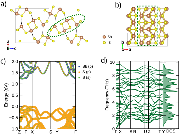
The orthorhombic phase of Sb2S3 belongs to the space group Pbnm with atoms per unit cell. Its crystal structure is highly anisotropic with covalently bonded 1D ribbons of Sb4S6 along the or direction (Figure 1(a)(b)). These ribbons are in turn weakly bonded in a zigzag fashion in the plane by van der Waals interactions. Due to the presence of van der Waals interactions, we test the nonlocal vdW-DF functional optB86b and SCAN+rVV10[26, 27] against some commonly used semi-local, metaGGA, and hybrid functionals[28, 29, 30, 31] (details in the Methods section). While most functionals are able to reproduce the lattice parameter accurately, the vdW functional performs the best at simultaneously reproducing and accurately due to its better performance at capturing the van der Waals interactions in the plane (see Table 1). There are little differences in the calculated lattice parameter between optB86b and SCAN+rVV10 functionals.
We then compute the orbital-projected band structure which is plotted in Figure 1(c). The valence band maximum (VBM) consists of mainly S orbitals and the conduction band minimum (CBM) is dominated by Sb-S bonds made up of Sb and S orbitals. The position of the VBM and CBM are located slightly away from at and , respectively. This means that Sb2S3 is an indirect bandgap semiconductor, which has been reported by previous theoretical studies[22], and experimentally observed in low temperature optical measurements by Fujita and co-workers [32].
The vdW functional suffers from the same self-interaction error as other semi-local and metaGGA functionals and underestimates the band gap to be around eV(Table 1). Using the hybrid functional HSE06 leads to a direct band gap of eV that is close to the experimental value. Our results are in general agreement with previously calculated band gaps in the range - eV at different levels of theory[22, 21, 20]. Due to the small difference between direct and indirect band gaps, meV, Sb2S3 is often treated as an effective direct band gap semiconductor. While hybrid functionals can more accurately reproduce the band gap, the computational cost is significantly larger than that of metaGGA functional like SCAN+rVV10, which in turns has higher computational cost than optB86b. We therefore use the optB86b functional for the electron-phonon calculations in this study and apply a HSE06-derived scissor shift to the band gaps when necessary. The computed phonon dispersion and density of states (DOS) is shown in Figure 1(d), which exhibits no imaginary modes[23] indicating dynamical stability.
For polaron calculations, hybrid functionals are necessary to describe the charge localization [33, 34, 35]. To determine the fraction of Fock exchange needed to cancel the self-interaction error, we verify the fulfillment of the Koopmans’ condition of the screened hybrid functional. This is done by calculating the occupied and unoccupied single particle energy levels related to the transition of an unrelaxed sulphur vacancy, which lies within the semiconductor gap of Sb2S3[36]. We vary the amount of exact Fock exchange while keeping the screening parameter constant at . Figure S1 shows the computed band edges and the energy levels for the sulphur vacancy transitions. We note that the single-particle energy levels shown in the figure include finite-size corrections[37, 38]. The crossing between the levels calculated in the and charge of the supercell corresponds to the value of exact exchange for which the Koopmans’ condition is satisfied. As this crossing value of is very close to the default value of in HSE06, we use the default Fock exchange for the subsequent polaron calculations.
.2 Temperature dependent structural and optical properties
| Material | (meV) | References |
|---|---|---|
| Sb2S3 | 200 | This study |
| Bi2S3 | 159 | [40] |
| GaAs | 96 | [41] |
| GaSb | 85 | [41] |
| MoS2 | 95 | [42] |
| WSe2 | 66 | [43] |
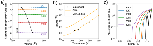
The first effect we consider for the description of the finite temperature optoelectronic properties of Sb2S3 is the role of thermal expansion. Using the quasi-harmonic approximation (QHA)[44], we consider primitive cell volumes ranging from Å3 to about Å3 in equidistant steps. As the unit cell of Sb2S3 is orthorhombic, the lattice parameters and atomic positions at each volumetric step are relaxed while keeping the volume constant. Then the Helmholtz free energies of the relaxed structures are calculated within the harmonic approximation to the lattice dynamics. Figure 2(a) depicts the Helmholtz free energy relative to the static lattice energy as a function of lattice volume for temperatures ranging from to K. The minimum of each fitted free-energy curve gives the quasi-harmonic volume at the corresponding temperature. The zero-point quantum motion contributes a volume increase of about Å3, and thermal expansion increases the volume by an additional Å3 in the studied temperature range.
Figure 2(b) shows the comparison between the experimental temperature dependent volume [39] and the QHA results. The raw DFT calculations overestimate the volume by a constant Å3 from K to K where experimental data are available, which is mainly due to the accuracy limits of the optB86b functional. There is remarkable agreement between theory and experiment if this systematic error is corrected, revealing that thermal expansion is correctly captured by our model.
Both and change by about meV when considering the influence of thermal expansion from K to K. This change is negligible compared to the absorption edge renormalization induced by electron-phonon coupling to be discussed next. Therefore, we will ignore the effects of thermal expansion in the rest of this work.
Figure 2(c) shows the absorption spectrum of Sb2S3 in logarithmic scale calculated with the optB86b functional and a HSE06-derived scissor correction. The static absorption spectrum shows sharp features due to the relatively small smearing parameter of meV used, which is nonetheless necessary to accurately locate the absorption onset. As the temperature increases, the optical absorption spectra are smoothed out by the continuous spectrum of allowed electronic states whose energies are renormalized by the inclusion of electron-phonon coupling effects (see Methods section for details). The absorption onset at K is about meV below that of the static level, indicating the importance of zero-point motion. Increasing temperature leads to a further red-shift of the absorption onset, a result that is consistent with recent experimental measurements of Bi2S3 in the chalcogenide family[40]. The calculated absorption onset changes by around meV from K to K, somewhat larger than that of meV reported for Bi2S3, but the difference likely arises from the mass difference between Bi and Sb[45]. Absorption onset redshifts of about meV have been observed in other conventional III-V or van der Waals semiconductors (see Table 2).
The large redshift in the temperature dependent absorption onset shows that Sb2S3 exhibits large electron-phonon coupling. Such strong coupling between electrons and phonons provides the necessary conditions for the possible generation of small localized polarons and STE which we discuss next.
.3 Carrier trapping
Spectroscopic studies on Sb2S3 show that the populations of the trapped carriers do not exhibit any saturation at high carrier density of cm-3, which suggests that the trapping is not due to defects as their concentrations are small[16, 18]. The polarized PL emission arising from the preferred dipole alignment of the trapped carriers also rule out the role of defects which are typically randomly distributed. These observations support that carriers in antimony dichalcogenides are self-trapped. However, the nature of the carrier trapping is unsolved as a first-principles study found that polarons in these systems exhibit large radii extending over several unit cells with moderate Fröhlich coupling constants[19]. Small polarons and therefore carrier self-trapping are unlikely to occur.
To resolve some of these controversies, we perform a systematic investigation of the polarons and bipolarons using a large supercell with 480 atoms. To find the polaronic geometry, we apply the bond distortion method to various bonds to break the symmetry of the crystal structure[46], which has shown to give faster convergence by mimicking the experimentally observed polaronic distortions. One excess electron is then added/removed from the supercell and the atomic positions are relaxed (see details in Methods section). We find that there is little resultant structural distortion, with little changes in the wavefunctions of the CBM and VBM states as shown in Figure S2. The excess electron is delocalized over the Sb atoms located on the edges of a [Sb4S6] ribbon, while the excess hole is delocalized over the entire supercell. Due to the delocalized nature of the band edge wavefunction, the formation energy of the excess carrier is calculated as the difference between the total energy of the supercell before and after structural relaxation. The formation energy of 4 meV is within the error of the DFT method and well below the energy of thermal fluctuations at room temperature, meaning that the formation of a small polaron is unlikely. These results are in agreement with the conclusions reached in the work of Wang et. al. [19].
We next investigate the addition/removal of two excess electrons, and note that the resultant excited carrier density of cm-3 is of the same order of magnitude as the carrier densities used in the transient absorption spectroscopy measurements of Sb2S3[16]. This motivates us to further explore the possible formation of bipolarons, which have been investigated in conjugated polymers and oxides for their roles on magnetoresistance and transport properties [47, 48, 49].
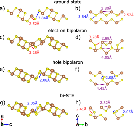
Similar to the search for polaronic structure, two excess electrons are added/removed from the supercell and the atomic positions relaxed after applying the bond distortion method. Compared with the ground state geometry (Figure 3(a,b)), there is a significant structural distortion with the elongation of the typical Sb-S bond from to Å with two excess electrons (Figure 3(c)). Within the [Sb4S6] chain, antimony dimers form with the nearest Sb-Sb distance decreasing from from to Å , while the S-S distance increases from to Å (Figure 3(d)). Dimer formation in the presence of bipolarons has been observed in oxides such as TiO2, LiNbO3 and BiVO4 [50, 51, 52]. The dimer formation can be understood from energetics: if the energy gained from the formation of the bonding orbitals between the antimony atoms is larger than the Coulomb repulsion between the two excess electrons, the two electron polarons can bind with each other and induce the dimerization[51]. The electron bipolaron state appears at the top of the valence bands (Figure 4(a)), with its wavefunction localized between two [Sb4S6] chains near the antimony dimers (Figure 4(b)(c)).
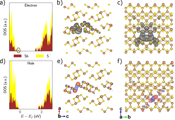
Analogously, the introduction of two excess holes results in the formation of a sulphur dimer between two neighbouring [Sb4S6] chains, with the S-S distance decreasing from to Å (Figure 3(e)(f)). The formation of the sulphur dimer pushes the state associated with its two holes far into the conduction band, where hybridization with conduction states occurs[51, 52]. For this reason, it is impossible to isolate these two holes for visualization. For illustrative purposes, we plot the difference between the total charge density of the hole bipolaron and the pristine Sb2S3 in Figure 4(d-f), resulting in the bonding orbitals between two sulphur atoms in the dimer. By modifying the defect formation energy expression, we compute the formation energies per carrier for electron and hole bipolarons as meV and meV (Equation 3).
We then construct a bi-STE from neighbouring electron and hole bipolarons by superimposing their structural distortions within a neutral simulation cell. The ground state electronic configurations are used and the system relaxes to a meta-stable configuration containing both the electron and hole bipolaron. As shown in Figure 3(g)(h), both the antimony and sulphur dimers still exist in this bi-STE structure, with their respective bond lengths further reduced compared to the individual bipolaron case. We note that a full description of excitons requires higher levels of theory than hybrid functionals, but a previous Bethe-Salpeter equation study of Sb2S3 indicates small exciton binding energies of meV[53]. The formation energy of the bi-STE per exciton is calculated as meV (Equation 4) and larger than the sum of the individual bipolaron, showing that these localized bipolarons further attract each other due to Coulomb interactions. The formation energy of the bi-STE is in general agreement with the reported Stokes shift of meV in Sb2S3. The slight overestimation from the calculation might arise from the accuracy of the band gap value of HSE06 hybrid functionals, as well as the structural deviation from the true excited state geometry of the bi-STE state.
Conclusion
We study electron-phonon coupling in the quasi-1D semiconductor Sb2S3. We first show that the optB86b nonlocal vdw-DF functional is the best choice for reproducing the experimental lattice parameters at reasonable computational cost. The quasi-harmonic approximation is capable of reproducing the thermal expansion coefficient and volumes agree well with experiments. We also find that the absorption edge red shifts by about meV from K to K, a higher value than the corresponding shift observed in most conventional and van der Waals semiconductors. This shows that there is significant electron-phonon coupling in the system. We further investigate the possibility of polaron, bipolaron, and bi-self-trapped-exciton (bi-STE) in the system. In the presence of one excess carrier, we find that no small polarons are formed in agreement with previous studies. With two excess carriers per supercell, electron and hole bipolarons can cause the formation of the sulphur and antimony dimers with relatively localized wavefunctions. The carrier densities of the bipolaron and bi-STE of cm-3 in our calculations agree well with experimental values in transient absorption experiments, and the bi-STE formation energy also agrees well with the experimentally measured Stokes shift. Our results reconcile some of the conflicting reports on carrier trapping in Sb2S3, and show that intrinsic self trapping can occur without the presence of defect states. Overall, large electron-phonon coupling and the presence of carrier self-trapping play an important role for the optoelectronic properties of Sb2S3, and might place a fundamental limit on the open circuit voltage of photovoltaic devices and consequently on the maximum efficiency of derived solar cells.
Methods
All DFT calculations are performed using the Vienna Ab initio Simulation Package (VASP, v5.4)[54, 55]. The core-valence interaction is described using the projector-augmented wave (PAW) method[56], with 5 valence electrons for Sb () and 6 valence electrons for S (). The electronic wave functions are expanded in a plane wave basis with an energy cutoff of eV, the Brillouin zone is sampled with a -centered Monkhorst-Pack[57] -point grid, and commensurate grids for the supercells. The atoms are relaxed until the Hellman-Feynman force converges below eVÅ-1, and the volume until all components of the stress tensor are below GPa.
All phonon dispersions are computed using the finite displacement method with a supercell containing atoms ( Å Å Å) as implemented in the Phonopy package[58]. For phonon dispersions, a non-analytical term is added to the dynamical matrix to treat the long range interaction arising from the macroscopic electric field induced by the polarization of collective ionic motions near [59].
To include the effects of electron-phonon interactions to optical absorption at a given temperature , we evaluate the imaginary part of the frequency-dependent dielectric function within the independent particle approximation using the Williams-Lax theory:
| (1) |
where is the vibrational wave function in state and with energy , evaluated within the harmonic approximation, and is the partition function in which is Boltzmann’s constant. For these calculations, we re-compute the phonon frequencies and eigenvectors using non-diagonal supercells[60], and then use them as a starting point to evaluate Equation (1) with Monte Carlo integration accelerated by thermal lines[61, 62].
From the finite temperature dielectric function, the absorption coefficient is given by , where is the speed of light in vacuum, is the imaginary part of the dielectric function, and is the real part of the complex refractive index. , and where is the real part of the dielectric function. is obtained from through the Kramers-Kronig relation. Convergence tests show that a supercell and a electronic -grid lead to accurate results.
For the fulfillment of the Koopmans’ condition, the corrections to the unoccupied Kohn-Sham eigenvalues of the defect-induced single particle levels are calculated as[63]
| (2) |
where is the charge of the defect, and is the finite size electrostatic correction. is computed using sxdefectalign[37] with an anisotropic screening where the diagonal terms of the high-frequency dielectric tensor are , , [64].
For polaron and self-trapped exciton (STE) calculations, we use a supercell to minimize spurious interactions between periodic images, and sample only the -point. After the addition or removal of an electron from the supercell, structural relaxation is performed using spin-polarized calculations whereby the supercell lattice parameters are fixed and the atoms allowed to move, with the same force convergence criterion of eVÅ-1. The binding energy of the electron or hole bipolaron per electron () can be estimated using the following formula for defect formation energy calculations[65]:
| (3) |
where is the total energy of the distorted supercell of the bipolaronic state, [pristine] is the total energy for the perfect crystal using an equivalent supercell, with denoting the excess of charge of an electron or hole, and is the energetic position of the CBM or VBM. The diagonal components of the static dielectric tensor are used with , , [64].
The formation energy of the bi-STE per exciton () is calculated as
| (4) |
where is the total energy of the distorted supercell of the bi-STE state with the ground state electronic configuration.
Acknowledgements
Y.L acknowledges funding support from the Simons Foundation (Grant 601946) and A*STAR under its Young Achiever Award. J.W. acknowledges funding from the Swedish Research Council (2019-03993). B.M. acknowledges support from a UKRI Future Leaders Fellowship (Grant No. MR/V023926/1), from the Gianna Angelopoulos Programme for Science, Technology, and Innovation, and from the Winton Programme for the Physics of Sustainability. This work was performed using resources provided by the Cambridge Service for Data Driven Discovery (CSD3) operated by the University of Cambridge Research Computing Service (www.csd3.cam.ac.uk), provided by Dell EMC and Intel using Tier-2 funding from the Engineering and Physical Sciences Research Council (capital grant EP/T022159/1), and DiRAC funding from the Science and Technology Facilities Council (www.dirac.ac.uk). We are also grateful for computational support from the UK national high performance computing service, ARCHER, for which access was obtained via the UKCP consortium and funded by EPSRC grant EP/P022561/1. We also acknowledge computational resources provided by the Swedish National Infrastructure for Computing (SNIC) at C3SE and PDC.
References
- Saga [2010] T. Saga, Advances in crystalline silicon solar cell technology for industrial mass production, NPG Asia Materials 2, 96 (2010).
- Jean et al. [2015] J. Jean, P. R. Brown, R. L. Jaffe, T. Buonassisi, and V. Bulovic, Pathways for solar photovoltaics, Energy and Environmental Science 8, 1200 (2015).
- Ehrler et al. [2020] B. Ehrler, E. Alarcón-Lladó, S. W. Tabernig, T. Veeken, E. C. Garnett, and A. Polman, Photovoltaics reaching for the shockley-queisser limit, ACS Energy Letters 5, 3029 (2020).
- Li and Zhang [2020] H. Li and W. Zhang, Perovskite tandem solar cells: From fundamentals to commercial deployment, Chemical Reviews 120, 9835 (2020).
- Kim et al. [2014] D.-H. Kim, S.-J. Lee, M. S. Park, J.-K. Kang, J. H. Heo, S. H. Im, and S.-J. Sung, Highly reproducible planar Sb S -sensitized solar cells based on atomic layer deposition, Nanoscale 6, 14549 (2014).
- Wang et al. [2017] L. Wang, D.-B. Li, K. Li, C. Chen, H.-X. Deng, L. Gao, Y. Zhao, F. Jiang, L. Li, F. Huang, Y. He, H. Song, G. Niu, and J. Tang, Stable 6%-efficient Sb2Se3 solar cells with a ZnO buffer layer, Nat Energy 2, 17046 (2017).
- Wang et al. [2018] X. Wang, R. Tang, C. Wu, C. Zhu, and T. Chen, Development of antimony sulfide–selenide sb2(s, se)3-based solar cells, Journal of Energy Chemistry 27, 713 (2018).
- Kondrotas et al. [2018] R. Kondrotas, C. Chen, and J. Tang, Sb2S3 Solar Cells, Joule 2, 857 (2018).
- Choi et al. [2014] Y. C. Choi, D. U. Lee, J. H. Noh, E. K. Kim, and S. I. Seok, Highly Improved Sb S Sensitized-Inorganic-Organic Heterojunction Solar Cells and Quantification of Traps by Deep-Level Transient Spectroscopy, Adv. Funct. Mater. 24, 3587 (2014).
- Ross Rucker et al. [2022] W. Ross Rucker, E. G. Sukenik, S. G. Rizzie, and D. P. Birnie, Thin film absorber selection to pair with silicon for 1-sun tandem photovoltaics, Solar Energy 238, 178 (2022).
- Darga et al. [2013] A. Darga, D. Mencaraglia, C. Longeaud, T. J. Savenije, B. O’Regan, S. Bourdais, T. Muto, B. Delatouche, and G. Dennler, On charge carrier recombination in sb2s3 and its implication for the performance of solar cells, The Journal of Physical Chemistry C 117, 20525 (2013).
- Cai and Chen [2020] Z. Cai and S. Chen, Extrinsic dopants in quasi-one-dimensional photovoltaic semiconductor Sb2S3: A first-principles study, Journal of Applied Physics 127, 183101 (2020).
- Maiti et al. [2020] A. Maiti, S. Chatterjee, and A. J. Pal, Sulfur-Vacancy Passivation in Solution-Processed Sb2S3 Thin Films: Influence on Photovoltaic Interfaces, ACS Applied Energy Materials 3, 810 (2020).
- Lian et al. [2021] W. Lian, C. Jiang, Y. Yin, R. Tang, G. Li, L. Zhang, B. Che, and T. Chen, Revealing composition and structure dependent deep-level defect in antimony trisulfide photovoltaics, Nature Communications 12, 3260 (2021).
- Wang et al. [2023] X. Wang, S. R. Kavanagh, D. O. Scanlon, and A. Walsh, Four-electron negative-u vacancy defects in antimony selenide (2023), arXiv:2302.04901 [cond-mat.mtrl-sci] .
- Yang et al. [2019] Z. Yang, X. Wang, Y. Chen, Z. Zheng, Z. Chen, W. Xu, W. Liu, Y. M. Yang, J. Zhao, T. Chen, and H. Zhu, Ultrafast self-trapping of photoexcited carriers sets the upper limit on antimony trisulfide photovoltaic devices, Nature Communications 10, 4540 (2019).
- Martin et al. [1997] P. Martin, S. Guizard, P. Daguzan, G. Petite, P. D’Oliveira, P. Meynadier, and M. Perdrix, Subpicosecond study of carrier trapping dynamics in wide-band-gap crystals, Phys. Rev. B 55, 5799 (1997).
- Tao et al. [2022] W. Tao, L. Zhu, K. Li, C. Chen, Y. Chen, Y. Li, X. Li, J. Tang, H. Shang, and H. Zhu, Coupled electronic and anharmonic structural dynamics for carrier self-trapping in photovoltaic antimony chalcogenides, Advanced Science 9, 2202154 (2022).
- Wang et al. [2022a] X. Wang, A. M. Ganose, S. R. Kavanagh, and A. Walsh, Band versus polaron: Charge transport in antimony chalcogenides, ACS Energy Letters 7, 2954 (2022a).
- Caracas and Gonze [2005] R. Caracas and X. Gonze, First-principles study of the electronic properties of a2b3 minerals, with a=bi,sb and b=s,se, Phys Chem Minerals 32, 295 (2005).
- Ben Nasr et al. [2011] T. Ben Nasr, H. Maghraoui-Meherzi, H. Ben Abdallah, and R. Bennaceur, Electronic structure and optical properties of sb2s3 crystal, Physica B: Condensed Matter 406, 287 (2011).
- Filip et al. [2013] M. R. Filip, C. E. Patrick, and F. Giustino, Gw quasiparticle band structures of stibnite, antimonselite, bismuthinite, and guanajuatite, Physical Review B - Condensed Matter and Materials Physics 87, 205125 (2013).
- Liu et al. [2014] Y. Liu, K. T. Eddie Chua, T. C. Sum, and C. K. Gan, First-principles study of the lattice dynamics of sb2s3, Phys. Chem. Chem. Phys. 16, 345 (2014).
- Gan et al. [2015] C. K. Gan, J. R. Soh, and Y. Liu, Large anharmonic effect and thermal expansion anisotropy of metal chalcogenides: The case of antimony sulfide, Physical Review B - Condensed Matter and Materials Physics 92, 235202 (2015).
- Bayliss and Nowacki [1972] P. Bayliss and W. Nowacki, Refinement of the crystal structure of stibnite, sb2s31, Zeitschrift für Kristallographie 135, 308 (1972).
- Klimeš et al. [2011] J. Klimeš, D. R. Bowler, and A. Michaelides, Van der Waals density functionals applied to solids, Phys. Rev. B 83, 195131 (2011).
- Peng et al. [2016] H. Peng, Z.-H. Yang, J. P. Perdew, and J. Sun, Versatile van der Waals Density Functional Based on a Meta-Generalized Gradient Approximation, Phys. Rev. X 6, 041005 (2016).
- Perdew et al. [1996] J. P. Perdew, K. Burke, and M. Ernzerhof, Generalized gradient approximation made simple, Physical Review Letters 77, 3865 (1996).
- Sun et al. [2016] J. Sun, R. C. Remsing, Y. Zhang, Z. Sun, A. Ruzsinszky, H. Peng, Z. Yang, A. Paul, U. Waghmare, X. Wu, M. L. Klein, and J. P. Perdew, Accurate first-principles structures and energies of diversely bonded systems from an efficient density functional, Nature Chem 8, 831 (2016).
- Perdew et al. [2008] J. P. Perdew, A. Ruzsinszky, G. I. Csonka, O. A. Vydrov, G. E. Scuseria, L. A. Constantin, X. Zhou, and K. Burke, Restoring the Density-Gradient Expansion for Exchange in Solids and Surfaces, Phys. Rev. Lett. 100, 136406 (2008).
- Heyd et al. [2003] J. Heyd, G. E. Scuseria, and M. Ernzerhof, Hybrid functionals based on a screened Coulomb potential, The Journal of Chemical Physics 118, 8207 (2003).
- Fujita et al. [1987] T. Fujita, K. Kurita, K. Takiyama, and T. Oda, The fundamental absorption edge and electronic structure in sb2s3, Journal of the Physical Society of Japan 56, 3734 (1987).
- Ouhbi and Wiktor [2021] H. Ouhbi and J. Wiktor, Polaron formation and hopping in tantalate perovskite oxides: NaTaO 3 and KTaO 3, Phys. Rev. B 104, 235158 (2021).
- Janotti et al. [2014] A. Janotti, J. B. Varley, M. Choi, and C. G. Van de Walle, Vacancies and small polarons in SrTiO 3, Phys. Rev. B 90, 085202 (2014).
- Spreafico and VandeVondele [2014] C. Spreafico and J. VandeVondele, The nature of excess electrons in anatase and rutile from hybrid DFT and RPA, Phys. Chem. Chem. Phys. 16, 26144 (2014).
- Cai et al. [2020] Z. Cai, C.-M. Dai, and S. Chen, Intrinsic defect limit to the electrical conductivity and a two-step p-type doping strategy for overcoming the efficiency bottleneck of sb2s3-based solar cells, Solar RRL 4, 1900503 (2020).
- Freysoldt et al. [2009] C. Freysoldt, J. Neugebauer, and C. G. Van de Walle, Fully ab initio finite-size corrections for charged-defect supercell calculations, Phys. Rev. Lett. 102, 016402 (2009).
- Falletta et al. [2020] S. Falletta, J. Wiktor, and A. Pasquarello, Finite-size corrections of defect energy levels involving ionic polarization, Physical Review B 102, 041115 (2020).
- Kyono et al. [2002] A. Kyono, M. Kimata, M. Matsuhisa, Y. Miyashita, and K. Okamoto, Low-temperature crystal structures of stibnite implying orbital overlap of Sb 5s2 inert pair electrons, Physics and Chemistry of Minerals 29, 254 (2002).
- Linhart et al. [2021] W. M. Linhart, S. J. Zelewski, P. Scharoch, F. Dybała, and R. Kudrawiec, Nesting-like band gap in bismuth sulfide Bi S , J. Mater. Chem. C , 10.1039.D1TC03625D (2021).
- Vurgaftman et al. [2001] I. Vurgaftman, J. R. Meyer, and L. R. Ram-Mohan, Band parameters for iii–v compound semiconductors and their alloys, Journal of Applied Physics 89, 5815 (2001).
- Sigiro et al. [2015] M. Sigiro, Y.-S. Huang, C.-H. Ho, Y.-C. Lin, and K. Suenaga, Influence of rhenium on the structural and optical properties of molybdenum disulfide, Japanese Journal of Applied Physics 54, 04DH05 (2015).
- Arora et al. [2015] A. Arora, M. Koperski, K. Nogajewski, J. Marcus, C. Faugeras, and M. Potemski, Excitonic resonances in thin films of wse2: from monolayer to bulk material, Nanoscale 7, 10421 (2015).
- Togo et al. [2010] A. Togo, L. Chaput, I. Tanaka, and G. Hug, First-principles phonon calculations of thermal expansion in Ti 3 SiC 2 , Ti 3 AlC 2 , and Ti 3 GeC 2, Phys. Rev. B 81, 174301 (2010).
- Shang et al. [2021] H. Shang, J. Zhao, and J. Yang, Assessment of the mass factor for the electron–phonon coupling in solids, The Journal of Physical Chemistry C 125, 6479 (2021).
- Pham and Deskins [2020] T. D. Pham and N. A. Deskins, Efficient Method for Modeling Polarons Using Electronic Structure Methods, Journal of Chemical Theory and Computation 16, 5264 (2020).
- Cohen et al. [1984] M. H. Cohen, E. N. Economou, and C. M. Soukoulis, Small-bipolaron formation, Phys. Rev. B 29, 4496 (1984).
- Wagemans et al. [2008] W. Wagemans, F. L. Bloom, P. A. Bobbert, M. Wohlgenannt, and B. Koopmans, A two-site bipolaron model for organic magnetoresistance, Journal of Applied Physics 103, 07F303 (2008).
- Devreese and Alexandrov [2009] J. T. Devreese and A. S. Alexandrov, Fröhlich polaron and bipolaron: recent developments, Rep. Prog. Phys. 72, 066501 (2009).
- Schirmer et al. [2009] O. F. Schirmer, M. Imlau, C. Merschjann, and B. Schoke, Electron small polarons and bipolarons in LiNbO , J. Phys.: Condens. Matter 21, 123201 (2009).
- Chen and Wang [2014] S. Chen and L.-W. Wang, Double-hole-induced oxygen dimerization in transition metal oxides, Phys. Rev. B 89, 014109 (2014).
- Österbacka et al. [2022] N. Österbacka, F. Ambrosio, and J. Wiktor, Charge Localization in Defective BiVO , J. Phys. Chem. C 126, 2960 (2022).
- Caruso et al. [2015] F. Caruso, M. R. Filip, and F. Giustino, Excitons in one-dimensional van der Waals materials: Sb2 S3 nanoribbons, Physical Review B - Condensed Matter and Materials Physics 92, 10.1103/PhysRevB.92.125134 (2015).
- Kresse and Furthmüller [1996a] G. Kresse and J. Furthmüller, Efficient iterative schemes for ab initio total-energy calculations using a plane-wave basis set, Physical Review B - Condensed Matter and Materials Physics 54, 11169 (1996a).
- Kresse and Furthmüller [1996b] G. Kresse and J. Furthmüller, Efficiency of ab-initio total energy calculations for metals and semiconductors using a plane-wave basis set, Computational Materials Science 6, 15 (1996b).
- Blöchl [1994] P. E. Blöchl, Projector augmented-wave method, Phys. Rev. B 50, 17953 (1994).
- Monkhorst and Pack [1976] H. J. Monkhorst and J. D. Pack, Special points for Brillouin-zone integrations, Physical Review B 13, 5188 (1976).
- Togo [2015] A. Togo, First principles phonon calculations in materials science, Scripta Materialia , 5 (2015).
- Gonze and Lee [1997] X. Gonze and C. Lee, Dynamical matrices, Born effective charges, dielectric permittivity tensors, and interatomic force constants from density-functional perturbation theory, Phys. Rev. B 55, 10355 (1997).
- Lloyd-Williams and Monserrat [2015] J. H. Lloyd-Williams and B. Monserrat, Lattice dynamics and electron-phonon coupling calculations using nondiagonal supercells, Phys. Rev. B 92, 184301 (2015).
- Monserrat [2016] B. Monserrat, Vibrational averages along thermal lines, Physical Review B 93, 014302 (2016).
- Monserrat [2018] B. Monserrat, Electron-phonon coupling from finite differences, Journal of Physics Condensed Matter 30, 083001 (2018).
- Chen and Pasquarello [2013] W. Chen and A. Pasquarello, Correspondence of defect energy levels in hybrid density functional theory and many-body perturbation theory, Physical Review B 88, 115104 (2013).
- Wang et al. [2022b] X. Wang, Z. Li, S. R. Kavanagh, A. M. Ganose, and A. Walsh, Lone pair driven anisotropy in antimony chalcogenide semiconductors, Phys. Chem. Chem. Phys. 24, 7195 (2022b).
- Freysoldt et al. [2014] C. Freysoldt, B. Grabowski, T. Hickel, J. Neugebauer, G. Kresse, A. Janotti, and C. G. Van De Walle, First-principles calculations for point defects in solids, Reviews of Modern Physics 86, 253 (2014).
- Momma and Izumi [2008] K. Momma and F. Izumi, VESTA : a three-dimensional visualization system for electronic and structural analysis, J Appl Crystallogr 41, 653 (2008).
- M Ganose et al. [2018] A. M Ganose, A. J Jackson, and D. O Scanlon, sumo: Command-line tools for plotting and analysis of periodic ab initio calculations, JOSS 3, 717 (2018).