Bayesian autotuning of Hubbard model quantum simulators
Abstract
Spins in gated semiconductor quantum dots (QDs) are a promising platform for Hubbard model simulation inaccessible to computation. Precise control of the tunnel couplings by tuning voltages on metallic gates is vital for a successful QD-based simulator. However, the number of tunable voltages and the complexity of the relationships between gate voltages and the parameters of the resulting Hubbard models quickly increase with the number of quantum dots. As a consequence, it is not known if and how a particular gate geometry yields a target Hubbard model. To solve this problem, we propose a hybrid machine-learning approach using a combination of support vector machines (SVMs) and Bayesian optimization (BO) to identify combinations of voltages that realize a desired Hubbard model. SVM constrains the space of voltages by rejecting voltage combinations producing potentials unsuitable for tight-binding (TB) approximation. The target voltage combinations are then identified by BO in the constrained subdomain. For large QD arrays, we propose a scalable efficient iterative procedure using our SVM-BO approach, which optimises voltage subsets and utilises a two-QD SVM model for large systems. Our results use experimental gate lithography images and accurate integrals calculated with linear combinations of harmonic orbitals to train the machine learning algorithms.
I Introduction
Recent progress in manipulating spins in gated semiconductor quantum dots (QDs) [1, 2, 3] offers an opportunity for realizing scalable quantum systems for applications in quantum computing [4, 5, 6, 7, 8, 9] and simulation, such as Kitaev chain or Hubbard model simulation [10, 11, 12, 13, 14]. Hubbard models with many sites, inhomogeneous or time-varying parameters remain largely unexplored due to computational complexity, but can be studied experimentally with new generations of gated QD arrays. A successful QD-based device appropriate for this goal must provide means to control the charge occupation, chemical potential of QDs and tunnel couplings with considerable precision in order to prepare, manipulate and read out many-particle quantum states [4, 15, 16, 5]. Therefore, developing the tools to identify the charge states and tune their properties to desired operating regimes is vital for scaling up the complexity of quantum simulators and discovering new physical phenomena, such as topological phases [17, 11, 18, 19, 20] and strongly-correlated ground states [16, 10, 12, 13, 14, 21]. In particular, the inter-dot tunneling amplitude requires special attention as it determines the exchange interaction of spins in QDs [22, 16], which affects all their applications, ranging from qubit design to parameters of interacting electron models under study.
Design of QD-based simulator relies on well-established techniques of trapping electrons in electrostatic potential wells, i.e. QDs, created at the interface of semiconductor devices build with silicon [23, 1, 2], germanium [24, 3], III-V materials [25, 26, 27, 13] or 2D semiconductors [28, 29, 30, 31, 32, 33, 7, 34]. This confining potential landscape is determined by a set of voltages applied to lithographically fabricated metallic gates placed on top of the nanomaterial. Contacts are reservoirs of electrons placed at the edges of the structure to allow for electron tunneling into the confining potential wells, where they can be manipulated. Barrier gates are used to control tunneling between QDs, while plunger gates are designed to alter the depth of each potential well. Changing the voltages on all those gates allows for realizing a vast range of electron states for various applications. Characterization of charge states achieved with different voltage combinations is usually performed by repeatedly measuring the charge stability diagram – an image of transport features as a function of gate voltages, essential for experimentally tuning the system to a desired regime [26, 35].
This approach to control the gate voltages limits the scalability of QD-based simulators. For systems with many quantum dots, the number of gates is large and the design complexity makes the voltage calibration process impractical for manual tuning. Moreover, in dense devices, the relative proximity of gates produces substantial cross-talk, which further complicates the independent QD control [36, 12, 37, 38]. An additional obstacle for practical QD simulators is the presence of charge impurities unavoidable in the fabrication process, which alter the potential landscape and lead to non-uniform device performance [36, 12, 37]. These challenges, combined with variations of gate geometry, and a wide range of material parameters and screening effects impede the development of practical tools for experimental control of QD-based simulators.
Machine learning (ML) has emerged as a promising tool for some of the experimental challenges with QD control [37]. Deep neural networks [39, 40, 41, 42, 43, 44, 45, 46], image recognition [47, 40, 48, 38, 42, 49, 50] and supervised classification [40, 51, 46] have been demonstrated to aid charge state characterization [41, 48, 51, 42, 49], coupling parameter tuning [37] and gate voltage optimization [36, 41, 52, 49, 43, 46] in a single QD [51, 49, 43], double QDs [36, 37, 38, 51, 42, 43, 44], triple QDs and arrays of QDs [36, 37, 41, 48, 45]. Unsupervised statistical methods [52, 53] and deterministic algorithms [36, 51, 49, 50] have also been used for double-QD tuning. ML also proven useful for compensating for cross-capacitance in devices [45], calibration of virtual gates in place of real ones [48, 45] and in the analysis and parameter-extraction from charge stability diagrams [48].
A vast majority of these approaches relied on experimentally obtained data as input [48, 38] or intermediate step in a feedback protocol [36, 37, 51, 42, 49, 52], which required numerous measurements or involved readjustments and recapturing procedures [36, 37, 51, 42, 49, 43, 53, 52]. Although scarcity of experimental data has been addressed in Refs [43, 44] with synthetic data, many ML solutions for QD simulators suffer from crude theoretical assumptions. This includes the Thomas-Fermi approximation for electron density [54, 44], the use of exponential fits to tunneling couplings [48] or constant interaction model with weak coupling and absent barrier gates [50], which limits their applicability to a wider range of designs and materials. Another limitation of the optimization techniques used in Refs [38, 45] is the need for obtaining the gradients of gate voltages in the parameter search, which may be prone to vanishing gradient problem [55]. The relationship between gate voltages and the parameters of the resulting quantum simulator is further complicated by the scarcity of the physical simulation domain: the majority of the voltage combinations produce unphysical potentials. Thus, an automated first-principle design of quantum simulators must be able to recognize the physical subdomain of experimentally tunable parameters.
To address this problem, we propose a hybrid machine-learning approach using a combination of support vector machines (SVMs) and Bayesian optimization to identify combinations of voltages that realize a desired Hubbard model. SVM constrains the space of voltages by rejecting voltage combinations producing potentials unsuitable for tight-binding (TB) approximation. The target voltage combinations are then identified by Bayesian optimization (BO) in the constrained subdomain. We perform BO of gate voltages to produce a double QD system with tailored tunneling parameter and on-site Hubbard energy , using experimental gate lithography images as input for realistic calculations of and with the linear combination of harmonic orbitals method (LCHO) [56]. This approach allows us to predict and for variable electrode design and with flexible material parameters and custom heterostructures. Our BO procedure operates without gradients or input from experimental charge stability diagrams, which are tedious to measure for large systems. BO is also suitable for problems with multiple local optima and noisy data. We also develop an iterative, scalable SVM-BO approach for multiple-site arrays, which is able to reach optimal solution by only optimising subsets of voltages at a time and uses only the two-site SVM. We predict the optimal voltage combination needed in experiment to prepare an on-demand double QD Hubbard model within 1.5% error for model gates and 6% for experimental gates, as well as for three-site system with error. This procedure can be combined with existing methods of preparing a charged state within quantum dots [36, 41, 48, 51, 42, 49, 52, 43, 46].
This paper is organized as follows: Section I describes the numerical calculations of the electrostatic potentials from the metallic gate input image by solving Poisson’s equation. Section II presents the SVM model developed to classify voltage combinations and demonstrates its excellent performance for rejecting undesired voltage combinations for two gate designs: an ideal simple-shaped gate set and a realistic experimental gate set obtained from lithography images. Section III describes the LCHO method for the calculation of the Hubbard model parameters and presents the results for possible ratios that can be achieved with various gate designs. The adaptation of BO for the title problem is described in Section IV. We present our results on optimal voltage combinations for the model and experimental sets of gates in Section V.
II Electrostatic potential from metallic gates
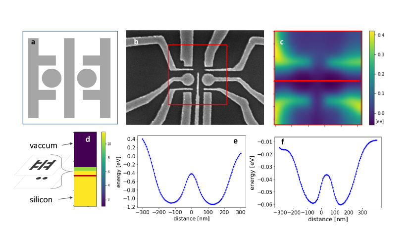
We begin by computing the electrostatic confining potential produced by two sets of metallic gates: the model basic-shape gates in Fig. 1 and a realistic gate image from experiment [57] in Fig. 1. Both sets of metallic gates are assumed to be 10 nm tall and are placed within a heterostructure inside a material with (Fig. 1). The pattern of the gates serves as input to a finite difference numerical method solving the Poisson’s equation:
| (1) |
where is the position vector in 3D space, is the charge density, is the dielectric constant and is the permittivity of free space.
We use finite difference method with the varied dielectric constant and two types of boundary conditions: the Dirichlet boundary condition at the top and bottom of computational box as well as inside the box, where the gate is placed, the Neumann boundary condition at the sides of the computational box, in and direction. We use a grid of 150150127 points in directions. The sample is modeled with of vaccum above the heterostructure and wetting layer below the metallic gate layer. The successive over-relaxation technique [58] is used to speed up the numerical procedure.
Fig 1 shows the resulting 2D electrostatic potential (for experimental gates) for an sample set of voltages, consisting of two confining wells (quantum dots) which act as sites in a 2-site Hubbard model. The red line marks a 1D cut of the potential passing through the minima of the two wells. The 1D example potential cuts for model as well as experimental gates are shown in Fig. 1.
III Hubbard model simulation domain
In a typical experiment with gated QDs, each QD is tuned by electrodes. As the number of QDs increases as needed for many-site Hubbard models, the space of gate voltages becomes high-dimensional. More importantly, the vast majority of the gate voltage combinations results in electrostatic potentials that are unsuitable for quantum simulation of Hubbard models and must, therefore, be discarded as unphysical. Identifying the target gate voltages thus amounts to optimization in a highly constrained subdomain.
In order to identify the subdomain of gate voltages producing suitable potentials, we develop an SVM filter of gate voltages. We use SVM to solve a classification problem as implemented in the scikit-learn python library [59] with a radial basis function (RBF) kernel. The SVM models are trained by the results of single-particle (SP) quantum calculation. For a given combination of voltages, we obtain the electrostatic potential as described in Section II and solve the Schrödiger equation to obtain the particle density for lowest-energy eigenstates.
We adopt the following criteria for the classification problem. The gate voltages are accepted as suitable for quantum simulation of the Hubbard models provided: a) a significant portion of the particle density in well 1 or 2 ( or ) is enclosed within a given radius from the centres of the quantum dots (and the charge density within any single well does not vanish); b) a chemical potential is set and all SP energy levels are populated, i.e. . For the present calculations, we use nm, eV. SVM is trained over training points and achieves approximately overall success and above rejection success.

The classification problem we consider here is imbalanced, i.e. around of the potentials are suitable for Hubbard model. In practice, it is important to tune this step to be sensitive to rejection in order not to perform further optimisation on unphysical potentials. Fig. 2 a) and b) show examples of potentials from model gates which have been correctly accepted and rejected respectively. The grey line represent all potentials included in classification. It is apparent that the accepted potentials all exhibit an acceptable shape for TB, while rejected onces have chaotic shapes. Fig 2 c) shows examples of incorrectly accepted potentials, which are still physical and can be confidently passed on to the next step. The results of Fig. 2 show that the filter can be reliably used to respect the TB assumption and produce two-site potentials suitable for Hubbard model simulation.
Fig 2 d) shows example cuts within the high-dimensional voltage space with the classification label given by the present SVM model (yellow/ purple is accepted/rejected), which illustrates the significant reduction of the search space.
For more than two QDs, the space of voltages becomes even more restrictive and building a reliable SVM model is challenging. We found that approx. and approx. of potentials were acceptable for three and four QDs, respectively. This is mainly because for more QDs, the first several SP energy shells should be aligned in order to allow tunnelling, and it is exponentially harder to achieve with growing number of voltages. However, the primary aim of the SVM model in our optimisation is to identify the physical potentials for Hubbard model parameter calculation. If this task is done correctly, the alignment of energy levels can be achieved by a simple check following the SVM classification. Due to this, we find that it is sufficient to use the SVM model for two QDs to classify subsets of voltages for more QDs, provided that the gate geometry does not change significantly with more QDs. Detailed explanation of how this is used in practice is given in Sec. V.
IV The Hubbard model parameters
We seek to design and optimize the quantum simulator of a Hubbard model, where the quantum dots act as sites for charges. The Hamiltonian of the Hubbard model with spin-degenerate orbitals per dot can be written as follows:
| (2) |
where and index orthogonal orbitals in individual sites, is the creation (annihilation) operator of a particle on site , orbital with spin and and are the parameters of the desired Hubbard model.
The Hubbard model parameters are uniquely determined by the confining potential created by the metallic gates and can be calculated for a given potential with the LCHO method [56]. In order to use LCHO, we consider the parts of the numerical potential that correspond to individual sites and solve the SP single-QD problem for each one of them. This serves as a basis for many-site LCHO calculation. In our optimisation procedure, the QD separation is varied approximately by translating the single-QD solution in space to calculate integrals at variable distances.
We now briefly describe the LCHO method. The dimensionless SP Hamiltonian in the two dimensional potential of a double QD reads:
| (3) |
where we express all distances in effective Bohr radii and all energies in units of the effective Rydberg and , and nm. In Eq. 3 are the potentials for a single quantum dot , which are well approximated by a 2D harmonic oscillator (HO) potential at the bottom of the well , where denotes the strength of the potential on dot , is the centre position of the quantum dot, is the characteristic width and represents deviation from the HO potential. This motivates the choice of the basis as the set of 2D HO eigenfunctions with corresponding eigenvalues . The 3D wavefunction of a particle is a product of the linear combination of HO orbitals on each dot
| (4) |
with the eigenfunction of the infinite narrow square quantum wall in direction , . Substituting Eq. 4 in the eigenvalue problem of Eq. 3 and multiplying by on the left we get
| (5) |
where denotes a composite index and indexes eigenstates of Eq. 3. Eq. 5 is the generalised eigenvalue problem for : , where is the overlap matrix with elements .
The parameters and of the Hubbard model Hamiltonian in Eq. 2 can be found as the matrix elements of the Hamiltonian matrix in the basis of orthogonal orbitals : .
The parameters from Eq. 2 can be obtained by evaluating the many-particle integrals in the orthogonal basis:
| (6) |
where is a 3D vector, is Coulomb interaction and . We perform these 6D integrals using the vegas phyton library [60, 61], which allows for Monte Carlo estimates of arbitrary multidimensional integrals.
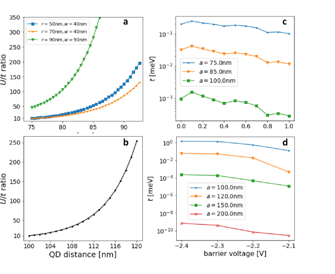
In Fig. 3 we show examples of resulting Hubbard integrals for a two-site system, where and . As expected, as the quantum dot distance decreases, the ratio drops (Fig 3 a). Wider barriers decrease hopping and increase the ratio, while bigger QD radii cause the dependence to grow at a smaller rate. Fig 3 b) shows the value of for a selected voltage combination with the middle barrier voltage variable, for several quantum dot distances. As the barrier grows, the hopping is reduced.
V Bayesian optimization of voltages
Here we present the algorithm we use to define the optimal set of gate voltages in order to realise a desired Hubbard model experimentally with a chain of electrostatically defined quantum dots. The Hubbard model is defined by the integrals given in Eq. 2, and, for constant QD radius - mainly by , which becomes the optimised quantity in our procedure, depicted in Fig. 5. We set a goal for the value of value and vary the voltages as well as the quantum dot distance iteratively until an optimal combination is found. Changing the set of voltages and distance modifies the potential landscape, which is evaluated by the SVM classifier for suitability for Hubbard model realisation. Only the accepted potentials are used in the integral calculation stage to yield . Finally, a new sample is selected and the classification and evaluation steps are repeated.
We use Bayesian optimisation (BO) [62, 63] to find the optimum voltage and distance combination , which produces integrals as close to the desired value as possible. We choose this method due to the black-box nature of the evaluated function and because no derivative calculation is needed. Also, as several combinations may produce a desired Hubbard model, BO is particularly suitable because of its suitability for non-convex problems.
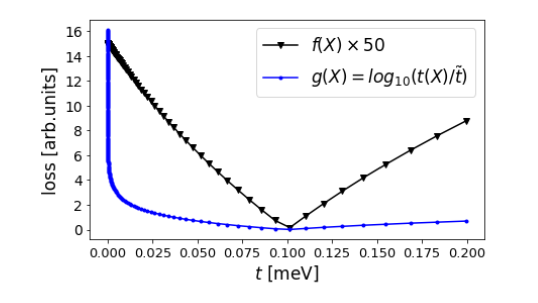
For the two-site problem, with a constant size of plunger gates, integrals are slowly varying and achieving a variety of values would require size adjustment. For a costant diameter of the quantum dots, we choose the loss function for BO dependent primarily on the value of hopping , which spans many orders of magnitude. Because of the variations in value of , the BO loss function must include the logarithm . However, as in most of the voltage space, these regions need to correspond to a slowly varying loss function, and fast loss variations should only be allowed close to the minimum to guide the acquisition of new points. Therefore we define the BO loss function as follows:
| (7) |
Function is shown in Fig. 4 in contrast to , which invovles large value changes in unimportant regions of . In Eq. 7, is a constant value assigned to a case when the potential is rejected by SVM and it is introduced in order to constrain the optimisation domain of . We choose , a value that reaches in extreme case if is very small. An optimal combination for achieving desired as well as is selected from these sampled points which optimise well for but correspond to best as well.
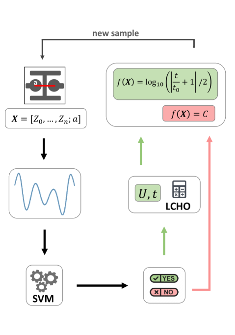
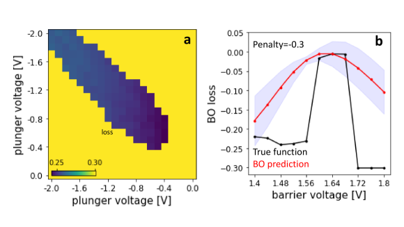
Fig. 6 a) shows the value of the loss function in Eq. 7 for a cut in the voltage space (darker blue corresponds to lower loss values). Fig. b) shows the prediction of the underlying GP after iterations for a single voltage path around a local optimum for . The true loss values (GP mean) are shown in black (red) and the GP variance is shown in shaded blue. GP follows the trend of the true loss function, and agrees with it around the local maximum. This allows for efficient selection of new points to sample using the acquisition function.
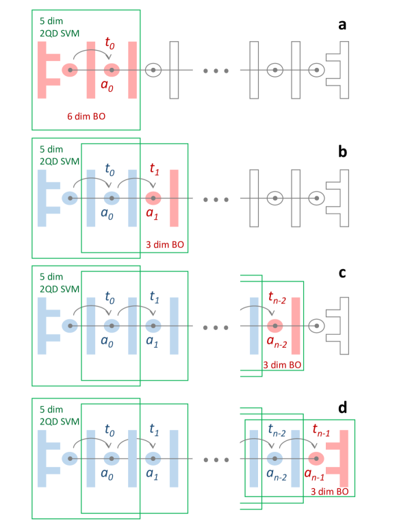
We now discuss the iterative approach to the voltage optimisation of linear arrays of more QDs, outlined in Fig. 7. We found that classifying subsets of voltages yields physical potentials, even for more than two QDs. We therefore use the unchanged SVM model built for two QD array to classify sets of five voltages a time, as shown with green boxes in Fig. 7. We begin with 6D BO optimisation of first five voltages (and lattice constant ), shown in red, and use the SVM model in each iteration for classification (Fig. 7 a), shown in green. The outcome is the optimal and the optimal parameters . In the next step, shown in Fig. 7 b), we freeze the parameters obtained in the previous step (shown in blue), and perform a 3D BO of the pair of neighbouring voltages and distance to the next QD (shown in red). In this step, we still use the unaltered SVM model to classify every voltage sample, made of three frozen (blue) voltages and two variable (red) voltages. As a result we obtain next set of optimal parameters and the optimal . We continue in this fashion (Fig. 7 c), until the full structure has been optimised (Fig 7 d).
The benefit of this iterative approach is that we are able to use BO for large systems without increasing the otpimisation problem dimension. Moreover, a single SVM model built for a small system can be used to optimise big structures. We also find that even for more QDs, a similar number of BO iterations is needed to achieve a satisfactory optimum. To ensure that all tunnelling integrals are within the range of the set goal we always pick the best optimum from a range of best solutions. This is because the neighbouring gates influence the previously optimised values, e.g. for three QDs, we found that the variation of during optimisation targeted for is approx. for all satisfactory . We expect that this effect is local and will only significantly affect the neighbouring QDs in a bigger structure. To remedy the variations of the previously optimised , we pick the best solution that achieves the goal for both values. This approach is straightforward in implementation, scalable to large systems and avoids the complexity of multi-targeted optimisation.
VI Results
Here we present the results of our optimisation of gate voltages with a chosen goal of meV for model gates and meV for experimental gates. We run BO for the 5 dimensional model gate voltage space with boundaries at eV and eV. We test several parameters for the function and choose the best results.
Fig. 8 a) and b) show the loss values as the optimisation progresses for model and experimental gate designs respectively. The target has been marked with red line and the best solutions have been marked with green dots. Only iterations with positive SVM label are shown. It is apparent for both cases that the algorithm quickly abandons the regions of negligible and zooms in around local minima, while values grow. Initially around of new acquired points are labeled as positive and this proportion grows to about .
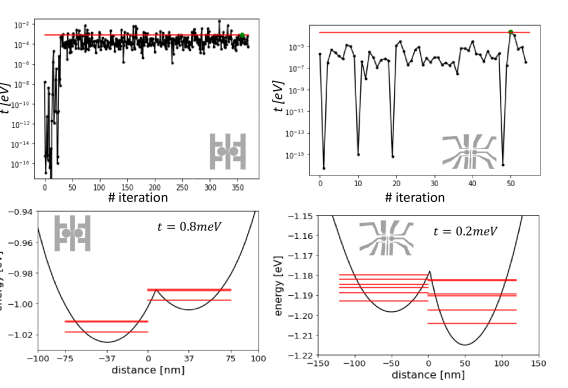
Fig. 8 c) and d) show the approximate potential for best found voltage and distance set produced by translation of single-QD potentials to optimal . The goal has been reached with error () for model (experimental) gates. Single-QD eigenenergies are shown in red in each quantum well. As no condition on QD bottom energy difference has been imposed, the bottom energies are meV apart in both cases. In order to achieve high hopping values , a small distance was needed. This calculation also served as a guide on possible values achievable for given designs. The resulting nm for experimental design is possible to reproduce in experiment with current fabrication technology [3, 57].
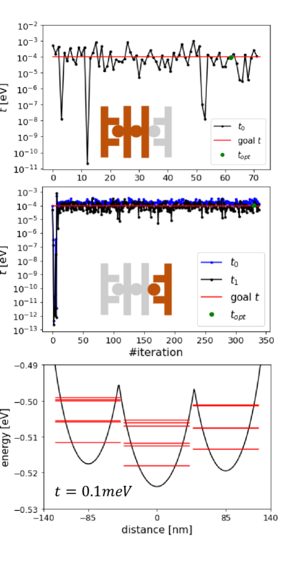
In Fig. 9 we present the results of the iterative BO approach for three QD array. Fig. 9 a) and b) show the evolution of the value of (black, goal shown in red) and (blue, black, goal shown in red) in steps and of the iterative procedure. Red gates are varied while grey remain frozen. Both steps included 1000 BO iterations, but due to higher dimensionality of step than step , fewer points in space are accepted by the SVM model, so the curve is more sparse. Fig. 9 b) shows that for satisfactory , variations of are much smaller than , which allows us to pick pairs of best meeting the goal.
Fig. 9 c) shows the best three QD potentials that achieves both goals of within error, while maintaining the alignment of the QD SP energy level ranges. The optimised distance for both steps and was found to be the same, up to less than .
VII Conclusions
We used machine learning techniques for the experimental voltage setup optimization that produces the target Hubbard and parameters and allows for tailored Hubbard model simulation. Using SVM we classified potential profiles based on suitability for tight-binding approximation reducing the space by 99%. We then optimized the voltage combinations using Bayesian optimization, which operates without evaluating gradients of the loss function or experimental stability diagram input. Our results rely on accurate experimental gate images and realistic integrals based on LCHO calculation. We were able to predict voltages needed in experiment to prepare on demand double QD Hubbard model within 1.5% error for model gates and 6% error for experimental gates.
We also designed an iterative procedure using several Bayesian optimisation instances, one for each extra QD above two QDs. It involves the optimisation of subsets of voltages, which allows for scaling to large systems, and targets a single tunnelling integral at a time, which avoids high complexity of multi-target approaches. Importantly, we use the same SVM model trained for two QDs to classify subsets of voltages in each iteration, so training exponentially hard SVM models can be avoided for bigger arrays. We reach an accuracy of 10% for both tunnelling parameters within the same number of iterations as used for two-QD system.
This procedure demonstrates how on-demand Hubbard models can be prepared in experiments to explore new Hubbard physics. It could be embedded in a larger algorithm to reliably tune tunnelling couplings with BO and prepare charge states using existing experiment-based methods.
VIII Acknowledgements
We thank E. Sajadi, M. Tanvir and J. Salfi for discussions and permission to use the experimental image in Fig. 1. b).
References
- Maune et al. [2012] B. M. Maune, M. G. Borselli, B. Huang, T. D. Ladd, P. W. Deelman, K. S. Holabird, A. A. Kiselev, I. Alvarado-Rodriguez, R. S. Ross, A. E. Schmitz, M. Sokolich, C. A. Watson, M. F. Gyure, and A. T. Hunter, Coherent singlet-triplet oscillations in a silicon-based double quantum dot, Nature 481, 344 (2012).
- Maurand et al. [2016] R. Maurand, X. Jehl, D. Kotekar-Patil, A. Corna, H. Bohuslavskyi, R. Laviéville, L. Hutin, S. Barraud, M. Vinet, M. Sanquer, and S. De Franceschi, A CMOS silicon spin qubit, Nature Communications 7, 13575 (2016).
- Hendrickx et al. [2021] N. W. Hendrickx, W. I. L. Lawrie, M. Russ, F. van Riggelen, S. L. de Snoo, R. N. Schouten, A. Sammak, G. Scappucci, and M. Veldhorst, A four-qubit germanium quantum processor, Nature 591, 580 (2021).
- Loss and DiVincenzo [1998] D. Loss and D. P. DiVincenzo, Quantum computation with quantum dots, Physical Review A 57, 120 (1998).
- Zwanenburg et al. [2013] F. A. Zwanenburg, A. S. Dzurak, A. Morello, M. Y. Simmons, L. C. L. Hollenberg, G. Klimeck, S. Rogge, S. N. Coppersmith, and M. A. Eriksson, Silicon quantum electronics, Reviews of Modern Physics 85, 961 (2013).
- [6] Two-qubit silicon quantum processor with operation fidelity exceeding 99%.
- Altıntaş et al. [2021] A. Altıntaş, M. Bieniek, A. Dusko, M. Korkusiński, J. Pawłowski, and P. Hawrylak, Spin-valley qubits in gated quantum dots in a single layer of transition metal dichalcogenides, Physical Review B 104, 195412 (2021).
- Wang et al. [2022] K. Wang, G. Xu, F. Gao, H. Liu, R.-L. Ma, X. Zhang, Z. Wang, G. Cao, T. Wang, J.-J. Zhang, D. Culcer, X. Hu, H.-W. Jiang, H.-O. Li, G.-C. Guo, and G.-P. Guo, Ultrafast coherent control of a hole spin qubit in a germanium quantum dot, Nature Communications 13, 206 (2022).
- Blumoff et al. [2022] J. Z. Blumoff, A. S. Pan, T. E. Keating, R. W. Andrews, D. W. Barnes, T. L. Brecht, E. T. Croke, L. E. Euliss, J. A. Fast, C. A. Jackson, A. M. Jones, J. Kerckhoff, R. K. Lanza, K. Raach, B. J. Thomas, R. Velunta, A. J. Weinstein, T. D. Ladd, K. Eng, M. G. Borselli, A. T. Hunter, and M. T. Rakher, Fast and High-Fidelity State Preparation and Measurement in Triple-Quantum-Dot Spin Qubits, PRX Quantum 3, 010352 (2022).
- Byrnes et al. [2008] T. Byrnes, N. Y. Kim, K. Kusudo, and Y. Yamamoto, Quantum simulation of Fermi-Hubbard models in semiconductor quantum-dot arrays, Physical Review B 78, 075320 (2008).
- Jaworowski et al. [2017] B. Jaworowski, N. Rogers, M. Grabowski, and P. Hawrylak, Macroscopic Singlet-Triplet Qubit in Synthetic Spin-One Chain in Semiconductor Nanowires, Scientific Reports 7, 5529 (2017).
- Hensgens et al. [2017] T. Hensgens, T. Fujita, L. Janssen, X. Li, C. J. Van Diepen, C. Reichl, W. Wegscheider, S. Das Sarma, and L. M. K. Vandersypen, Quantum simulation of a Fermi–Hubbard model using a semiconductor quantum dot array, Nature 548, 70 (2017).
- Dehollain et al. [2020] J. P. Dehollain, U. Mukhopadhyay, V. P. Michal, Y. Wang, B. Wunsch, C. Reichl, W. Wegscheider, M. S. Rudner, E. Demler, and L. M. K. Vandersypen, Nagaoka ferromagnetism observed in a quantum dot plaquette, Nature 579, 528 (2020).
- Dvir et al. [2022] T. Dvir, G. Wang, N. van Loo, C.-X. Liu, G. P. Mazur, A. Bordin, S. L. D. t. Haaf, J.-Y. Wang, D. van Driel, F. Zatelli, X. Li, F. K. Malinowski, S. Gazibegovic, G. Badawy, E. P. A. M. Bakkers, M. Wimmer, and L. P. Kouwenhoven, Realization of a minimal Kitaev chain in coupled quantum dots (2022), arXiv:2206.08045 [cond-mat].
- Levy [2002] J. Levy, Universal Quantum Computation with Spin- 1 / 2 Pairs and Heisenberg Exchange, Physical Review Letters 89, 147902 (2002).
- Hanson et al. [2007] R. Hanson, L. P. Kouwenhoven, J. R. Petta, S. Tarucha, and L. M. K. Vandersypen, Spins in few-electron quantum dots, Reviews of Modern Physics 79, 1217 (2007).
- Mourik et al. [2012] V. Mourik, K. Zuo, S. M. Frolov, S. R. Plissard, E. P. A. M. Bakkers, and L. P. Kouwenhoven, Signatures of Majorana Fermions in Hybrid Superconductor-Semiconductor Nanowire Devices, Science 336, 1003 (2012).
- Chevallier et al. [2018] D. Chevallier, P. Szumniak, S. Hoffman, D. Loss, and J. Klinovaja, Topological phase detection in Rashba nanowires with a quantum dot, Physical Review B 97, 045404 (2018).
- Pérez-González et al. [2019] B. Pérez-González, M. Bello, G. Platero, and l. Gómez-León, Simulation of 1D Topological Phases in Driven Quantum Dot Arrays, Physical Review Letters 123, 126401 (2019).
- Kiczynski et al. [2022] M. Kiczynski, S. K. Gorman, H. Geng, M. B. Donnelly, Y. Chung, Y. He, J. G. Keizer, and M. Y. Simmons, Engineering topological states in atom-based semiconductor quantum dots, Nature 606, 694 (2022).
- Saleem et al. [2022] Y. Saleem, A. Dusko, M. Cygorek, M. Korkusinski, and P. Hawrylak, Quantum simulator of extended bipartite Hubbard model with broken sublattice symmetry: Magnetism, correlations, and phase transitions, Physical Review B 105, 205105 (2022).
- DiVincenzo et al. [2000] D. P. DiVincenzo, D. Bacon, J. Kempe, G. Burkard, and K. B. Whaley, Universal quantum computation with the exchange interaction, Nature 408, 339 (2000).
- Lim et al. [2009] W. H. Lim, F. A. Zwanenburg, H. Huebl, M. Möttönen, K. W. Chan, A. Morello, and A. S. Dzurak, Observation of the single-electron regime in a highly tunable silicon quantum dot, Applied Physics Letters 95, 242102 (2009).
- Kawakami et al. [2014] E. Kawakami, P. Scarlino, D. R. Ward, F. R. Braakman, D. E. Savage, M. G. Lagally, M. Friesen, S. N. Coppersmith, M. A. Eriksson, and L. M. K. Vandersypen, Electrical control of a long-lived spin qubit in a Si/SiGe quantum dot, Nature Nanotechnology 9, 666 (2014).
- Ciorga et al. [2000] M. Ciorga, A. S. Sachrajda, P. Hawrylak, C. Gould, P. Zawadzki, S. Jullian, Y. Feng, and Z. Wasilewski, Addition spectrum of a lateral dot from Coulomb and spin-blockade spectroscopy, Physical Review B 61, R16315 (2000).
- Gaudreau et al. [2006] L. Gaudreau, S. A. Studenikin, A. S. Sachrajda, P. Zawadzki, A. Kam, J. Lapointe, M. Korkusinski, and P. Hawrylak, Stability Diagram of a Few-Electron Triple Dot, Physical Review Letters 97, 036807 (2006).
- Mar et al. [2011] J. D. Mar, X. L. Xu, J. J. Baumberg, F. S. F. Brossard, A. C. Irvine, C. Stanley, and D. A. Williams, Bias-controlled single-electron charging of a self-assembled quantum dot in a two-dimensional-electron-gas-based n-i Schottky diode, Physical Review B 83, 075306 (2011).
- Song et al. [2015] X.-X. Song, D. Liu, V. Mosallanejad, J. You, T.-Y. Han, D.-T. Chen, H.-O. Li, G. Cao, M. Xiao, G.-C. Guo, and G.-P. Guo, A gate defined quantum dot on the two-dimensional transition metal dichalcogenide semiconductor WSe , Nanoscale 7, 16867 (2015).
- Zhang et al. [2017] Z.-Z. Zhang, X.-X. Song, G. Luo, G.-W. Deng, V. Mosallanejad, T. Taniguchi, K. Watanabe, H.-O. Li, G. Cao, G.-C. Guo, F. Nori, and G.-P. Guo, Electrotunable artificial molecules based on van der Waals heterostructures, Science Advances 3, e1701699 (2017).
- Pisoni et al. [2018] R. Pisoni, Z. Lei, P. Back, M. Eich, H. Overweg, Y. Lee, K. Watanabe, T. Taniguchi, T. Ihn, and K. Ensslin, Gate-tunable quantum dot in a high quality single layer MoS2 van der Waals heterostructure, Applied Physics Letters 112, 123101 (2018).
- Bieniek et al. [2020] M. Bieniek, L. Szulakowska, and P. Hawrylak, Effect of valley, spin, and band nesting on the electronic properties of gated quantum dots in a single layer of transition metal dichalcogenides, Physical Review B 101, 035401 (2020).
- Szulakowska et al. [2020] L. Szulakowska, M. Cygorek, M. Bieniek, and P. Hawrylak, Valley- and spin-polarized broken-symmetry states of interacting electrons in gated Mo S 2 quantum dots, Physical Review B 102, 245410 (2020).
- Boddison-Chouinard et al. [2021] J. Boddison-Chouinard, A. Bogan, N. Fong, K. Watanabe, T. Taniguchi, S. Studenikin, A. Sachrajda, M. Korkusinski, A. Altintas, M. Bieniek, P. Hawrylak, A. Luican-Mayer, and L. Gaudreau, Gate-controlled quantum dots in monolayer WSe , Applied Physics Letters 119, 133104 (2021).
- Jing et al. [2022] F.-M. Jing, Z.-Z. Zhang, G.-Q. Qin, G. Luo, G. Cao, H.-O. Li, X.-X. Song, and G.-P. Guo, Gate-Controlled Quantum Dots Based on 2D Materials, Advanced Quantum Technologies 5, 2100162 (2022), _eprint: https://onlinelibrary.wiley.com/doi/pdf/10.1002/qute.202100162.
- Wang et al. [2011] X. Wang, S. Yang, and S. Das Sarma, Quantum theory of the charge-stability diagram of semiconductor double-quantum-dot systems, Physical Review B 84, 115301 (2011).
- Baart et al. [2016] T. A. Baart, P. T. Eendebak, C. Reichl, W. Wegscheider, and L. M. K. Vandersypen, Computer-automated tuning of semiconductor double quantum dots into the single-electron regime, Applied Physics Letters 108, 213104 (2016).
- van Diepen et al. [2018] C. J. van Diepen, P. T. Eendebak, B. T. Buijtendorp, U. Mukhopadhyay, T. Fujita, C. Reichl, W. Wegscheider, and L. M. K. Vandersypen, Automated tuning of inter-dot tunnel coupling in double quantum dots, Applied Physics Letters 113, 033101 (2018).
- Teske et al. [2019] J. D. Teske, S. S. Humpohl, R. Otten, P. Bethke, P. Cerfontaine, J. Dedden, A. Ludwig, A. D. Wieck, and H. Bluhm, A machine learning approach for automated fine-tuning of semiconductor spin qubits, Applied Physics Letters 114, 133102 (2019).
- Turaga et al. [2010] S. C. Turaga, J. F. Murray, V. Jain, F. Roth, M. Helmstaedter, K. Briggman, W. Denk, and H. S. Seung, Convolutional networks can learn to generate affinity graphs for image segmentation, Neural computation 22, 511 (2010), publisher: MIT Press Journals.
- LeCun et al. [2015] Y. LeCun, Y. Bengio, and G. Hinton, Deep learning, Nature 521, 436 (2015).
- Kalantre et al. [2019] S. S. Kalantre, J. P. Zwolak, S. Ragole, X. Wu, N. M. Zimmerman, M. D. Stewart, and J. M. Taylor, Machine learning techniques for state recognition and auto-tuning in quantum dots, npj Quantum Information 5, 6 (2019).
- Durrer et al. [2020] R. Durrer, B. Kratochwil, J. Koski, A. Landig, C. Reichl, W. Wegscheider, T. Ihn, and E. Greplova, Automated Tuning of Double Quantum Dots into Specific Charge States Using Neural Networks, Physical Review Applied 13, 054019 (2020).
- Zwolak et al. [2020] J. P. Zwolak, T. McJunkin, S. S. Kalantre, J. Dodson, E. MacQuarrie, D. Savage, M. Lagally, S. Coppersmith, M. A. Eriksson, and J. M. Taylor, Autotuning of Double-Dot Devices In Situ with Machine Learning, Physical Review Applied 13, 034075 (2020).
- Darulová et al. [2021] J. Darulová, M. Troyer, and M. C. Cassidy, Evaluation of synthetic and experimental training data in supervised machine learning applied to charge-state detection of quantum dots, Machine Learning: Science and Technology 2, 045023 (2021).
- Oakes et al. [2021] G. A. Oakes, J. Duan, J. J. L. Morton, A. Lee, C. G. Smith, and M. F. G. Zalba, Automatic virtual voltage extraction of a 2x2 array of quantum dots with machine learning, arXiv:2012.03685 [cond-mat, physics:quant-ph] (2021), arXiv: 2012.03685.
- Schuff et al. [2022] J. Schuff, D. T. Lennon, S. Geyer, D. L. Craig, F. Fedele, F. Vigneau, L. C. Camenzind, A. V. Kuhlmann, G. A. D. Briggs, D. M. Zumbühl, D. Sejdinovic, and N. Ares, Identifying Pauli spin blockade using deep learning (2022), number: arXiv:2202.00574 arXiv:2202.00574 [cond-mat, physics:quant-ph].
- LeCun et al. [1989] Y. LeCun, B. Boser, J. Denker, D. Henderson, R. Howard, W. Hubbard, and L. Jackel, Handwritten Digit Recognition with a Back-Propagation Network, in Advances in Neural Information Processing Systems, Vol. 2 (Morgan-Kaufmann, 1989).
- Mills et al. [2019] A. R. Mills, M. M. Feldman, C. Monical, P. J. Lewis, K. W. Larson, A. M. Mounce, and J. R. Petta, Computer-automated tuning procedures for semiconductor quantum dot arrays, Applied Physics Letters 115, 113501 (2019).
- Lapointe-Major et al. [2020] M. Lapointe-Major, O. Germain, J. Camirand Lemyre, D. Lachance-Quirion, S. Rochette, F. Camirand Lemyre, and M. Pioro-Ladrière, Algorithm for automated tuning of a quantum dot into the single-electron regime, Physical Review B 102, 085301 (2020).
- Krause et al. [2022] O. Krause, A. Chatterjee, F. Kuemmeth, and E. van Nieuwenburg, Learning Coulomb Diamonds in Large Quantum Dot Arrays (2022), number: arXiv:2205.01443 arXiv:2205.01443 [cond-mat].
- Darulová et al. [2020] J. Darulová, S. Pauka, N. Wiebe, K. Chan, G. Gardener, M. Manfra, M. Cassidy, and M. Troyer, Autonomous Tuning and Charge-State Detection of Gate-Defined Quantum Dots, Physical Review Applied 13, 054005 (2020).
- Moon et al. [2020] H. Moon, D. T. Lennon, J. Kirkpatrick, N. M. van Esbroeck, L. C. Camenzind, L. Yu, F. Vigneau, D. M. Zumbühl, G. A. D. Briggs, M. A. Osborne, D. Sejdinovic, E. A. Laird, and N. Ares, Machine learning enables completely automatic tuning of a quantum device faster than human experts, Nature Communications 11, 4161 (2020).
- Lennon et al. [2019] D. T. Lennon, H. Moon, L. C. Camenzind, L. Yu, D. M. Zumbühl, G. A. D. Briggs, M. A. Osborne, E. A. Laird, and N. Ares, Efficiently measuring a quantum device using machine learning, npj Quantum Information 5, 79 (2019).
- Kohn [1999] W. Kohn, Nobel Lecture: Electronic structure of matter—wave functions and density functionals, Reviews of Modern Physics 71, 1253 (1999).
- Kolen and Kremer [2009] J. F. Kolen and S. C. Kremer, Gradient flow in recurrent nets: The difficulty of learning longterm dependencies, in A Field Guide to Dynamical Recurrent Networks (IEEE, 2009) pp. 237–243.
- Puerto Gimenez et al. [2007] I. Puerto Gimenez, M. Korkusinski, and P. Hawrylak, Linear combination of harmonic orbitals and configuration interaction method for the voltage control of exchange interaction in gated lateral quantum dot networks, Physical Review B 76, 075336 (2007).
- Sajadi et al. [2022] E. Sajadi, M. Tanvir, and J. Salfi, unpublished (2022), in submission.
- Saad [2003] Y. Saad, Iterative Methods for Sparse Linear Systems, Notes 3, xviii+528 (2003), arXiv:0806.3802 .
- Pedregosa et al. [2011] F. Pedregosa, G. Varoquaux, A. Gramfort, V. Michel, B. Thirion, O. Grisel, M. Blondel, P. Prettenhofer, R. Weiss, V. Dubourg, J. Vanderplas, A. Passos, D. Cournapeau, M. Brucher, M. Perrot, and E. Duchesnay, Scikit-learn: Machine learning in Python, Journal of Machine Learning Research 12, 2825 (2011).
- Lepage [2021] G. P. Lepage, Adaptive multidimensional integration: vegas enhanced, Journal of Computational Physics 439, 110386 (2021).
- [61] G. Lepage, Vegas python library.
- Mockus et al. [1978] J. Mockus, V. Tiesis, and A. Zilinskas, The application of Bayesian methods for seeking the extremum, Towards Global Optimization 2, 2 (1978).
- Snoek et al. [2012] J. Snoek, H. Larochelle, and R. P. Adams, Practical Bayesian Optimization of Machine Learning Algorithms, in Advances in Neural Information Processing Systems, Vol. 25, edited by F. Pereira, C. J. Burges, L. Bottou, and K. Q. Weinberger (Curran Associates, Inc., 2012).