Hinge States of Second-order Topological Insulators as a Mach-Zehnder Interferometer
Abstract
Three-dimensional higher-order topological insulators can have topologically protected chiral modes propagating on their hinges. Hinges with two co-propagating chiral modes can serve as a “beam splitter” between hinges with only a single chiral mode. Here we show how such a crystal, with Ohmic contacts attached to its hinges, can be used to realize a Mach-Zehnder interferometer. We present concrete calculations for a lattice model of a first-order topological insulator in a magnetic field, which, for a suitable choice of parameters, is an extrinsic second-order topological insulator with the required configuration of chiral hinge modes.
I Introduction
A Mach-Zehnder interferometer gives an interference pattern which depends on the phase shift between two paths taken by a beam-split signal. Optical Mach-Zehnder interferometers have a long history [1]. Taking advantage of the absence of backscattering resulting from the unidirectional electron motion in the edge states of the two-dimensional integer quantized Hall effect, a Mach-Zehnder interferometer could also be realized in a two-dimensional electron gas [2, 3]. In this case, the electronic equivalent of a “beam splitter” is formed by a point contact, which allows for the controllable coupling of modes at different sample edges.
One-dimensional electron modes without backscattering also exist at the hinges of a three-dimensional second-order topological insulator [4, 5, 6, 7, 8, 9, 10, 11, 12, 13]. Signatures of such hinge modes have been seen in pure Bismuth [14, 15], in Bi-based compounds [16, 17], and in Fe-based superconductors [18, 19]. Interference effects involving pairs of counter-propagating (“helical”) [20] or unidirectional (“chiral”) [21, 22] hinge modes were proposed theoretically. In these proposals, the beam splitter is formed by the point contact between an idealized single-channel normal-metal lead and the topological insulator. In this article, we show how a crystal hinge supporting multiple chiral modes naturally forms a beam splitter between adjacent hinges with only a single mode. This way, a Mach-Zehnder interferometer can be realized with Ohmic source and drain contacts placed over a crystal hinge.
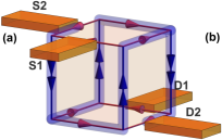
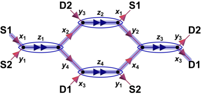
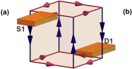
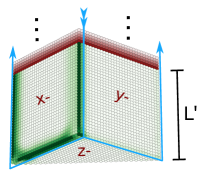
The setup we consider is shown schematically in Fig. 1. It consists of a second-order topological insulator with hinges that have one or two chiral modes, as indicated in the figure. The crystal hinges with two co-propagating chiral modes serve as beam splitters. Ohmic source and drain contacts are placed at selected crystal edges with a single chiral hinge mode, such that there are two paths connecting each pair of source and drain contacts along the crystal hinges. By controlling the phase difference between the interfering paths with a magnetic field one thereby obtains a Mach-Zehnder interferometer.
Like the chiral edge states of the integer quantized Hall effect, the hinge modes of a higher-order topological insulator are topologically protected. One distinguishes “intrinsic” hinge modes, which are protected by the topology of the bulk band structure and “extrinsic” modes, for which the nontrivial topology resides in the surface band structure, whereas the bulk may be topologically trivial [23, 24, 12]. Whereas intrinsic higher-order phases require crystalline symmetries for their protection, extrinsic topological phases do not have additional symmetry requirements. For the realization of an interferometer, all that matters is the existence of the chiral hinge modes, not where they derive their protection from. For that reason, in this article we seek a (theoretical) realization of a Mach-Zehnder interferometer in an extrinsic second-order topological insulator.
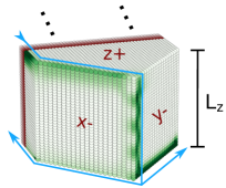
A particularly simple and controllable model of an extrinsic second-order topological insulator was proposed by Sitte et al. in Ref. [5]. It consists of a (first-order) topological insulator placed in a magnetic field at a generic direction with respect to the crystal faces, see Fig. 2. Without the magnetic field, there are Dirac-cone surface states at the crystal surfaces. The magnetic field gaps these out. This effectively turns the crystal surfaces into two-dimensional quantized Hall systems with a (half-integer) filling fraction that depends on the perpendicular component of the magnetic field and the position of the Fermi level with respect to the Dirac point of the surface band structure. The former can be controlled by the applied magnetic field, the latter by a gate voltage applied locally at the surface. The number of hinge states then follows as the difference of the filling fractions of the two adjacent surfaces. To bring about the interference pattern, one considers a small change of the magnetic field. If , changes the phases which electrons pick up while propagating along the hinges, while not affecting the number of hinge states and their properties.
The remainder of this article is organized as follows: In Sec. II we present a simple lattice model of an extrinsic second-order topological insulator as discussed above and establish that it has the phenomenology shown in Fig. 1 for a suitable choice of parameters. In Sec. III we add Ohmic contacts to crystal edges with a single chiral mode, as indicated in Fig. 1, and theoretically describe the resulting interferometer setup using scattering theory. In Sec. IV we consider a two-terminal Aharonov-Bohm interferometer based on the same model system. We conclude in Sec. V. Further details and supporting material can be found in the appendices.
II Lattice model of an extrinsic second-order topological insulator
We theoretically describe the extrinsic second-order topological insulator using a four-band lattice model with nearest-neighbor hopping [5]. It has the Hamiltonian
| (1) |
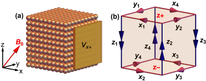
where the indices and run over all neighboring sites of a three-dimensional simple cubic lattice, and are the corresponding position vectors, , and , are four-component spinor annihilation and creation operators, and and are matrices. We consider a lattice of size , with surfaces perpendicular to the coordinate axes, shown schematically in Fig. 2. For the nearest-neighbor term we take
| (2) |
where is the lattice constant, a hopping amplitude (with the dimension of energy), and , , are Pauli matrices, and is the vector potential corresponding to the uniform applied magnetic field . The on-site term is
| (3) |
where is a parameter governing the bulk band structure and a scalar potential, which is nonzero in the vicinity of the crystal boundaries only.
Without applied magnetic field, the system has time-reversal symmetry. It is in a topological phase with gapless Dirac-cone surface states for . The surface Dirac nodes are at zero energy if the scalar potential is zero, but they may be pushed away from zero by application of uniform potential at the surface. We take a scalar potential of the form
| (4) |
where the summation index runs over all six surfaces of the crystal, is a gate voltage at surface , is the distance to the surface , and a decay length. In our calculations, we set and throughout.
A uniform magnetic field at a direction such that there is a finite flux penetrating all six crystal surfaces, gaps out the surface Dirac cones and effectively turns the surfaces into gapped quantized Hall effects. The filling fractions of the different surfaces can be tuned by varying the surface gate voltages of Eq. (4).
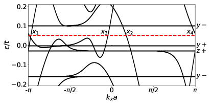
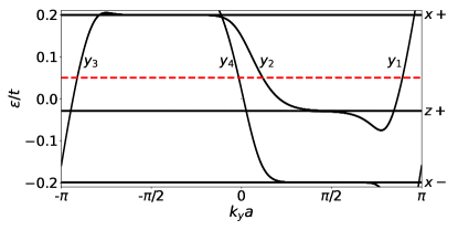
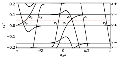
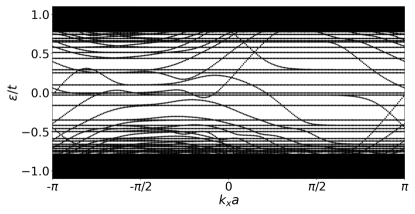
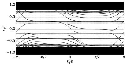
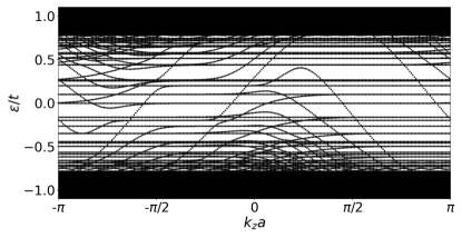
To establish that the model describes an extrinsic second-order topological insulator [5] with the configuration of hinge states shown in Fig. 1, we consider a system that is infinite along each one of the coordinate axes and calculate the corresponding band structure. Examples of such band structures in the vicinity of the Fermi energy are shown in Fig. 3. In Fig. 3 one easily recognizes the flat surface bands of the Landau levels and the dispersing one-dimensional hinge states. For these numerical calculations, the magnetic field was set to and the Fermi energy was set to (indicated by the horizontal dashed line in Fig. 3). The gate voltages are , , , , , , where we used the convention of Fig. 2 (right) to label the surfaces. Whereas the detailed band structures shown in Fig. 3 depend on the gauge choice made for the vector potential used to describe the uniform magnetic field , the numbers of hinge modes at each crystal edge, their velocities, and, if applicable, the momentum difference between co-propagating hinge modes at the same hinge do not depend on it. Band structures covering a larger range of energies are shown in App. A.
III Mach-Zehnder Interferometer
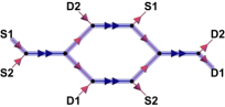
To construct a Mach-Zehnder interferometer, Ohmic contacts S1, S2, D1, and D2 are added to four of the crystal edges that support only a single chiral hinge mode, see Fig. 1. Using the labeling convention of Fig. 2 (right), these are the edges , , , and . The effective network diagram of Fig. 1 (right) is reproduced in Fig. 4, with the labels of the individual edges added.
A bias voltage is applied to the source contact S1, whereas the other three contacts are kept grounded. The current in response to the bias voltage is measured in drain contact D1. Using the Landauer-Büttiker formalism [25], the conductance may be expressed in terms of the scattering matrix of the system,
| (5) |
We note that is a matrix even for Ohmic contacts, which have many channels, because the number of channels coupling to the system is limited by the number of chiral modes at the hinge connected to the Ohmic contacts.
The scattering matrix may be expressed in terms of scattering matrices of the eight crystal corners and in terms of scattering phases accumulated along the crystal edges. Hereto we first construct scattering matrices of the four edges with two co-propagating hinge modes, , which serve as beam splitters in the interferometer network, see Fig. 4. (We refer to Fig. 2 (right) for the labeling convention for the hinges.) The beam-splitter scattering matrices are denoted , . Each of these is the product of scattering matrices and of the crystal corners of the crystal edge and a diagonal matrix containing the phases and accumulated by the two chiral modes at the edge ,
| (8) |
Arranging the rows and columns of the matrices such that the first (second) row/column corresponds to an outgoing/incoming state at an edge parallel to the () axis, we then find
| (9) |
We write the propagation phases and for propagation along the edges with two co-propagating hinge modes as
| (10) |
where is the crystal size in the direction (i.e., along the crystal edges with two co-propagating hinge modes) and is the momentum difference between the two co-propagating hinge modes at the edge . The momentum difference is gauge independent and can be obtained from the one-dimensional band structures shown in Fig. 3. It does not change under the small changes of the applied magnetic field required to observe the interference pattern, because this field scale is proportional to the sample cross section, whereas the field dependence of is on a scale proportional to the sample length . The phases , , , , , and are gauge dependent. However, the conductance depends on the combination only, which is gauge independent and depends linearly on the total magnetic flux enclosed between the two interfering paths,
| (11) |
where is the flux quantum. For the geometry of Fig. 1, one has
| (12) |
where and are the system dimensions in the and directions, respectively. Substituting Eqs. (8)–(11) into Eq. (5) one obtains the sinusoidal magnetic-field dependence of the conductance characteristic of a Mach-Zehnder interferometer.
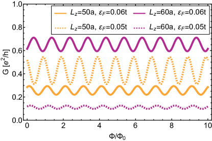
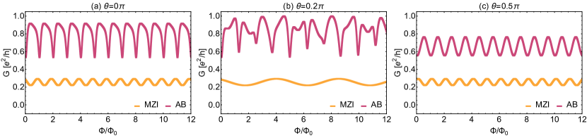
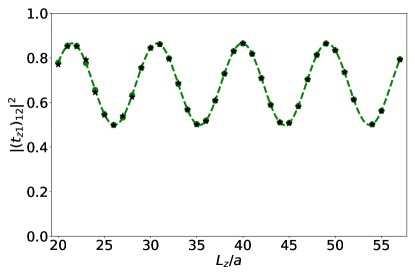
In App. B we describe how the eight scattering matrices of individual corners can be calculated for the lattice model of Sec. II using the kwant software [26], up to two magnetic-field independent over-all phase factors that can be absorbed into the propagation phases and of the crystal edges with single chiral modes. With this knowledge, the full interference pattern for the conductance can be calculated for the model of Sec. II. Examples of interference patterns for different Fermi energies and values of are shown in Fig. 5.
In a Mach-Zehnder interferometer, the interference contrast is determined by the properties of the beam splitter. For the interferometer considered here, the scattering matrices of the “beam splitters” can be manipulated externally via the momentum difference , see Eqs. (8) and (III). Small variations of may have a large effect on because of the presence of the macroscopic factors in Eq. (III). The momentum difference depends on the Fermi energy and on the gate voltages applied to the adjacent surfaces. Indeed, Fig. 5 shows different interference patterns for interferometers with different Fermi energy . Adding disorder to the system will change the particular values of the beam-spitter scattering matrices , but will not systematically affect the results or suppress the interference contrast, provided the bulk gaps remain open.
IV Two-terminal Aharonov-Bohm interferometer
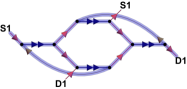
It is the presence of four Ohmic contacts in the geometry of Fig. 1 that limits the number of interfering paths between a given pair of source and drain contacts to two and, hence, leads to the characteristic sinusoidal interference pattern characteristic of a Mach-Zehnder interferometer. A two-terminal geometry, with only a single source and a single drain contact, allows for multiple interference paths and, hence, has a more complicated interference pattern. In this Section, we discuss results obtained for such a two-terminal interferometer.
A schematic of the two-terminal interferometer is shown in Fig. 6, together with an effective network diagram. In the two-terminal geometry, the conductance is still given by Eq. (5), but now is a matrix and its calculation in terms of the scattering matrices of the crystal corners and the phases accumulated along the hinges without Ohmic contacts is more involved than in the four-terminal case considered in Sec. III.
In this section we calculate the source-drain current in the two-terminal interferometer geometry. Hereto, we first define the auxiliary matrices
| (13) |
which contain the propagation amplitudes for the two paths linking the crystal edges and with each other. With this notation, the scattering matrix element describing the Mach-Zehnder interferometer with four contacts has the simple form (compare with Eq. (III))
| (14) |
In addition to the paths linking the edges and with each other, in the two-terminal geometry also loops linking the edges and to themselves are possible, see Fig. 6(b). These are described by the matrices
| (15) |
which describe loops around the faces and , respectively. With this notation, the scattering matrix element describing the Mach-Zehnder interferometer with two contacts reads
| (16) |
In order to bring about the interference patterns, it is convenient to keep the accumulated phases from the magnetic field explicit. We define , , and , where is the small shift of the magnetic field used to obtain the interference pattern, and obtain
| (17) |
with
| (18) |
where the summation is restricted to those values of for which and are non-negative and the scattering matrices are evaluated for . Eq. (17) clearly shows the possible phases contributing to the Aharonov-Bohm effect. These phases can be directly read off in the Fourier transforms of the interference patterns.
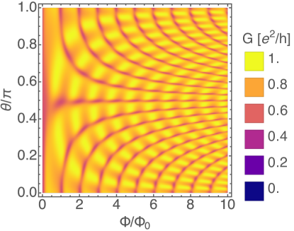
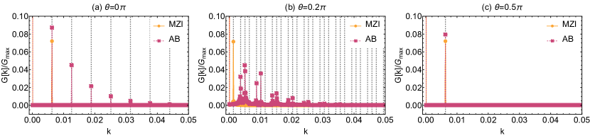
In contrast to the Mach-Zehnder interferometer of Fig. 1, for which the interference pattern depends on a single component of the magnetic field variation only, the interference pattern of the two-terminal interferometer involves the full vector . In Fig. 7 we show exemplary data for the conductance vs. for a magnetic field variation of the form , for different angles . For along a coordinate axis, i.e., or , the interference pattern of the two-terminal interferometer is periodic, but not sinusoidal. For generic the interference pattern is generically aperiodic, because periods corresponding to different interference loops are incommensurate.
For the Fourier transforms, when the magnetic field is perpendicular to the axis, one has and there is only one peak. On the other hand, for a magnetic field along , Eq. (17) predicts a flux dependence with many harmonics. In Fig. 7 of the main text and in Fig. 8 we show examples of the dependence of the two-terminal conductance on the direction of the additional field in the plane and on its strength (which is parameterized by the total flux through the three crystal faces, see Eq. (12)).
The enclosed areas can be revealed by Fourier transform to the flux . This is illustrated in Fig. 9, where we show the Fourier transform of the two-terminal and four-terminal examples used in Fig. 7.
V Conclusions and discussion
In this article we have demonstrated how to make both a Mach-Zehnder interferometer and an Aharonov-Bohm interferometer using the chiral hinge states of a three dimensional higher order topological insulator. A distinctive feature of our setup is the presence of a pair of co-propagating modes on some of the hinges, which allows the creation of beam splitters for this purpose. Ohmic contacts along specific hinges are used for the incoming and outgoing modes and, in the case of the Mach-Zehnder interferometer, for ensuring that only a single loop is available for the propagating modes.
We introduced a minimal model of the system, and solved the scattering problem for the incoming and outgoing modes at each vertex. The minimal model consists of a four band cubic system with topologically protected surface states. The application of a magnetic field and gate voltages gap out the surfaces and enable tuning of the surface topology to generate the desired configuration of hinge states. The interference patterns are calculated from the network diagram of the paths through the set-up, with scattering matrices calculated for each corner separately. This allows us to consider arbitrary system sizes, without having to sacrifice the accuracy of our numerical calculations. We performed detailed tests and comparisons of two-corner and composite single corner set-ups numerically to ensure the calculations are fully converged and under control.
The Mach-Zehnder interferometer demonstrates the expected oscillations as a function of the magnetic flux through the sample, and we further checked its dependence on applied magnetic field angle and system size. For the Aharonov-Bohm interferometer the path of the particles through the system allows for many additional loops, giving rise to very distinctive interference patterns as a function of applied magnetic field strength and direction, which serve as an experimental test of the phenomenon.
A difference with recent works [22, 21] is that the setup considered here features a crystal for which all surfaces are gapped and Ohmic contacts to hinges, whereas Refs. 22, 21 feature point contacts to surfaces with ungapped surface states, with chiral hinge modes only running along the four hinges joining these surfaces. Contacting the hinges is essential for the four-terminal Mach-Zehnder geometry we consider here. On the other hand, the interference patterns we observe for the two-terminal Aharonov-Bohm geometry are quite similar to those of Refs. 22, 21. A minor difference in this case is that the setup of Refs. 22, 21 is limited to magnetic fields parallel to the contact planes, whereas the present setup has a nontrivial interference pattern as a function of the full three dimensional magnetic field vector.
Our modeling of the interferometer involves an extrinsic higher-order topological insulator. For an extrinsic higher-order phase, the presence of chiral hinge modes relies solely on the crystal termination. In contrast, for an intrinsic higher-order topological insulator, the presence of hinge modes is imposed by the topology of the bulk band structure. Nevertheless, for intrinsic higher-order topological insulators the bulk band structure only partially fixes the number of hinge modes, so that a certain degree of control of the crystal termination remains necessary if higher-order topological insulators are to be used for interferometry purposes [5, 23, 24]. The advantage of the fully extrinsic scheme we employ here (first proposed by Sitte et al. [10]) is that the hinge modes originate from the Dirac-cone surface states of a parent first-order topological insulator state and, hence, can be controlled by standard means such as an applied magnetic field and electrostatic gate voltages.
Acknowledgements.
This work was supported by the Polish National Agency for Academic Exchange (NAWA) under the grant 2PPN/BEK/2020/1/00338/DEC/2 (NS) and by the Deutsche Forschungsgemeinschaft (DFG, German Research Foundation) - Project Number 277101999 - CRC TR 183 (project A03) (AYC and PWB).Appendix A Further Band Structures
Fig. 10 shows the band structures for a system infinite along the , , or direction for a larger energy range than shown in Fig. 3 of the main text. In this wider energy range, bulk states (the solid blocks at the top and bottom of the plots), surface landau levels (flat bands) and hinge modes (dispersing modes) are all visible.
Appendix B Corner Scattering Matrices
In order to describe arbitrarily large system sizes we characterise corners by the eight scattering matrices , , describing the scattering between hinge modes at a single corner of the crystal, see Sec. III of the main text. We can numerically obtain each of these scattering matrices for a lattice model by applying the kwant software [26] to a geometry in which there is only one corner with a nontrivial scattering matrix.
We illustrate this procedure for the calculation of the scattering matrix , which describes scattering at the lower left corner of the crystal shown in Fig. 1, which is the corner between crystal faces , , and . Figure 11 shows the geometry used to calculate this scattering matrix. It consists of a pillar with a triangular cross-section, which is semi-infinite in the direction. Three faces of the triangular pillar correspond to the crystal faces , , and , whereas the fourth, diagonal face (the back face of the pillar shown in Fig. 11) has a termination not present in the crystal of Fig. 1. The center hinge, which connects the faces and , supports a pair of modes, while the other two hinges in the direction and the hinges between the and , as well as and faces support one mode each. The triangular pillar geometry has three corners. Of these, the corner between the faces , , and (shown centrally in Fig. 11) is the corner of interest. The other two corners, which border on the diagonal face, have one incoming and one outgoing hinge mode, so that they only contribute a phase shift to the scattering state.
The triangular pillar structure has two incoming modes, propagating along the hinge between the and faces, and two outgoing modes. Hence, it is described by a scattering matrix , which can be calculated using the standard routines of the kwant software. This scattering matrix is of the form
| (19) |
where and are the wavenumbers of the two hinge modes at the hinge between and , is the size of the scattering region, and and are phase shifts accumulated for propagation along hinges and corners with a single mode. Since the wavenumbers and can be obtained from the dispersion of Fig. 3, knowledge of yields up to left multiplication with a diagonal matrix of phase factors. Not knowing this phase information is unproblematic for the calculation of the “beam-splitter” transmission matrices of Eq. (8).
We have compared building the beam-splitter scattering matrix from the corner scattering matrices and and phase shifts for propagation along the crystal hinge in between, see Eq. (8), with a direct calculation of using the kwant software. Such a direct calculation is possible by considering a “wedge-like” geometry, as shown in Fig. 11 for the calculation of the beam-splitter scattering matrix . Fig. 12 compares for the two cases and shows good agreement for a separation between the two corners.
References
- Born et al. [2019] M. Born, E. Wolf, and A. B. Bhatia, Principles of Optics: Electromagnetic Theory of Propagation, Interference, and Diffraction of Light, seventh (expanded) anniversary edition, 60th anniversary edition ed. (Cambridge University Press, Cambridge, 2019).
- Ji et al. [2003] Y. Ji, Y. Chung, D. Sprinzak, M. Heiblum, D. Mahalu, and H. Shtrikman, An electronic Mach–Zehnder interferometer, Nature 422, 415 (2003).
- Neder et al. [2007] I. Neder, N. Ofek, Y. Chung, M. Heiblum, D. Mahalu, and V. Umansky, Interference between two indistinguishable electrons from independent sources, Nature 448, 333 (2007).
- Volovik [2010] G. E. Volovik, Topological superfluid 3He-B in magnetic field and ising variable, JETP Letters 91, 201 (2010).
- Sitte et al. [2012] M. Sitte, A. Rosch, E. Altman, and L. Fritz, Topological Insulators in Magnetic Fields: Quantum Hall Effect and Edge Channels with a Nonquantized theta Term, Physical Review Letters 108, 126807 (2012).
- Zhang et al. [2013] F. Zhang, C. L. Kane, and E. J. Mele, Surface State Magnetization and Chiral Edge States on Topological Insulators, Physical Review Letters 110, 046404 (2013).
- Benalcazar et al. [2017] W. A. Benalcazar, B. A. Bernevig, and T. L. Hughes, Quantized electric multipole insulators, Science 357, 61 (2017).
- Langbehn et al. [2017] J. Langbehn, Y. Peng, L. Trifunovic, F. Von Oppen, and P. W. Brouwer, Reflection-Symmetric Second-Order Topological Insulators and Superconductors, Physical Review Letters 119, 246401 (2017).
- Song et al. [2017] Z. Song, Z. Fang, and C. Fang, (d-2) -Dimensional Edge States of Rotation Symmetry Protected Topological States, Physical Review Letters 119, 246402 (2017).
- Schindler et al. [2018a] F. Schindler, A. M. Cook, M. G. Vergniory, Z. Wang, S. S. P. Parkin, B. A. Bernevig, and T. Neupert, Higher-order topological insulators, Science Advances 4, eaat0346 (2018a).
- Fang and Fu [2019] C. Fang and L. Fu, New classes of topological crystalline insulators having surface rotation anomaly, Science Advances 5, eaat2374 (2019).
- Trifunovic and Brouwer [2021] L. Trifunovic and P. W. Brouwer, Higher-Order Topological Band Structures, physica status solidi (b) 258, 2000090 (2021).
- Xie et al. [2021] B. Xie, H.-X. Wang, X. Zhang, P. Zhan, J.-H. Jiang, M. Lu, and Y. Chen, Higher-order band topology, Nature Reviews Physics 3, 520 (2021).
- Schindler et al. [2018b] F. Schindler, Z. Wang, M. G. Vergniory, A. M. Cook, A. Murani, S. Sengupta, A. Y. Kasumov, R. Deblock, S. Jeon, I. Drozdov, H. Bouchiat, S. Guéron, A. Yazdani, B. A. Bernevig, and T. Neupert, Higher-order topology in bismuth, Nature Physics 14, 918 (2018b).
- Nayak et al. [2019] A. K. Nayak, J. Reiner, R. Queiroz, H. Fu, C. Shekhar, B. Yan, C. Felser, N. Avraham, and H. Beidenkopf, Resolving the topological classification of bismuth with topological defects, Science Advances 5, eaax6996 (2019).
- Noguchi et al. [2021] R. Noguchi, M. Kobayashi, Z. Jiang, K. Kuroda, T. Takahashi, Z. Xu, D. Lee, M. Hirayama, M. Ochi, T. Shirasawa, P. Zhang, C. Lin, C. Bareille, S. Sakuragi, H. Tanaka, S. Kunisada, K. Kurokawa, K. Yaji, A. Harasawa, V. Kandyba, A. Giampietri, A. Barinov, T. K. Kim, C. Cacho, M. Hashimoto, D. Lu, S. Shin, R. Arita, K. Lai, T. Sasagawa, and T. Kondo, Evidence for a higher-order topological insulator in a three-dimensional material built from van der Waals stacking of bismuth-halide chains, Nature Materials 20, 473 (2021).
- Aggarwal et al. [2021] L. Aggarwal, P. Zhu, T. L. Hughes, and V. Madhavan, Evidence for higher order topology in Bi and Bi0.92Sb0.08, Nature Communications 12, 4420 (2021).
- Gray et al. [2019] M. J. Gray, J. Freudenstein, S. Y. F. Zhao, R. O’Connor, S. Jenkins, N. Kumar, M. Hoek, A. Kopec, S. Huh, T. Taniguchi, K. Watanabe, R. Zhong, C. Kim, G. D. Gu, and K. S. Burch, Evidence for Helical Hinge Zero Modes in an Fe-Based Superconductor, Nano Letters 19, 4890 (2019).
- Zhang et al. [2019] R.-X. Zhang, W. S. Cole, and S. Das Sarma, Helical Hinge Majorana Modes in Iron-Based Superconductors, Physical Review Letters 122, 187001 (2019).
- Niyazov et al. [2018] R. A. Niyazov, D. N. Aristov, and V. Y. Kachorovskii, Tunneling Aharonov-Bohm interferometer on helical edge states, Physical Review B 98, 045418 (2018).
- Luo et al. [2021] K. Luo, H. Geng, L. Sheng, W. Chen, and D. Y. Xing, Aharonov-Bohm effect in three-dimensional higher-order topological insulators, Physical Review B 104, 085427 (2021).
- Li et al. [2021] C.-A. Li, S.-B. Zhang, J. Li, and B. Trauzettel, Higher-Order Fabry-Pérot Interferometer from Topological Hinge States, Physical Review Letters 127, 026803 (2021).
- Geier et al. [2018] M. Geier, L. Trifunovic, M. Hoskam, and P. W. Brouwer, Second-order topological insulators and superconductors with an order-two crystalline symmetry, Physical Review B 97, 205135 (2018).
- Trifunovic and Brouwer [2018] L. Trifunovic and P. Brouwer, Higher-order bulk-boundary correspondence for topological crystalline phases, Physical Review X 9, 11012 (2018).
- Büttiker [1986] M. Büttiker, Four-Terminal Phase-Coherent Conductance, Physical Review Letters 57, 1761 (1986).
- Groth et al. [2014] C. W. Groth, M. Wimmer, A. R. Akhmerov, and X. Waintal, Kwant: A software package for quantum transport, New Journal of Physics 16, 063065 (2014).