Observation of anisotropic Dirac cones in the topological material Ti2Te2P
Abstract
Anisotropic bulk Dirac (or Weyl) cones in three dimensional systems have recently gained intense research interest as they are examples of materials with tilted Dirac (or Weyl) cones indicating the violation of Lorentz invariance. In contrast, the studies on anisotropic surface Dirac cones in topological materials which contribute to anisotropic carrier mobility have been limited. By employing angle-resolved photoemission spectroscopy and first-principles calculations, we reveal the anisotropic surface Dirac dispersion in a tetradymite material Ti2Te2P on the (001) plane of the Brillioun zone. We observe the quasi-elliptical Fermi pockets at the -point of the Brillouin zone forming the anisotropic surface Dirac cones. Our calculations of the indices confirm that the system is topologically non-trivial with multiple topological phases in the same material. In addition, the observed nodal-line like feature formed by bulk bands makes this system topologically rich.
The experimental discovery of a three-dimensional (3D) topological insulator (TI) in tetradymite Bi2Se3 brought about an unprecedented surge of research interests in exotic states of matter [1, 2, 3, 5, 6, 7, 8, 4]. This discovery motivated investigations of other novel phases such as the Dirac semimetal, Weyl semimetal, nodalline semimetal, topological crystalline insulator, Kondo insulator, etc [9, 10, 11, 12, 13, 14, 15, 16, 17, 18]. Not only have the discoveries of these novel states provided new classifications of materials, but a series of compounds with similar electronic behaviors have also been identified. Recently, a great deal of interest has been directed at a series of bismuth- and antimony-based tetradymite crystals as they host a topological surface state while simultaneously possessing a wide bulk band gap, as such a single 2D Dirac cone in the Brillouin zone (BZ) is present [6, 7, 21, 23, 22, 24, 25, 26, 19, 20, 27]. Similarly, angle-resolved photoemission spectroscopy (ARPES) studies of the 221-type compounds isostructural to the tetradymite family such as Zr2Te2P, and Hf2Te2P [28, 29, 30] reveal the presence of topological surface states along with multiple fermionic-states in the BZ. In Zr2Te2P, multiple Dirac cones are reported, among which two Dirac cones reside within the pseudo gap. Additionally, it contains a surface state anisotropic Dirac cone at the point [28]. Another compound of this family, Hf2Te2P, possesses multiple topological states, hosting strong TI and weak TI states in a single material. Furthermore, it consists of a one-dimensional Dirac-node arc along a high symmetry direction which makes this family even more fascinating [30]. Interestingly, the band inversion takes place between the d and p bands in these compounds in contrast to other tetradymite families which host band inversion between s and p bands or between p bands [27, 28, 29, 30, 31].
Most of the well studied TIs and topological semimetals (TSMs) have isotropic Dirac cones which are dubbed as type-I fermions. Bi2Se3, Cd3As2 and TaAs are prime examples of materials hosting type-I fermions in TI, Dirac and Weyl semimetallic states, respectively [6, 10, 13]. However, very recently topological states with tilted Dirac cones have gained significant attention. Subsequently, type-II Weyl semimetal [32] and type-II Dirac semimetals [33, 34, 35] have been discovered in three dimensional systems. These anisotropic Dirac cones are formed by bulk bands. Type-II fermions have tilted Dirac cones as a result of broken Lorentz invariance, and Dirac or Weyl nodes exist at the contact of electron and hole energy pockets [32]. In a similar fashion, anisotropic Dirac cones have been reported in two dimensional systems in which Fermi velocities vary along high symmetry directions [36, 37, 38]. The anisotropy of the Dirac cone might provide anisotropic carrier mobility, thus leading to the realization of direction-dependent transport for quantum devices [36, 38]. A few materials harboring anisotropic surface Dirac cones have been reported [39, 40, 41, 28, 42, 43]. However, the examples of 2D anisotropic Dirac cones are limited in 3D materials.
In this work, we investigate the electronic band structures of the (001) surface of Ti2Te2P using high-resolution vacuum ultraviolet ARPES and first-principles calculations. Our measurements reveal the presence of anisotropic surface Dirac cones at the point and nodal-line-like features along the - direction. The experimental results are in excellent agreement with the first-principles calculations. Parity calculations reveal the band-inversions at the and the F point indicating that the system is topologically rich. The anisotropic Dirac cones have the potential to be used in technological applications due to the different mobilities in a Dirac cone.
Single crystals of Ti2Te2P were grown by chemical vapor transport method as described in Ref. [1, 2], and details of sample characterizations are described in the Supplemental Material (SM) note 1 [46].
Synchrotron-based ARPES measurements were performed at the Advanced Light Source (ALS) beamline 10.0.1 equipped with Scienta R4000, ALS beamline 4.0.3 equipped with R8000 hemispherical electron analyzers, and at the SIS-HRPES end-station at the Swiss Light Source (SLS) equipped with Scienta R4000. Similarly, helium lamp based ARPES measurements were performed at the Laboratory for Advanced Spectroscopic Characterization of Quantum Materials (LASCQM) with R3000 hemispherical analyzer at University of Central Florida. The angular and energy resolutions were set to be better than 0.2∘ and 20 meV, respectively. The electronic structure calculations and structural optimization were carried out within the density-functional formalism, which are described in SM Note 2 [46, 3, 4, 5, 6, 7].
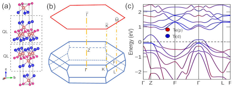
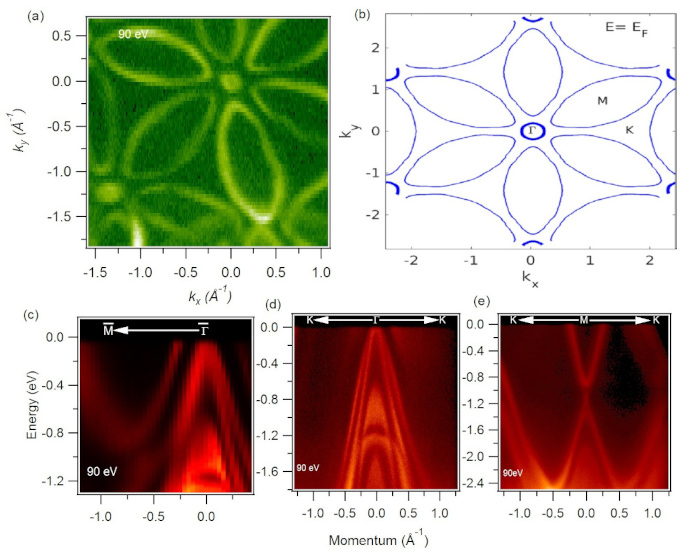
We begin our discussion by presenting the crystal structure of Ti2Te2P in Fig. 1(a
). It is isostructural to the Bi2Te2Se, which crystallizes in a rhombohedral crystal structure
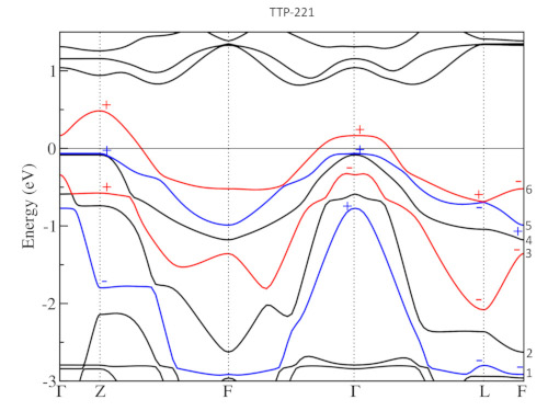
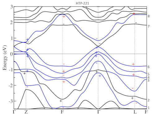
with lattice parameter a = 3.6387(2) Å, c = 28.486(2) Å and space group (No. 166), each unit cell consisting of three quintuple atomic layers separated by van der Waals gaps [1]. The phosphorus and tellurium atoms are arranged in hexagonal layers stacked along the hexagonal c-axis in a sequence with two layers of tellurium followed by a single layer of phosphorus and the gap is filled by titanium as shown in Fig. 1(a). The (001) plane is the natural cleaving plane in this compound due to the atomic layers along the c-axis. A three dimensional BZ and its projection to 2D along the [001] direction are presented in Fig. 1(b), which illustrates the hexagonal symmetry of the (001) surface BZ. Figure 1(c) shows the bulk band calculation of Ti2Te2P (with spin-orbit coupling (SOC)) along the high symmetry directions which includes four time reversal invariant momenta (TRIM) points. It shows a hole-like band around the point. A band is seen crossing the chemical potential at the point indicating the semimetallic behavior, which is flat in the vicinity of the Fermi level at the point. Our detailed electronic structures calculations show the occurrence of bulk band inversion both at the and the F point. These band inversions are between Ti-p and Te-d states and involve different sets of bands (see SM [46]). A bulk band inversion at the point takes place between
Ti p and Te d bands around 750 meV below the Fermi level,
which agrees well with both the calculated and observed
Dirac surface state at the point. This surface state is of
the strong TI type, since our calculated indices for this case are
(1;000) (see SM [46]). Unlike the other sister compounds of this family (Zr2Te2P, Hf2Te2P), Ti2Te2P does not possess band inversion above the chemical potential at the zone center. The parity analysis of this system shows that a strong TI state exist at the point and at the point (see SM for the parity calculation [46]). Our calculations indicate that the band inversion between different bulk bands at the point also leads to strong TI topology with again (1;000). Remarkably, this band inversion takes place near a similar binding energy as the one responsible for the Dirac surface state at the point (see [46]).
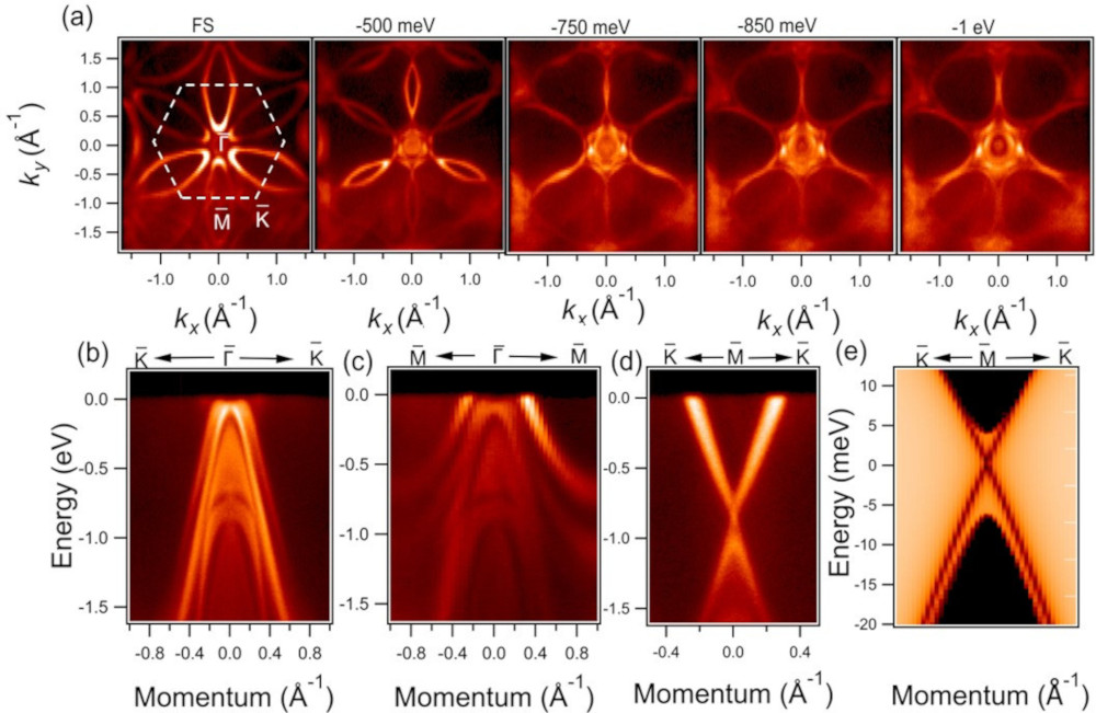
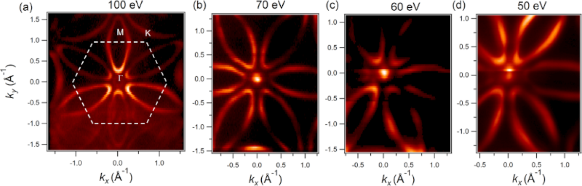
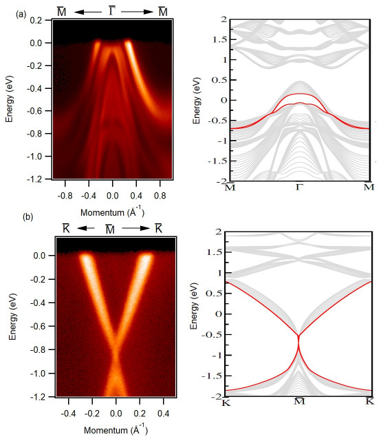
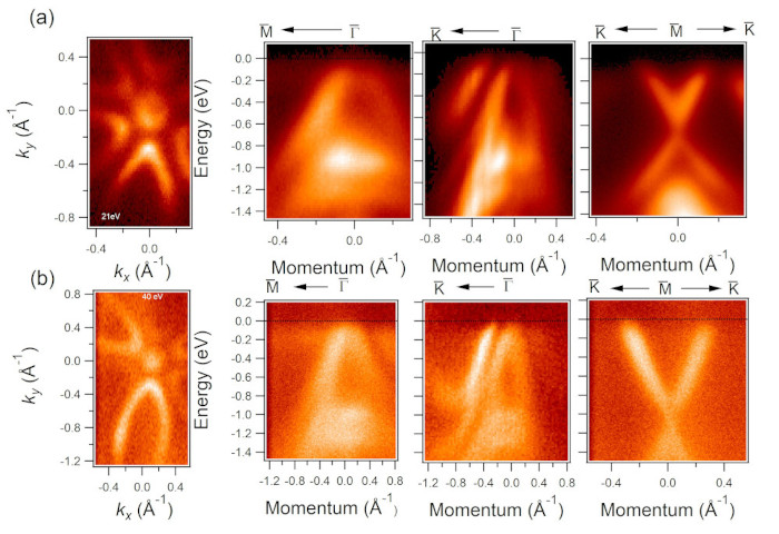
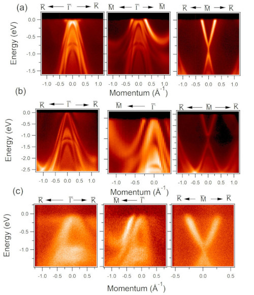
Figure 2 illustrates the detailed electronic structures of experimentally measured Ti2Te2P by using synchrotron based high resolution ARPES. In Fig. 2(a), the Fermi surface map is presented which has a six-fold flower petal shape as a consequence of the presence of the three-fold rotational and inversion symmetry. At the point, a circular-shaped energy pocket can be seen due to the hole-like band that crosses the chemical potential. Furthermore, a constructed BZ is presented in which high-symmetry points are labeled. The photoemission spectra obtained from ARPES measurements suggests that petal shaped Fermi pockets are surface originated as they do not disperse significantly with photon energies (see SM [46]). The impacts of the matrix elements effects are noticeable leading to non-uniform spectral intensities. Furthermore, petal-like features coming from the secondary BZ can be observed at the edges. The ARPES measured Fermi surface of Ti2Te2P is similar to Fermi-surface of the Zr2Te2P and Hf2Te2P [28, 29, 30]. The energy contours delineate how the band dispersions evolve with the binding energies. The energy pockets at the point grow bigger with binding energy indicating the hole nature of the bands at the point. This hexagonal BZ has six -points at the center of the elliptical Fermi pockets. The diameters of the elliptical petal diminish with binding energies. At the binding energy of 750 meV, the elliptical features collapse into lines. Furthermore, the line-like feature seen along the - direction form nodal-line-like states as it is the crossing point of bulk Dirac dispersions (see SM [46]). Interestingly, there are an even number of topological nontrivial surface states at the point and one at the point, which provide the condition for Dirac-node arcs [30]. However, we do not observe gapped bulk Dirac cones in the vicinity of the as seen in Hf2Te2P, probably due to weaker spin-orbit coupling, or due to energy resolution limitations obscuring the gap in the photoemission intensity plot. The node arc feature is protected by in-plane time-reversal invariance similar to its sister compound Hf2Te2P. In order to study the dispersion maps along high symmetry axes, we present ARPES measurements of energy dispersion along high symmetry directions. Figure 2(b) shows band structures along the -- direction. Hole-like bands are seen in the vicinity of the Fermi level. Another band exists almost 750 meV below the Fermi level, which can be seen in the bulk band calculations. Figure 2(c) displays the dispersion map along the --, in which hole-like bands can be seen. The slab calculations (see SM [46]) suggest that most of the bands are bulk originated, whereas a pair of surface originated bands are buried within bulk bands.
In Fig. 2(d), we present the dispersion map along the -- direction in which, we observe a Dirac state at the binding energy of 750 meV. Our photon energy dependent measurements suggest the surface-originated Dirac cone, however the slab calculations (see Fig. 2(e)) suggests the presence of bulk bands. The bulk bands and surface bands, however, cannot be resolved in the present resolution.
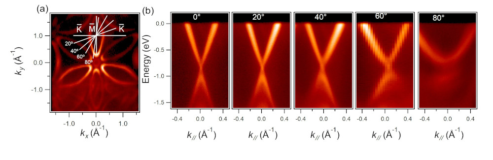
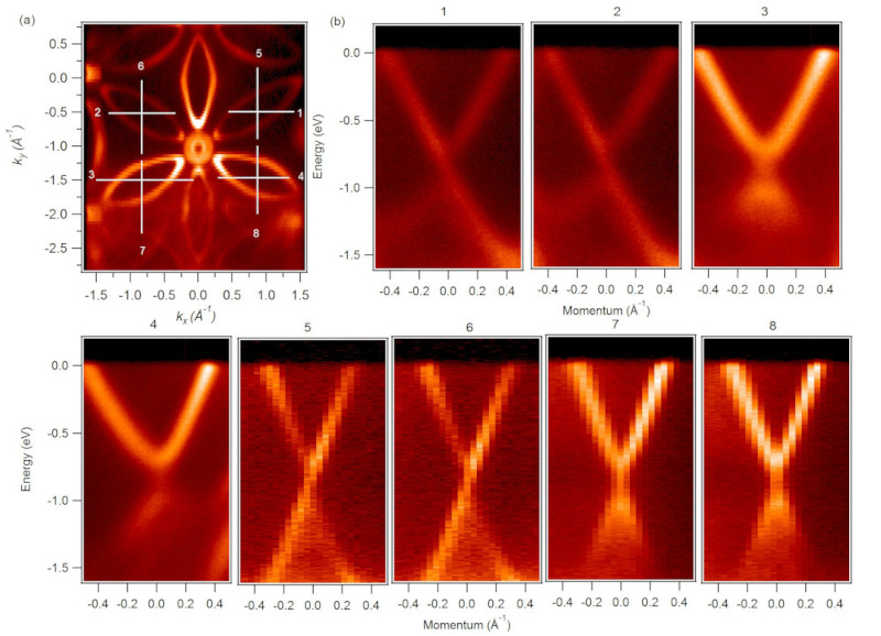
To show the anisotropic Dirac cones at the points, we have taken dispersion maps along the different directions at the point which have different Fermi velocities. Figure 3(a) shows the Fermi surface map in which one point is chosen as a reference point to demonstrate the anisotropy of the Dirac state at the point. The Dirac cones are formed by the elliptical shaped petals at the Fermi surface. In Fig. 3(b), dispersion maps along the different directions are presented, which make angles of 0∘-80∘ at an interval of 20∘. The dispersion maps delineate the presence of anisotropic Dirac cones.
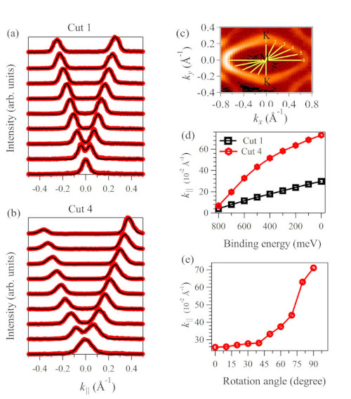
To quantitatively determine the anisotropy of the Dirac cone in Ti2Te2P, we have performed a detailed analysis along both cut 1 i.e, along the -- high-symmetry direction and cut 6 which is rotated 60∘ with respect to the -- direction [see Figs. 4(a)-4(c)]. Figures 4(a)-4(b) show the momentum distribution curves (MDCs)(red open circles) which are extracted from the ARPES dispersions. In order to fit the obtained MDCs, Gaussian-Lorentzian (GL) product functions have been used. The Gaussian part represents primarily the energy resolution of the instrument and the lifetime broadening of the photoelectrons, whereas the core holes are captured by the Lorentzian width [52, 53]. The fitted MDCs as shown in Figs. 4a-b show accurate fits upto around 750 meV i.e, near the Dirac point. From the obtained results one can see that along cut 1, the dispersion of the topological surface states (TSSs) follows a linear behavior whereas along cut 4 the dispersion of the TSS deviated quite strongly from the linear behavior (see Fig. 4(d)). The different behavior of the dispersion of the TSS along the different directions thus clearly shows the anisotropic dispersion of the TSS. The magnitude of the Fermi velocity associated with cut 1 is almost double of cut 4.
Fig. 4(e) displays the change in the k|| vector as a function of the rotation angle where the rotation has been performed with respect to the high symmetry direction --; it clearly shows a significant increase of the k|| wave vector above 40∘ rotation.
The anisotropic surface Dirac cone in a 3D system has been overlooked despite substantial works done on the tilted bulk Dirac cones in semimetallic systems.
The anisotropic Dirac cone at the point of Ti2Te2P is the consequence of the petal shaped energy pocket at the point in the BZ, due to which the Fermi velocities vary along the directions of the dispersion maps. The anisotropy of TSSs in some materials have been observed [54, 7, 55, 56, 43, 41], which are attributed to the spin-dependent scattering giving rise to anisotropic scattering rates of the surface-state electrons, however the role of spin-dependent scattering in Ti2Te2P is yet to be revealed. Importantly, materials with anisotropic surface Dirac cones could be a platform that provide a direction dependent transport. It requires further explorations in such materials.
In conclusion, we observe anisotropic Dirac cones at the points in Ti2Te2P material. Our calculations identify this system as topologically non-trivial. The presence of nodalline like features along the - direction in addition to the anisotropic Dirac cones makes this system topologically rich. Our study provides an archetype system for the understanding of the 221-tetradymite system and we anticipate that it will stimulate further research interests in this class of materials.
M.N. acknowledges support from the Air Force Office of Scientific
Research under Award No. FA9550-17-1-0415, the
Air Force Office of Scientific Research MURI (Grant
No. FA9550-20-1-0322), and
the National Science Foundation (NSF) CAREER award
DMR-1847962. A.K.N., A.A., and P.M.O. acknowledge support from the Swedish Research Council (VR) and from the Knut and Alice Wallenberg Foundation (Grant No. 2015.0060). Computational resources were provided by the Swedish National Infrastructure for computing (SNIC)(Grant No. 2018-05973). A. K. N. acknowledges the support of Department of Atomic Energy (DAE) and Science and Engineering Research Board (SERB) research grant (Grant No. SRG/2019/000867) of the Government of India. We thank Sung-Kwan Mo and Jonathan Denlinger for beamline assistance at the LBNL. This research used resources of the Advanced Light Source, a U.S. DOE Office of Science User Facility under contract no. DE-AC02-05CH11231. We thank Nicholas
Clark Plumb for beamline assistance at the SLS, PSI.
∗ Corresponding author: Madhab.Neupane@ucf.edu
References
- [1] M. Z. Hasan and C. L. Kane, Rev. Mod. Phys. 82, 3045 (2010).
- [2] X.-L. Qi and S.-C. Zhang, Rev. Mod. Phys. 83, 1057(2011).
- [3] M. Z. Hasan, S.-Y. Xu, and M. Neupane, Topological Insulators, Topological Dirac semimetals, Topological Crystalline Insulators, and Topological Kondo Insulators. in Topological Insulators: Fundamentals and Perspectives eds Ortmann F., Roche S., Valenzuela S. O. John Wiley & Sons (2015).
- [4] A. Bansil, H. Lin, T. Das, Rev. Mod. Phys. 88, 021004-021037 (2016).
- [5] L. Fu, C. L. Kane, E. J. Mele, Phys. Rev. Lett. 98, 106803 (2007).
- [6] Y. Xia, D. Qian, D. Hsieh, L. Wray, A. Pal, H. Lin, A. Bansil, D. Grauer, Y. S. Hor, R. J. Cava, and M. Z. Hasan, Nat. Phys. 5, 398 (2009).
- [7] Y. L. Chen, J. G. Analytis, J.-H. Chu, Z. K. Liu, S.-K. Mo, X. L. Qi, H. J. Zhang, D. H. Lu, X. Dai, Z. Fang, S. C. Zhang, I. R. Fisher, Z. Hussain, and Z.-X. Shen, Science , 178 (2009).
- [8] Y. Ando, and L. Fu, Annu. Rev. Condens. Matter Phys. , 361 (2015).
- [9] Z. Wang, H. Weng, Q. Wu, X. Dai, and Z. Fang, Phys. Rev. B 88, 125427 (2013).
- [10] M. Neupane, S.-Y. Xu, R. Sankar, N. Alidoust, G. Bian, C. Liu, I. Belopolski, T.-R. Chang, H.-T. Jeng, H. Lin, A. Bansil, F. Chou, and M. Z. Hasan, Nat. Commun. , 3786 (2014).
- [11] B.-J. Yang and N. Nagaosa, Nat. Commun. 5, 4898 (2014).
- [12] S. M. Young, S. Zaheer, J. C. Y. Teo, C. L. Kane, E. J. Mele, and A. M. Rappe, Phys. Rev. Lett. 108, 140405 (2012).
- [13] S.-Y. Xu, I. Belopolski, N. Alidoust, M. Neupane, G. Bian, C. Zhang, R. Sankar, G. Chang, Z. Yuan, C.-C. Lee et al., Science 349, 613 (2015).
- [14] H. Weng, C. Fang, Z. Fang, B. A. Bernevig, X. Dai, Phys. Rev. X 5, 011029 (2015).
- [15] M. Neupane, I. Belopolski, M. M. Hosen, D. S. Sanchez, R. Sankar, M. Szlawska, S.-Y. Xu, K. Dimitri, N. Dhakal, P. Maldonado et al., Phys. Rev. B 93, 201104(R) (2016).
- [16] M. M. Hosen, K. Dimitri, I. Belopolski, P. Maldonado, R. Sankar, N. Dhakal, G. Dhakal, T. Cole, P. M. Oppeneer, D. Kaczorowski et al., Phys. Rev. B 95, 116101(R) (2017).
- [17] L. Fu, Phys. Rev. Lett. 106, 106802 (2011).
- [18] M. Neupane, N. Alidoust, S. Y. Xu, T. Kondo, Y. Ishida, D. J. Kim, C. Liu, I. Belopolski, Y. J. Jo, T. R. Chang et al., Nat. Commun. 4, 2991(2013).
- [19] M. Neupane, S. Basak, N. Alidoust, S. Y. Xu, C. Liu, I. Belopolski, G. Bian, J. Xiong, H. Ji, S. Jia et al., Phys. Rev. B , 165129 (2013).
- [20] S.-Y. Xu, M. Neupane, C. Liu, D. Zhang, A. Richardella, L. Andrew Wray, N. Alidoust, M. Leandersson, T. Balasubramanian, J. Sánchez-Barriga et al., Nat. Phys. , 616 (2012).
- [21] Z. Ren, A. A. Taskin, S. Sasaki, K. Segawa, and Y. Ando, Phys. Rev. B , 241306 (R) (2010).
- [22] H. Ji, J. M. Allred, M. K. Fuccillo, M. E. Charles, M. Neupane, L. A. Wray, M. Z. Hasan, and R. J. Cava, Phys. Rev. B , 201103(R) (2012).
- [23] C. Pauly, G. Bihlmayer, M. Liebmann, M. Grob, A. Georgi, D. Subramaniam, M. R. Scholz, J. Sánchez-Barriga, A. Varykhalov, S. Blügel, O. Rader, and M. Morgenstern, Phys. Rev. B 86, 235106 (2012).
- [24] C.-K. Lee, C.-M. Cheng, S.-C. Weng, W.-C. Chen, K.-D. Tsuei, S.-H. Yu, M. M.-C. Chou, C.-W. Chang, L.-W. Tu, H.-D. Yang, C.-W. Luo, and M. M. Gospodinov, Sci. Rep. 6, 36538 (2016).
- [25] J. E. Moore, Nature , 194-198 (2010).
- [26] M. Neupane, A. Richardella, J. Sánchez-Barriga, S. Xu, N. Alidoust, I. Belopolski, C. Liu, G. Bian, D. Zhang, D. Marchenko et al., Nat. Commun. 5, 3841 (2014).
- [27] H. J. Zhang, C. X. Liu, X. L. Qi, X. Dai, Z. Fang, and S. C. Zhang, Nat. Phys. 5, 438 (2009).
- [28] H. Ji, I. Pletikosić, Q. D. Gibson, G. Sahasrabudhe, T. Valla, and R. J. Cava, Phys. Rev. B 93, 045315 (2016).
- [29] K. W. Chen, N. Aryal, J. Dai, D. Graf, S. Zhang, S. Das, P. Le Fèvre, F. Bertran, R. Yukawa, K. Horiba et al., Phys. Rev. B 97, 165112 (2018).
- [30] M. M. Hosen, K. Dimitri, A. K. Nandy, A. Aperis, R. Sankar, G. Dhakal, P. Maldonado, F. Kabir, C. Sims, F. Chou et al., Nat. Commun. 9, 3002 (2018).
- [31] J. Dai, E. Frantzeskakis, N. Aryal, K.-W. Chen, F. Fortuna, J. E. Rault, P. Le Fèvre, L. Balicas, K. Miyamoto, T. Okuda, E. Manousakis, R. E. Baumbach, A. F.Santander-Syro, Phys. Rev. Lett. 126, 196407(2021).
- [32] A. A. Soluyanov, D. Gresch, Z. Wang, Q. Wu, M. Troyer, X. Dai, and B. A. Bernevig, Nature (London) 527, 495 (2015).
- [33] H. Huang, S. Zhou, and W. Duan, Phys. Rev. B 94, 121117 (R) (2016).
- [34] C. Le, S. Qin, X. Wu, X. Dai, P. Fu, Chen Fang, and J. Hu, Phys. Rev. B 96, 115121(2017).
- [35] T.-R. Chang, S.-Y. Xu, D. S. Sanchez, W.-F. Tsai, S.-M. Huang, G. Chang, C.-H. Hsu, G. Bian, I. Belopolski, Z.-M. Yu et al., Phys. Rev. Lett. 119, 026404(2017).
- [36] B. Feng, J. Zhang, S. Ito, M. Arita, C. Cheng, L. Chen, K. Wu, F. Komori, O. Sugino, K. Miyamoto et al., Adv. Mater. 30, 1704025 (2018).
- [37] H.-Y. Lu, A. S. Cuamba, S.-Y. Lin, L. Hao, R. Wang, H. Li, Y. Zhao, and C. S. Ting, Phys. Rev. B 94, 195423 (2016).
- [38] Y. Zhao, X. Li, J. Liu, C. Zhang, and Q. Wang, J. Phys. Chem. Lett. 9, 1815 (2018).
- [39] J. Park, G. Lee, F. Wolff-Fabris, Y. Y. Koh, M. J. Eom, Y. K. Kim, M. A. Farhan, Y. J. Jo, C. Kim, J. H. Shim, and J. S. Kim, Phys. Rev. Lett. 107, 126402 (2011).
- [40] B. Feng, J. Zhang, S. Ito, M. Arita, C. Cheng, L. Chen, K. Wu, F. Komori, O. Sugino, K. Miyamoto et al., Sci. Rep. 4, 5385 (2014).
- [41] Q. D. Gibson, D. Evtushinsky, A. N. Yaresko, V. B. Zabolotnyy, M. N. Ali, M. K. Fuccillo, J. Van den Brink, B. Büchner, R. J. Cava, and S. V. Borisenko, Sci. Rep. 4, 5168 (2014).
- [42] F. Virot, R. Hayn, M. Richter, and J. van den Brink, Phys. Rev. Lett. 106, 236806 (2011).
- [43] W. Zhang, R. Yu, W. Feng, Y. Yao, H. Weng, X. Dai, and Z. Fang, Phys. Rev. Lett. 106, 156808 (2011).
- [44] F. Philipp, P. Schmidt, M. Ruck, W. Schnelle, and A. Isaeva, J. Solid State Chem. , 2859 (2008).
- [45] J. S. Oh, H.-S. Yu, C.-J. Kang, S. Sinn, M. Han, Y. J. Chang, B.-G. Park, K. Lee, B. I. Min, S. W. Kim, H.-D. Kim, and T. W., Chem. Mater. , 7570 (2016).
- [46] See Supplemental Materials for photon energy dependent measurements, different direction dispersion maps, constant energy contours etc.
- [47] G. Kresse and J. Furthmüller, Phys. Rev. B. 54, 11169–11186 (1996).
- [48] G. Kresse, and J. Furthmüller, Comput. Mater. Sci. 6, 15–50 (1996).
- [49] J. P. Perdew, K. Burke, and M. Ernzerhof, Phys. Rev. Lett. 77, 3865–3868 (1996).
- [50] G. Kresse, and D. Joubert, Phys. Rev. B 59, 1758–1775 (1999).
- [51] P. E. Blöchl, Phys. Rev. B 50, 17953–17979(1994).
- [52] T. Valla, A. V. Fedorov, P. D. Johnson, B. O. Wells, S. L. Hulbert, Q. Li, G. D. Gu, N. Koshizuka, Science 285, 2110 (1999).
- [53] T. Valla, Z.-H. Pan, D. Gardner, Y. S. Lee, and S. Chu Phys. Rev. Lett. 108, 117601 (2012).
- [54] K. Kuroda, M. Arita, K. Miyamoto, M. Ye, J. Jiang, A. Kimura, E. E. Krasovskii, E. V. Chulkov, H. Iwasawa, T. Okuda et al., Phys. Rev. Lett. 105, 076802 (2010).
- [55] S. Souma, K. Kosaka, T. Sato, M. Komatsu, A. Takayama, T. Takahashi, M. Kriener, K. Segawa, and Y. Ando, Phys. Rev. Lett. 106, 216803 (2011).
- [56] J. Sánchez-Barriga, M. R. Scholz, E. Golias, E. Rienks, D. Marchenko, A. Varykhalov, L. V. Yashina, and O. Rader, Phys. Rev. B. 90, 195413 (2014).
Supplementary Materials
Supplementary Note 1: Synthesis and bulk characterization of Ti2Te2P crystals
Single crystals of Ti2Te2P were grown by the standard chemical vapor transport method. The obtained crystals were thin platelets with typical dimensions 0.5 0.5 0.06 mm3. They had dark metallic luster and were found moderately stable against air and moisture. Their chemical composition was checked by energy-dispersive X-ray analysis ( EDAX) using an FEI scanning electron microscope equipped with an EDAX Genesis XM4 spectrometer. Results confirmed that the material is homogeneous single-phase with the stoichiometry close to the nominal one (see Fig. S1). The crystal structure was verified by single crystal X-ray diffraction performed on a Kuma-Diffraction KM4 four-circle diffractometer equipped with a CCD camera using Mo K radiation.
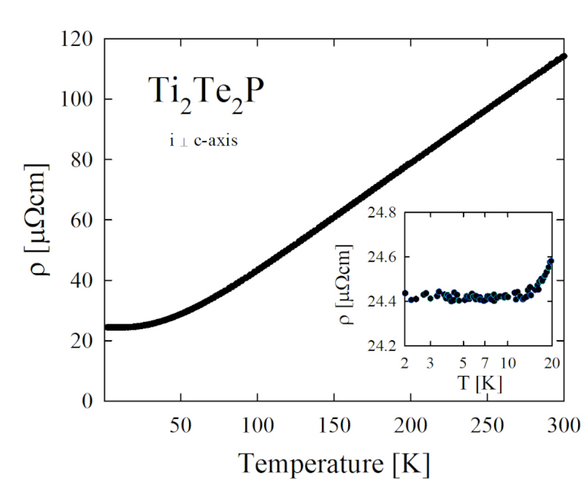
The results confirmed the rhombohedral space group Rm, and yielded the lattice parameters similar to those reported in the literature [1, 2]. Electrical resistivity measurements were carried out within the temperature range of 2-300 K using a conventional four-point ac technique implemented in a Quantum Design PPMS platform. The electrical contacts to as-grown crystals were prepared using silver epoxy paste. The electrical resistivity was measured with electrical current flowing within the hexagonal plane of the Ti2Te2P crystal lattice.
Figure S2 shows the temperature dependence of the electrical resistivity of single-crystalline Ti2Te2P, measured within the hexagonal plane of the crystallographic unit cell. The compound exhibits metallic characteristics in regards to electrical transport, in concert with the previous report [2]. However, at the lowest temperatures, the resistivity saturates at a constant value that can be associated with the residual scattering of conduction electrons on structural imperfections, at odds with the observation in Ref. [2] of a logarithmic upturn below 7 K that was attributed to weak localization or electron-electron interaction. Here, it should be noted that the specimen investigated in Ref. [2] was an ultra-thin flake exfoliated from a bulk crystal using the scotch type method, while in the present case it was a parallelepiped cut from a larger single-crystalline piece. The different form of the samples explains the discrepancy in the magnitude of the resistivity measured at room temperature (ca. 114 versus 30 -cm, in the present study and Ref. [2], respectively) and at 2 K (ca. 24.4 versus 3.5 -cm, respectively). Furthermore, it clarifies the absence in the resistivity data displayed in the inset to Fig. S2 of any clear features due to quantum corrections.
Supplementary Note 2: First-principles calculations of Ti2Te2P
Structural optimization was carried out within the density-functional formalism as implemented in the Vienna ab initio simulation package (VASP) [3, 4]. Exchange and correlation were treated within the generalized gradient approximation (GGA) using the parametrization of Perdew, Burke, and Ernzerhof (PBE) [5]. The projector augmented wave (PAW) method [6, 7] was employed for the wave functions and pseudo potentials to describe the interaction between the ion cores and valence electrons. The lattice constants and atomic geometries were fully optimized and obtained by minimization of the total energy of the bulk system. The surface of the 2D crystal was simulated as a slab calculation within the supercell approach with sufficiently thick vacuum layers. In addition to the general scalar-relativistic corrections in the Hamiltonian, the spin-orbit interaction was taken into account. The plane wave cutoff energy and the k-point sampling in the BZ integration were checked carefully to assure the numerical convergence of self-consistently determined quantities.
Supplementary Note 3: Surface and bulk bands in Ti2Te2P
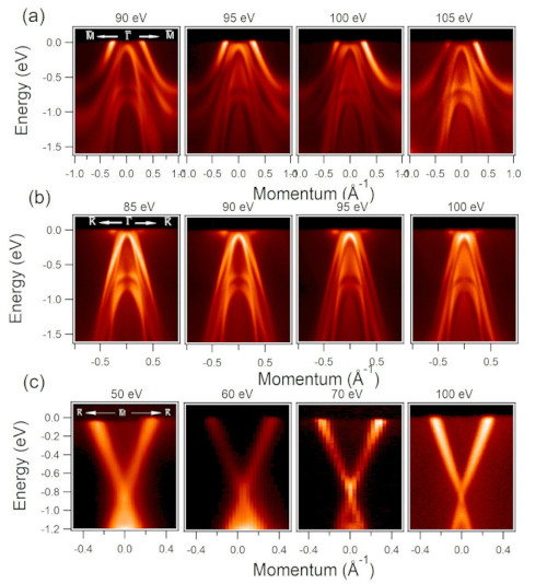
Fermi surface maps at different photon energies confer an opportunity to study the surface nature of the Fermi pockets. Surface bands do not disperse with the photon energy. In Fig. S3, it is evident that the petal-like energy pockets do not change their shape and size with change in photon energies which indicates that the bands originate from the surface. Figure S4 illustrates the ARPES measured dispersion maps and their corresponding slab calculations along the high symmetry directions -- (Fig. S4(a)) and -- (Fig. S4(b)), respectively. In the vicinity of the point as shown in Fig. S4(a), a pair of hole-like surface bands is present along with bulk bands. One band crosses the Fermi level, whereas, other bands remain below the Fermi level. Ultimately, they merge at a certain -point between the and the point to become a single band. Unlike other sister compounds of this family, it does not have a topological insulating state above the Fermi level.
As discussed in the main text, the anisotropic Dirac cone is clearly seen on the theoretical plot shown in Fig. S4(b) right panel. The upper Dirac cone extends upto 750 meV above the Fermi level.
Photon energy dependent dispersion maps along the high symmetry directions are presented in Fig. S5. It suggests that a surface state is seen at the point (see Fig. S5(c)).
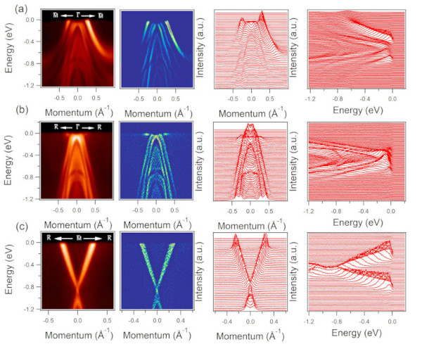
We present second derivatives, momentum distribution curves ( MDCs), Energy distribution curves ( EDCs) of dispersion maps along the high symmetry directions in Fig. S6 which provide the visualization of the bands in the respective directions.
Supplementary Note 4: Anisotropic Dirac cones
As seen in the main text, the Fermi velocity varies on the direction with respect to the -- direction. Here, we show how Fermi velocities vary when they make angles of 60∘ and 30 ∘ with respect to the -- direction (see Fig. S7). We take different points and show how the dispersion maps evolve with the angles. The slopes of each dispersion map that makes 60∘-angles with -- should have the same magnitude, however, matrix elements effects change the value to some extent. Nevertheless, anisotropic behaviors are clearly seen.
Supplementary Note 5: Observation of Dirac node-arc
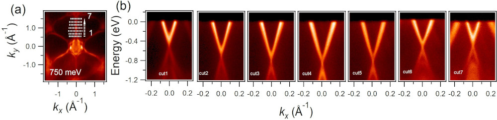
Observation of Dirac node-arc is presented in Fig. S8; we take 7 cuts in equal intervals perpendicular to the - direction. Figure S8(b) shows the evidence of Dirac node-arc as all the dispersion maps show Dirac dispersions. The Dirac node-arc extends over more than 1 in the -space.
Supplementary Note 6: Electronic structures of Hf2Te2P and Zr2Te2P
In order to investigate the electronic structures of sister compounds of Ti2Te2P, we present electronic structures of Hf2Te2P and Zr2Te2P and compare them with Ti2Te2P in Figs. S9-S11. ARPES spectra show similar Fermi maps, however, they are topologically different as a consequence of spin-orbit coupling strength. Furthermore, Dirac points are located at different binding energies. In Fig. S9, the Fermi map and dispersion maps along high symmetry direction are presented. Even though many features are similar to Ti2Te2P, some distinct features are seen in Hf2Te2P (for detail see Ref. [8]). Figure S10 displays ARPES measured electronic structures of Zr2Te2P, it also shows similar Fermi map however dispersion maps show somewhat different bands. Figures S11 show experimental dispersion maps along the high symmetry directions which illustrate the differences among these sister compounds.
Supplementary Note 7: indices calculations
In order to understand the topology of Ti2Te2P, we calculate indices for different bands as shown in Fig. S12 and tabulate in the table I. The bands show different topological properties. Band 5 provides the topology of the experimentally observed surface Dirac cone at the (bulk F point) point which shows the evidence of strong TI. Similarly, Fig. S13 (and table II) displays the indices of Hf2Te2P. Therefore, one can conclude Ti2Te2P is topologically different from Hf2Te2P.
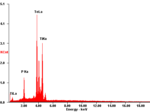
| Element | Wt% | At% |
|---|---|---|
| PK | 07.99 | 19.97 |
| TeL | 68.08 | 41.33 |
| TiK | 23.93 | 38.70 |
| Matrix | correction | ZAF |
| Band | Z2 invariants | ||
|---|---|---|---|
| 1 | (1;000) | ✓ | |
| 2 | (1;000) | ✓ | |
| 3 | (0;111) | ||
| 4 | (0;111) | ||
| 5 | (1;000) | ✓ | |
| 6 | trivial |
| Band | Z2 invariants | ||
|---|---|---|---|
| 1 | (1;000) | ✓ | |
| 2 | Trivial | ||
| 3 | (1;111) | ✓ | ✓ |
| 4 | (0;111) | ✓ | |
| 5 | (0;111) | ✓ | ✓ |
| 6 | (1;111) | ✓ | |
| 7 | Trivial | ||
| 8 | (0;111) | ✓ |
References
- [1] F. Philipp, P. Schmidt, M. Ruck, W. Schnelle, and A. Isaeva, J. Solid State Chem. , 2859 (2008).
- [2] J. S. Oh, H.-S. Yu, C.-J. Kang, S. Sinn, M. Han, Y. J. Chang, B.-G. Park, K. Lee, B. I. Min, S. W. Kim, H.-D. Kim, and T. W., Chem. Mater. , 7570 (2016).
- [3] G. Kresse and J. Furthmüller, Phys. Rev. B. 54, 11169–11186 (1996).
- [4] G. Kresse, and J. Furthmüller, Comput. Mater. Sci. 6, 15–50 (1996).
- [5] J. P. Perdew, K. Burke, and M. Ernzerhof, Phys. Rev. Lett. 77, 3865–3868 (1996).
- [6] G. Kresse, and D. Joubert, Phys. Rev. B 59, 1758–1775 (1999).
- [7] P. E. Blöchl, Phys. Rev. B 50, 17953–17979(1994).
- [8] M. M. Hosen, K. Dimitri, A. K. Nandy, A. Aperis, R. Sankar, G. Dhakal, P. Maldonado, F. Kabir, C. Sims, F. Chou et al., Nat. Commun. 9, 3002 (2018).