Defect characterization studies on neutron irradiated boron-doped silicon pad diodes and Low Gain Avalanche Detectors
Abstract
High-energy physics detectors, like Low Gain Avalanche Detectors (LGADs) that will be used as fast timing detectors in the High Luminosity LHC experiments, have to exhibit a significant radiation tolerance. Thereby the impact of radiation on the highly boron-doped gain layer that enables the internal charge multiplication, is of special interest, since due to the so-called Acceptor Removal Effect (ARE) a radiation-induced deactivation of active boron dopants takes place. In this paper we present defect-spectroscopy measurements (Deep-Level Transient Spectroscopy and Thermally Stimulated Current technique) on neutron irradiated p-type silicon pad diodes of different resistivity as well as LGADs irradiated at fluences up to ,\unitn_eq\per\centi□. Thereby we show that while for the silicon pad diodes irradiated with electrons, neutrons or protons the determination of defect electronic properties and defect introduction rates is straightforward, DLTS and TSC measurements on LGADs are strongly influenced by the impact of the gain layer. It is shown that the measurability of the capacitance of the gain layer shows a strong frequency and temperature dependence leading to a capacitance drop in DLTS and non-reliable measurement results. With TSC defects formed in the LGADs can be very nicely observed and compared to the defects formed in the silicon pad diodes. However the exact assignment of defects to the gain layer or bulk region remains challenging and the charge amplification effect of the LGADs impacts the exact determination of defect concentrations. Additionally, we will demonstrate that depending on the TSC measurement conditions defect induced residual internal electric fields are built up in the irradiated LGADs that are influencing the current signal of carriers emitted from the defect states.
keywords:
LGAD , defect spectroscopy , acceptor removal , DLTS , TSC , introduction rateOm
1 Introduction
Low Gain Avalanche Detectors (LGADs) are characterized by their high precision timing performance and are the selected technology for the Atlas High-Granularity Timing Detector (HGTD) as well as the CMS Endcap timing layer (ETL) [1, 2]. The operation of such sensors in the HL-LHC experiments requires a high radiation tolerance up to a 1 MeV neutron equivalent fluence of about \unit\per\centi□. For LGADs a radiation induced degradation in the device performance can be observed that correlates with changes in the effective doping concentration of the highly doped gain layer [3]. Normally the doping of such layer is up to cm-3 and enables charge multiplication due to impact ionization. The degradation becomes evident in a decrease in the signal gain with increasing particle fluence resulting in a disappearance of the multiplication effect at fluences of about cm [4].
The radiation-induced deactivation of boron in silicon (Si) is well-known as so-called Acceptor Removal Effect (ARE). Thereby, due to the interaction with high-energy particles, Si atoms are released from their lattice site and become Si interstitials (Si) which are very mobile, even at low temperatures, and interact via the Watkins replacement mechanism preferentially with boron and carbon atoms [5, 6] forming boron and carbon interstitials (B, C). These interstitials can further interact and create boron and carbon related defects like e.g. BB, BO, BC, CC or CO [7, 8]. Thereby the interstitial boron - interstitial oxygen complex (BO) is generally considered as main responsible defect for the boron deactivation. Although recent publications also state a BSi as possible defect structure to explain the ARE [9], in this publication we will follow the so far widely accepted assumption of a BO defect structure. Its creation is coupled with the deactivation of one negatively charged boron atom B and the formation of a donor type defect with an energy level in the upper part of the Si band gap (E - 0.25 eV). In this regard, the BO formation contributes with a factor of two to the changes of the space charge in the depletion region [8]. The formation of BO competes with the formation of CO which induces a hole trap at E + 0.36 eV and does not contribute to the ARE. This competition gives an explanation of the improved radiation hardness of carbonated LGAD gain layers [4]. In summary, the described defect kinetic model assumes that all interstitials created during the radiation interaction are forming either BO or CO defects [8]. This is very nicely reproduced in the experimentally observed dependency of BO introduction rates (IR = (defect concentration)/(fluence)) on the initial boron doping concentration for p-type silicon devices irradiated with fluences of up to 1015 \unitn_eq\per\centi□ [8]. However, it seems not be valid anymore for highly doped silicon, like the gain layers of LGADs, irradiated at fluences 1015 \unitn_eq\per\centi□ [8], since the generation rates that reflect the observed deactivation of boron extracted by changes of the macroscopic device properties are much higher as expected from the defect kinetic model [4, 8]. That raises the question if other defect structures might lead or contribute to the deactivation of acceptors in the highly doped LGAD gain layers. In order to trace back this question we present defect spectroscopy studies on silicon pad diodes and LGADs using the Deep-level Transient Spectroscopy (DLTS) and Thermally Stimulated Current (TSC) techniques.
2 Experimentals
The measurements were performed on LGADs and PIN diodes from CNM (Centro Nacional de Microelectrónica, Barcelona, Spain) and HPK (Hamamatsu Photonics, Japan). The LGAD structure is --- with a thin highly boron-doped multiplication layer () of around 2 \unit\micro (this layer is missing in the PIN diodes), a low doped active bulk region of about 50 \unit\micro () as well as the highly doped electrodes ( and ).
Irradiation was performed with reactor neutrons at the JSI in Ljubljana (Slovenia). The sample overview as well as the irradiation fluences are given in Table 1. The fluences given in this paper are normalized to 1 MeV neutron equivalent values () using the non-ionizing energy loss scaling (NIEL). The LGADs from CNM are from Run 11486 with an active area of 0.09 cm2 and a physical thickness of 351 \unit\micro. They consist of a low resistivity p-type support wafer and a 50 \unit\micro boron-doped active layer with a resistivity of about 5 kcm into which, during the sensor processing, an active p-type multiplication layer is implanted underneath the front electrode. The HPK LGADs have an active area of 0.0169 cm2 and consists of an a 300 \unit\micro support wafer, a 50 \unit\micro active p-type layer and an active highly-boron doped p-type multiplication layer. After irradiation all samples were annealed by default 10 min at 60\unit.
The defect spectroscopy measurements on the LGADs and PIN diodes are, among others, compared to similar studies performed on single boron-doped -- silicon pad diodes produced at CiS (Forschungsinstitut für Mikrosensorik GmbH, Erfurt, Germany) [10]. These diodes consist of an epitaxial grown boron-doped bulk layer of 50 \unit\micro that vary in resistivity from 10 cm to 1 kcm. The active area of those devices is cm2. They were irradiated with neutrons at JSI [11], with 24 GeV/c protons at IRRAD proton facility (CERN) [12], with 230 MeV protons at Boston General Hospital (USA) or with 200 MeV electrons at CLEAR (CERN) [13], and annealed afterwards for 10 min at 60\unit. As hardness factors for the calculation 0.62 was used for 23 GeV proton irradiation, 0.95 for 230 MeV proton irradiation and 0.082 for 200 MeV electron irradiation.
In order to investigate the macroscopic properties of the non-irradiated and irradiated diodes Capacitance-Voltage (-) measurements with different frequencies as well as Current-Voltage (-) measurements were performed. As defect spectroscopy methods Deep Level Transient Spectroscopy (DLTS) and Thermally Stimulated Current technique (TSC) were applied.
For DLTS a commercial system from PhysTech GmbH [14] was used. Thereby capacitance transients were analysed that were recorded after charge carrier injection at temperatures in the range from 20 K to 280 K, using three different time windows (20 ms, 200 ms and 2 s). The injection pulse was varied in time (t = 0.1 – 100 ms) and pulse voltage (UP). To inject only majority carriers a pulse voltage of UP = - 0.6 V was chosen, while for minority and majority carrier injection the pulse voltage was set to + 2 V. Before and after the injection pulse the device was put under reverse bias UR (typically UR = -10 V). The measurement frequency was 1 MHz.
TSC measurements were performed in the temperature range from 20 K to 220 K by using a Keithley electrometer and a Labview based DAQ. The typical measurement cycle for spectra presented in this paper consists of three steps:
(1) Cooling down: A reverse bias \unitUR_down is applied to the diode at high temperature ( 220 K). Afterwards the biased diode is subsequently cooled down to a certain filling temperature \unitT_fill (20 K to 90 K). This step assures the release of charges and the availability of unoccupied defect states.
(2) Filling step: At \unitT_fill a filling pulse UP (20 V) is applied to the sensor during a specific filling time (\unitt_fill = 60 s – 360 s). During this steps the defect states are occupied by majority and/or minority carriers.
(3) Heating up: the diode is put back under a reverse bias \unitUR_up and the temperature is raised with a constant heating rate of 11 K/min from \unitT_fill to 220 K. During this time the current signal induced by thermal emission of carriers from the defect levels is recorded. In case that \unitUR_down is equal to \unitUR_up the reverse bias is just named UR in this paper.
From the recorded TSC spectra the defect concentrations were determined by integration over the observed TSC peaks using the following equation [15]:
| (1) |
with : the elementary charge as well as : the area and : the thickness of the active region.
| (cm) | (V) | (V) | ||
| LGAD (HPK) | W36 S3-L15P5 | - | 50.8 (51.2) | |
| PIN (HPK) | W42 S4-L14P5 | 6.5 (7.2) | - | |
| LGAD (CNM) | r11486 W2-U23 | - | 27.0 (39.0) | |
| LGAD (CNM) | r11486 W3-A12 | - | 26.0 (30.5) | |
| PIN (CNM) | r11486 W2-X22 | 0.6 (1.8) | - | |
| LGAD (CNM) | r11486 W2-W22 | - | 14.0 (42.5) |
3 Results and Discussion
3.1 Electrical characterization and applicability of the DLTS method to LGADs
Before and after irradiation the LGADs and PIN diodes were electrically characterized by - and - measurements. The - measurements showed an increase in the leakage current, while the current related damage factor of A/cm, extracted from - curves at - 20∘C, agrees well with values given in the literature [15]. Furthermore, after irradiation a shift of the break down voltage to higher values was observed, that however decreases with decreasing the measurement temperature. - measurements on LGADs after irradiation have shown a decrease in the gain layer capacitance as well as a decrease of the depletion voltage of the gain layer () indicating the degradation of the gain layer due to the deactivation of active boron dopants. The of the investigated LGADs as well as the depletion voltage of the corresponding PIN diodes are given in Table 1.
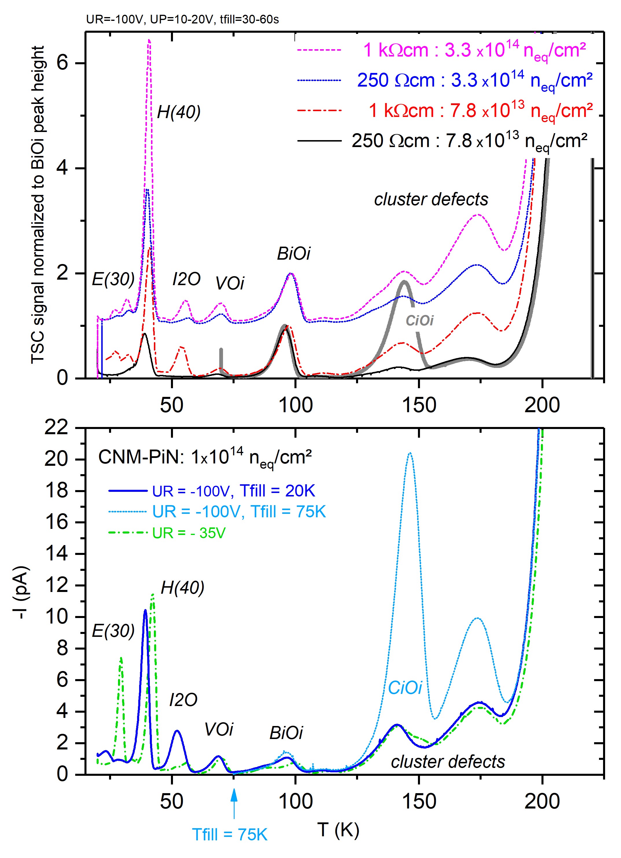
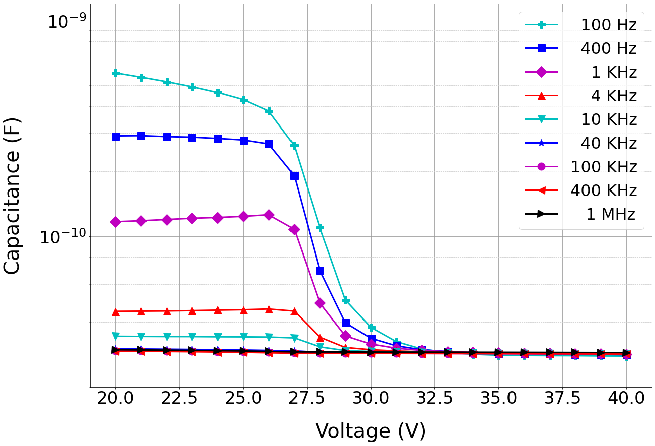
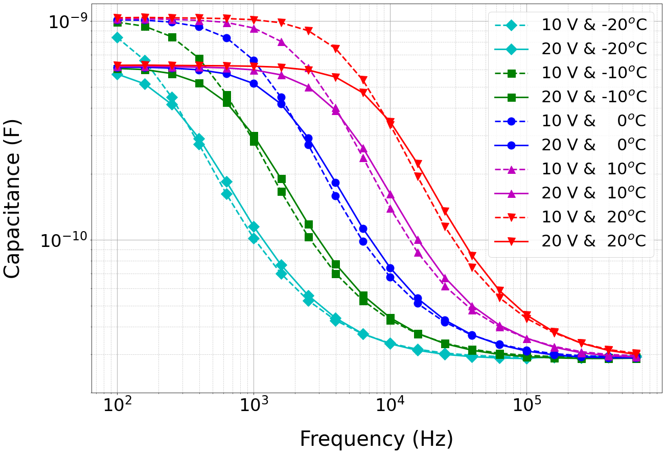
Figure 1 shows - measurements performed at different measurement frequencies on a CNM LGAD neutron irradiated with \unitn_eq\per\centi□. When using low measurement frequencies (standard: 10 kHz) while increasing the reverse bias it can be well distinguished between the depletion of the gain layer region up to the gain layer depletion voltage () and afterwards the depletion of LGAD bulk region. However for higher frequencies the measured capacitance of the gain layer region significantly drops. This effect becomes even more pronounced when decreasing the temperature as shown in Fig. 2. Here the capacitance values at a certain bias below are plotted against the measurement frequencies. The data are taken in the temperature range of - 20∘C to + 20∘C and demonstrate the increased capacitance drop with decreasing temperature.
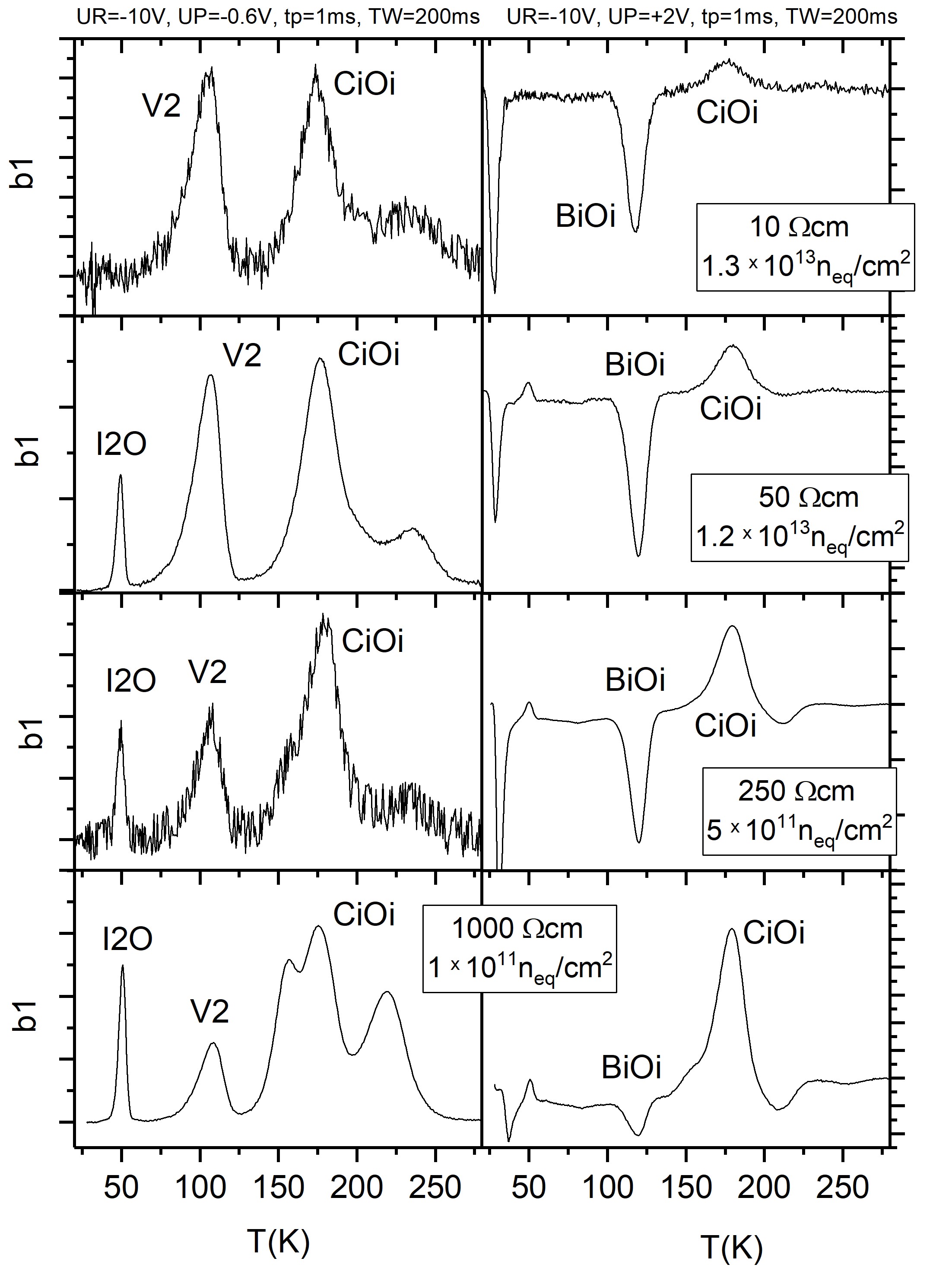
To perform DLTS measurements, temperatures down to 20 K were applied and a measurement frequency of 1 MHz is used. For the standard silicon pad diodes irradiated to adequate low fluence this allows the measurement of radiation induced defects very nicely as can be seen in Fig. 3. More details about the recorded spectra will be given below. On the other hand, DLTS measurements on LGADs
resulted in non-reliable spectra due to the strong capacitance drop at high frequencies. Also the highly irradiated PIN diodes could not be measured with DLTS since in this high resistivity diodes the net background doping level is small compared to the high defect concentrations induced by irradiation. That leads to non-exponential capacitance transients during the thermal emission process and prevents reliable DLTS results [16, 17].
The DLTS spectra in Fig. 3 are measured on EPI silicon pad diodes of resistivities from 10 cm to 1 kcm. The neutron fluences are and \unitn_eq\per\centi□ for the lower resistivity samples, and and \unitn_eq\per\centi□ for the diodes with higher resistivity.
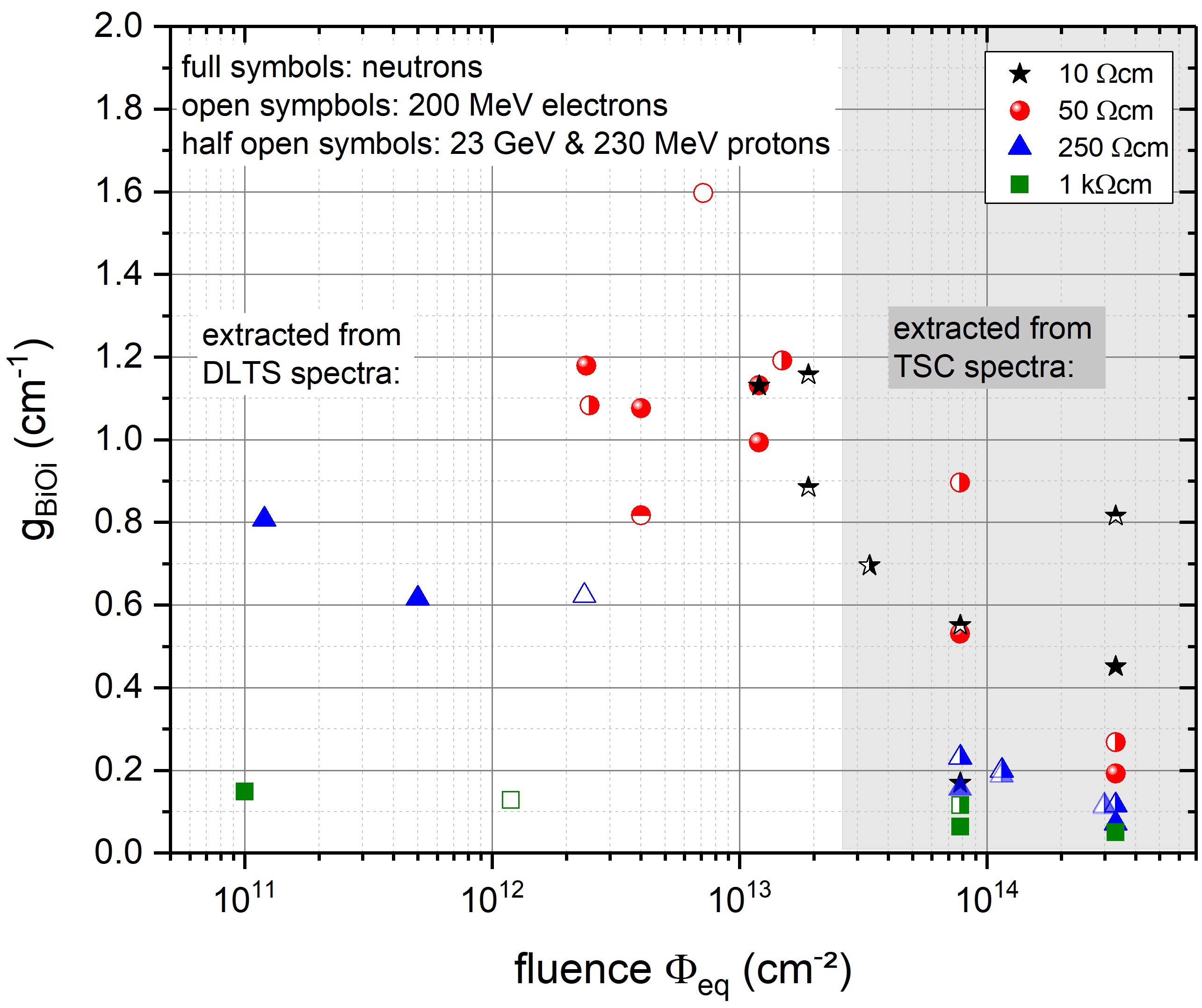
On the left-hand side, spectra obtained after injection of only majority carriers (holes) are shown while in the right-hand side the spectra after minority and majority carrier injection are plotted. As major electron trap the peak attributed to the BO defect can be very nicely seen. Analysis of the capacitance transients gave the defect concentrations from which we extracted the defect introduction rate for BO. They are plotted in Fig. 4 vs. particle fluence (white shaded area). The full symbols in this figure correspond to values taken from neutron irradiated diodes, while the open symbols and the half-open symbols are taken from comparable studies performed on 200 MeV electron irradiated diodes and 23 GeV as well as 230 MeV proton irradiated EPI silicon pad diodes, respectively.
As can be seen in Fig. 4, in the lower fluence range where DLTS is applicable the IR show rather a dependence on the device resistivity than on the fluence: for high resistivity material the IR are below 0.2 cm-1, medium resistivity samples show IR in the range of 0.6 to 0.8 cm-1, and for silicon pad diodes with low resistivities the values are above 0.8 cm-1 and in good agreement with previous experimental results on EPI silicon pad diodes [18, 19] as well as with the defect kinetic model described in the introduction [8]. Furthermore, in this fluence range no clear dependence of the IR on the particle type can be stated. However, a dependency of the IR on the particle type becomes visible at higher fluences, where the IR of proton irradiated sensors (half open symbols) are always higher than those of the neutron irradiated ones with the same resistivity (full symbols). This effect can be understood by a higher point defect formation ratio of protons compared to neutrons which preferentially create more cluster like defects [10]. A more detailed discussion about the IR rates obtained by TSC (grey shaded area in Fig.4) will be given in the next section.
3.2 TSC studies on silicon pad diodes and LGADs
Defect spectroscopy studies, including DLTS and TSC in combination with e.g. Electron Paramagnetic Resonance (EPR), Infra-Red absorption spectroscopy (IR) and detailed annealing studies, on a broad variety of irradiated silicon pad diodes have enabled the identification and assignment of a whole set of radiation induced defects in silicon [10, 20, 21, 22, 23, 24, 25, 26, 27, 28, 29, 30]. Figure 5 (top) shows TSC spectra of silicon pad diodes with 250 cm and 1 kcm resistivity, neutron irradiated with \unitn_eq\per\centi□ and \unitn_eq\per\centi□, respectively. The spectra are normalized to the BO peak height and those of the higher irradiated diodes are shifted on the y-axis to allow better visibility. Besides point defects like E(30), H(40), IO, VO, BO and CO, also multi-vacancy and cluster related defects (e.g. H(116), H(140), H(153)) [26, 25] at temperatures above 100 K can be distinguished. Since the free carrier capture cross section of the CO strongly depends on the filling temperature, it becomes visible in TSC only at higher \unitT_fill (see e.g. bold grey line in Fig. 5 with \unitT_fill = 70 K). In the temperature range of 96 K – 98 K we can identify the BO defect, that is assumed to be the main responsible defect for the radiation induced ARE.
By fitting the TSC peak area and applying Equation 1 we extracted the BO defect concentration and corresponding IR. The values are added in Fig. 4. All the IR for the BO that were obtained by TSC for the diodes irradiated with neutrons (or protons) at higher fluences are below the values extracted from DLTS at lower fluences. Thereby it should be mentioned that for the highly doped diodes (10 and 50 cm) an underestimation of the defect concentration has to be considered since those sensors were not able to fully deplete during the measurements. Therefore at least for those sensors the IR should be higher. The lower doped sensors (250 and 1 kcm) can be fully depleted and show the same trend of a reduced IR.
When comparing the types of defects created in the EPI silicon pad diodes with those created in the CNM PIN (see Fig. 5 (bottom)) irradiated to \unitn_eq\per\centi□ it is found that they are very comparable. When changing the filling temperature also in the PIN the CO peak becomes visible. The peak close to 100 K can be assigned to the BO with a concentration of about cm-3. To remember, the resistivity of the PIN diodes is below 5 kcm, resulting in an effective doping level of about cm-3. The BO IR would be around 0.02 cm-1. Here we should mention that the BO peak shows kind of a shoulder at the lower temperature side whose origin is not fully clear, yet, but could be connected to the so-called X-defect presented in the literature [19].
When changing the applied reverse bias (from -100 V to -35 V) the influence of the electrical field to the carrier emission becomes visible, and effects especially the TSC peaks at low temperatures, corresponding to defect levels near to the band gap edges (E). This so-called Poole-Frenkel effect is explained by an enhanced emission probability from Coulombic traps due to a field induced lowering of the emission barrier height for trapped charges [31, 32]. It leads in the TSC spectra to a peak shift to lower temperatures with increasing bias, and gives an explanation why for example the E(30) which is an electron trap with an energy level in the upper part of the band gap that shows a strong Poole-Frenkel effects [26], becomes visible only for low applied bias.
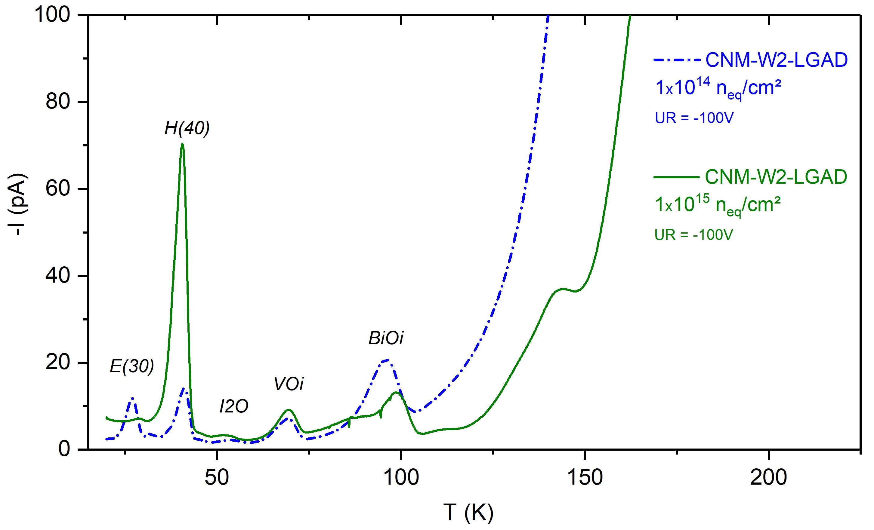
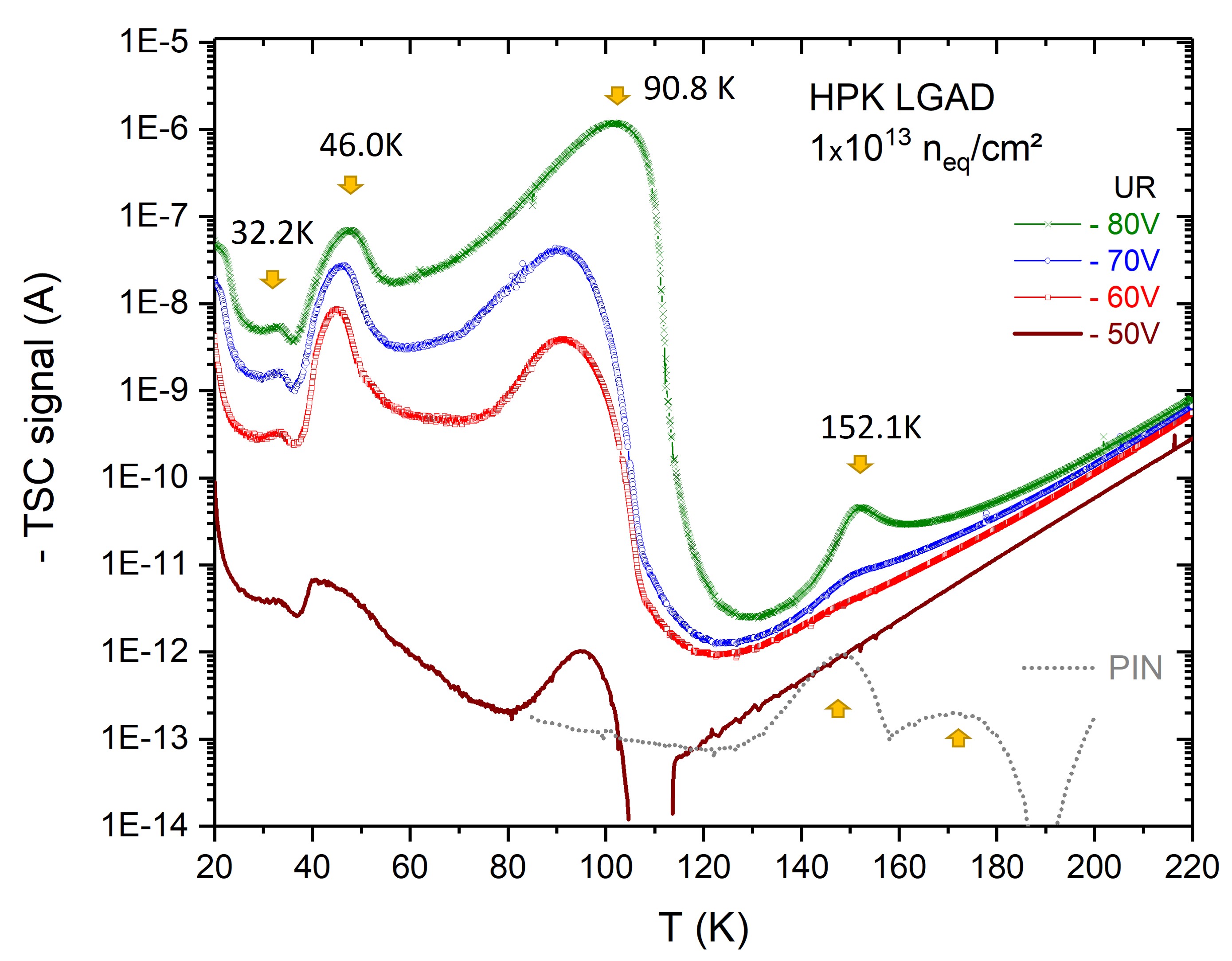
Figure 6 shows TSC spectra on CNM LGADs irradiated with different fluences (blue dash-dotted line: \unitn_eq\per\centi□ and green solid line: \unitn_eq\per\centi□). The reverse bias applied during the measurement was in both cases U = - 100 V, corresponding to full depletion of the device (gain layer and low doped bulk). From these spectra we could identify the same defect types as measured in the PIN diode, however the peak heights are higher in the LGAD spectra. So the BO concentration for the \unitn_eq\per\centi□ neutron irradiated LGAD is about cm-3 which gives an IR of about 0.2 cm-1. This IR is higher than for the PIN diodes but does not reach the values expected from the macroscopic sensor degradation given in the literature for highly doped LGAD gain layers [8]. Therefore, it is not very likely that this value reflects the deactivation of boron in the LGAD gain layer.
Furthermore, it is observed that the increase of the background leakage current, contributing to the TSC signal, starts at temperatures significantly lower compared to the PIN or silicon pad diodes. This increased current signal is an effect of the charge amplification in the gain layer of the LGADs. Therefore, in the higher irradiated LGAD, where the gain is expected to be more reduced due to the radiation induced acceptor removal, the impact of the background leakage current starts at higher temperatures than for the lower irradiated device.
The influence of the current amplification on the TSC signal becomes even more obvious when having a look on the measurements of \unitn_eq\per\centi□ irradiated HPK LGAD (see Fig. 7). When applying a reverse bias of U = - 80 V that corresponds to a full depletion of the device, the current signal induced by charge emission from defect states reach values of up to A. That would correspond to defect concentrations in the range of 1019 cm-3, being an effect of the charge amplification in the gain layer. Additionally it has to be taken into account, that for devices with multiplication layer the break-down voltage decreases with decreasing temperature [33]. For a non-irradiated HPK2-W36 LGAD it is around -50 V below 120 K compared to approximately -220 V at room temperature. In consequence it means that an exact determination of defect concentrations from the measured TSC spectra is not reliable unless the exact impact of the gain at the given temperatures on the emitted charges is known.
In a next step we checked if it is possible to distinguish between defects created in the gain layer and defects created in the low doped bulk of the devices by restricting the depletion region to the width of the gain layer region. To do so the reverse bias applied during the TSC measurements was reduced. This allows to deplete only a certain part of the device, like e.g. only the gain layer region. Thereby, the emitted charges during the heating up step are supposed to be released mainly from defects within those parts. For the lower irradiated HPK LGAD the changes in the TSC signal with decreasing reverse bias are shown in Fig. 7.
It can be seen that, up to the full depletion voltage of the gain layer (- 50 V), the defect related TSC current signal more and more decreases and is not anymore detectable for biases below the gain layer depletion voltage. In conclusion, for the low irradiated HPK LGAD it is not possible to give a trustable explanation whether the charges multiplicated at higher biases are coming from the bulk or gain layer region.
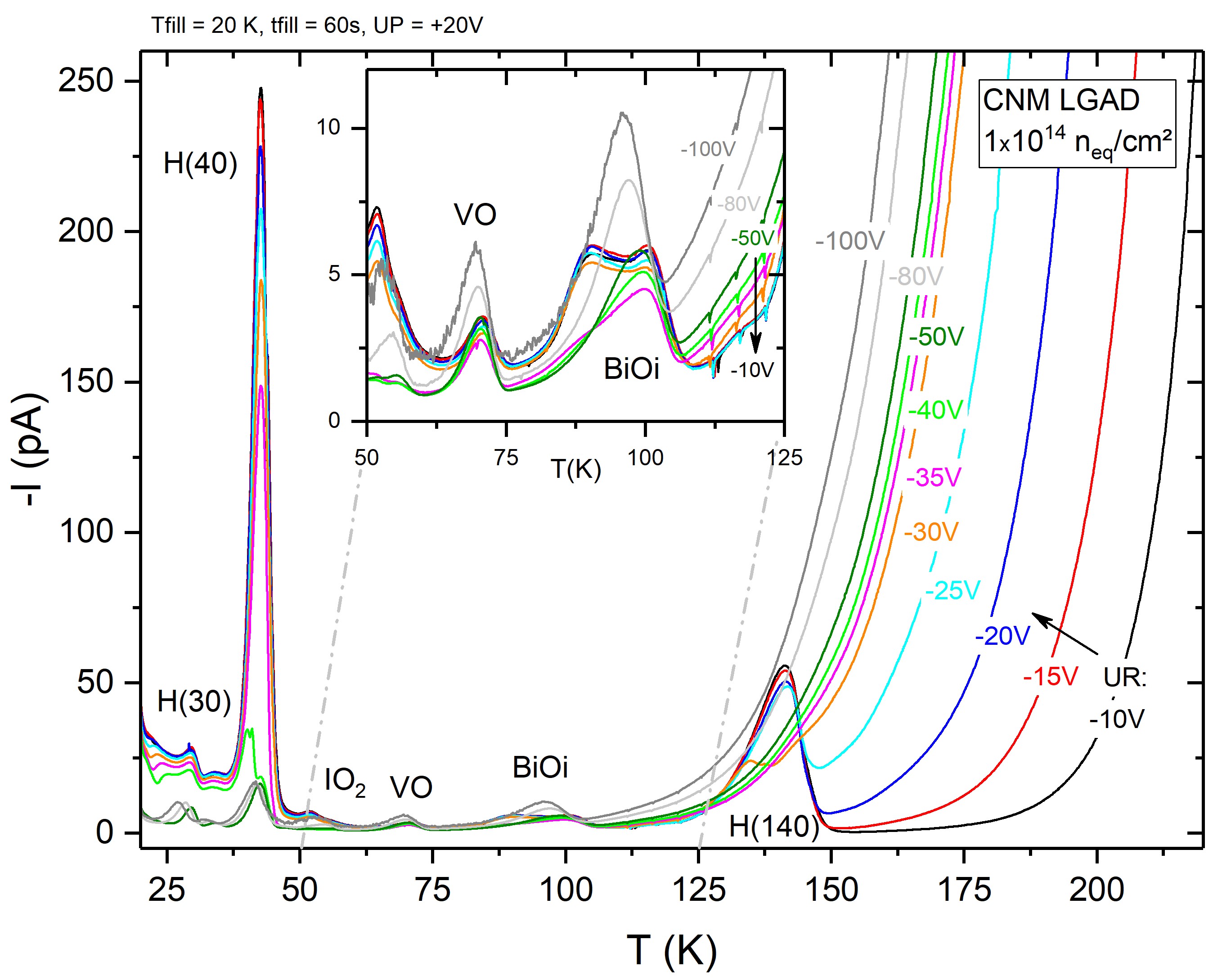
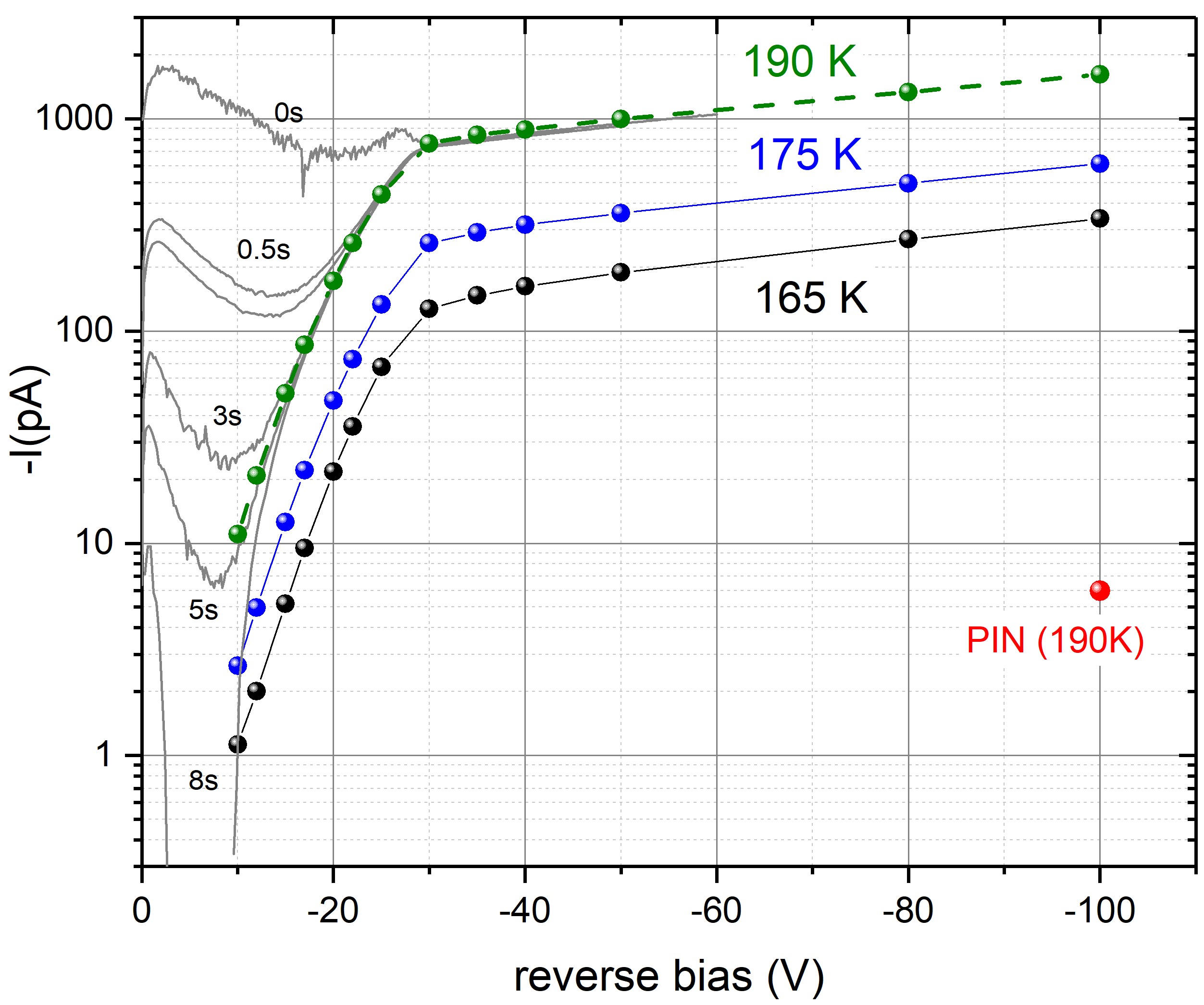
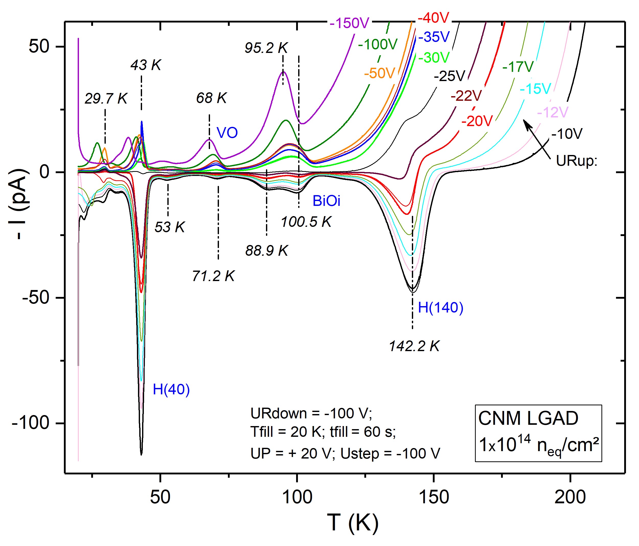
Comparable measurements performed on the higher irradiated CNM LGADs are illustrated in Fig. 8. First of all, one observes that with decreasing the bias voltage the background leakage current in the temperature region higher than 100 \unit decreases. The - dependence for three different temperatures (165 K, 175 K and 190 K), as extracted during TSC scan, is plotted in Fig. 9. The red dot corresponds to the TSC current signal at 190 K and -100 V bias for the corresponding PIN diode. Additionally added are also - measurements of the LGAD directly performed at 190 K from low to high bias voltage. They were recorded with different waiting times between two measurement points ( 10 s). The longer the waiting time, the better is the agreement of the - curve with the extracted values from TSC. The observed behaviour can be explained by taking into account the contribution of a time dependent displacement current at low bias. It even makes visible a sign inversion of the current signal for waiting times up to 8 s leading to a minimum current value of - 5.7 pA. For waiting times higher than 8 s no further changes in the measured - curves were observed. In summary, the - measurements reflect the behaviour observed during the TSC measurements and clearly demonstrates that at high voltages in the temperature range higher than 100 K the TSC signal is dominated by a high background leakage current. Therefore, when lowering the voltages during the TSC scan defect levels like the H(140) becomes visible (see Fig. 8). But also the TSC current intensities of the peaks at lower emission temperatures are influenced by the applied voltages. Especially the defect levels detected below 50 K strongly decrease in intensity when going from low to high voltages.
The inset in Fig. 8 shows a zoom of the TSC spectra between 50 K and 125 K. Normally the BO peak is expected to be measured at temperatures close to 100 K. While for low voltages this peak consists of two maxima at higher voltages they merge into one peak. A double peak structure in this temperature range was also observed for the low doped PIN diodes and might be induced by the appearance of the X-defect [19].
Additionally to the current sign inversion that was visible in the - measurements at low temperatures for low applied bias, also in TSC under certain measurement conditions an inversion in the TSC signal current was observed. This is illustrated in Fig. 10. The TSC spectra here were recorded after cooling down with -100 V reverse bias (TSC procedure: step 1), making a standard filling pulse (step 2) and after the filling pulse the reverse bias was set back to \unitU_step = -100 V (in the following called ”voltage step”) before applying the reverse bias \unitUR_up for ramping up the temperature (step 3). As seen in Fig. 10, if after the ”high voltage step” the reverse bias for ramping up is chosen to be smaller than the gain layer depletion voltage (- 10 V to - 25 V), the current induced by the emitted charges from defect states has a positive sign. With increasing the bias voltage up to the gain layer depletion voltage the detected emission current decreases and increases again with opposite sign for bias higher than the gain layer depletion voltage (- 30 V to - 150 V). The observed shifts in the defect peak maxima can by understood by the Poole-Frenkel effect. The same behaviour is also observed for the lower irradiated HPK LGADs (not shown) and appears independent of the bias voltage applied during the TSC cooling down step. The high voltage step after the filling leads to a full depletion of the device. Putting afterwards the bias back to lower values most probably creates internal electric fields that counteract to the external applied field, leading charge carriers moving opposite to the external applied field. From literature it is known, that changes in the TSC current sign can appear due to internal residual electrical fields that are induced by high defect concentrations [34, 35, 36].
4 Summary
In this paper we present defect spectroscopy studies (TSC and DLTS) on neutron irradiated silicon pad diodes as well as LGADs in order to understand the feasibility of using these methods to characterize defects in LGAD structures and find indications why the acceptor deactivation in the LGAD gain layer does not correlate with the defect kinetic model which is nicely applicable for the lower doped silicon pad diodes. We demonstrate a strong dependency of the gain layer capacitance on the measurement frequency and temperature, resulting in a capacitance drop during DLTS measurements that makes this method not reliable for defect characterization of LGADs. In contrast, with TSC the defects formed in the LGAD devices can be very nicely detected and compared to studies performed on silicon pad diodes. However, giving quantitative values for the defect concentrations, and therefore exact introduction rates for the boron deactivation, is challenging since the peak amplitudes are determined by the multiplication effect of the gain layer and makes it in addition difficult to clearly distinguish between defect signals coming from the low doped Si bulk or from the highly doped Si gain layer. In conclusion, based on the experimental results it can be stated that the defect spectroscopy methods we used are limited in characterizing defects in LGAD gain layers. In order to use the full potential of these methods it is therefore planned in a next step to process and characterize highly-irradiated silicon pad diodes with doping concentrations that mimic the gain layer of an LGAD.
CRediT authorship contribution statement
Anja Himmerlich: Conceptualization, Investigation, Formal analysis, Validation, Writing - Original Draft Nuria Castello-Mor: Software, Formal analysis Esteban Currás Rivera: Investigation, Formal analysis, Writing - Review & Editing Yana Gurimskaya: Investigation, Formal analysis, Validation, Writing - Review & Editing Vendula Maulerova-Subert: Software Michael Moll: Conceptualization, Writing - Review & Editing, Supervision, Project administration, Funding acquisition Ioana Pintilie: Validation, Conceptualization, Writing - Review & Editing, Project administration, Funding acquisition Eckhart Fretwurst: Conceptualization, Writing - Review & Editing, Project administration, Funding acquisition Chuan Liao: Validation, Writing - Review & Editing Jörn Schwandt: Conceptualization, Writing - Review & Editing, Project administration, Funding acquisition
Declaration of competing interests
The authors declare that they have no known competing financial interests or personal relationships that could have appeared to influence the work reported in this paper.
Acknowledgement
This work has been performed in the framework of the RD50 collaboration. I. Pintilie acknowledge the funding received through IFA-CERN-RO 08/2022 project. This project has received funding from the European Union’s Horizon 2020 Research and Innovation programme under GA no 101004761.
References
- [1] Technical proposal for a MIP timing detector in the CMS experiment phase 2 upgrade, Tech. Rep. CERN-LHCC-2017-027. LHCC-P-009, CERN, Geneva, https://cds.cern.ch/record/2296612 (Dec 2017).
- [2] Technical Proposal: A High-Granularity Timing Detector for the ATLAS Phase-II Upgrade, Tech. Rep. CERN-LHCC-2018-023. LHCC-P-012, CERN, Geneva, https://cds.cern.ch/record/2623663 (Jun 2018).
- [3] G. Kramberger, M. Baselga, V. Cindro, P. Fernández-Martínez, D. Flores, Z. Galloway, A. Gorisek, V. Greco, S. Hidalgo, V. Fadeyev, I. Mandić, M. Mikuz, D. Quirion, G. Pellegrini, H.-W. Sadrozinski, A. Studen, M. Zavrtanik, Radiation effects in Low Gain Avalanche Detectors after hadron irradiations, Journal of Instrumentation 10 (2015) P07006–P07006. doi:10.1088/1748-0221/10/07/P07006.
- [4] M. Ferrero, R. Arcidiacono, M. Barozzi, M. Boscardin, N. Cartiglia, G. D. Betta, Z. Galloway, M. Mandurrino, S. Mazza, G. Paternoster, F. Ficorella, L. Pancheri, H.-F. W. Sadrozinski, F. Siviero, V. Sola, A. Staiano, A. Seiden, M. Tornago, Y. Zhao, Radiation resistant LGAD design, Nuclear Inst. and Methods in Physics Research A 919 (2019) 16–26. doi:https://doi.org/10.1016/j.nima.2018.11.121.
- [5] G. D. Watkins, Intrinsic defects in silicon, Materials Science in Semiconductor Processing 3 (4) (2000) 227–235. doi:https://doi.org/10.1016/S1369-8001(00)00037-8.
- [6] R. Jones, A. Carvalho, J. Goss, P. Briddon, The self-interstitial in silicon and germanium, Materials Science and Engineering: B 159-160 (2009) 112–116, eMRS 2008 Spring Conference Symposium K: Advanced Silicon Materials Research for Electronic and Photovoltaic Applications. doi:https://doi.org/10.1016/j.mseb.2008.09.013.
- [7] L. C. Kimerling, M. Asom, J. Benton, P. Drevinsky, C. Caefer, Interstitial Defect Reactions in Silicon, in: Defects in Semiconductors 15, Vol. 38 of Materials Science Forum, Trans Tech Publications Ltd, 1989, pp. 141–150. doi:10.4028/www.scientific.net/MSF.38-41.141.
- [8] M. Moll, Acceptor removal - Displacement damage effects involving the shallow acceptor doping of p-type silicon devices, PoS Vertex2019 (2020) 027. 12 p. doi:10.22323/1.373.0027.
- [9] K. Lauer, K. Peh, S. Krischok, S. Reiß, E. Hiller, T. Ortlepp, Development of Low-Gain Avalanche Detectors in the frame of the acceptor removal phenomenon, Phys. Status Solidi (a) (2200177) (2020). doi:https://doi.org/10.1002/pssa.202200177.
- [10] Y. Gurimskaya, P. Dias de Almeida, M. Fernandez Garcia, I. Mateu Suau, M. Moll, E. Fretwurst, L. Makarenko, I. Pintilie, Radiation damage in p-type EPI silicon pad diodes irradiated with protons and neutrons, Nucl. Instrum. Meth. A 958 (2020) 162221. doi:10.1016/j.nima.2019.05.062.
- [11] https://www.ijs.si/ijsw/V001/JSI.
- [12] https://home.cern/science/accelerators/proton-synchrotron.
- [13] https://clear.cern/.
- [14] http://www.phystech.de.
- [15] M. Moll, Radiation damage in silicon particle detectors, PhD thesis, Uni Hamburg, 1999.
- [16] P. Blood, J. Orton, The electrical characterization of semiconductors: majority carriers and electron states, Academic Press, 1992.
- [17] D. V. Lang, Deep-level transient spectroscopy: A new methode to characterize traps in semiconductors, J. Appl. Phys. 45 (1974) 3032. doi:10.1063/1.1663719.
- [18] C. Besleaga, A. Kuncser, A. Nitescu, G. Kramberger, M. Moll, I. Pintilie, Bistability of the BiOi complex and its implications on evaluating the “acceptor removal” process in p-type silicon, Nuclear Instruments and Methods in Physics Research Section A: Accelerators, Spectrometers, Detectors and Associated Equipment 1017 (2021) 165809. doi:https://doi.org/10.1016/j.nima.2021.165809.
- [19] C. Liao, E. Fretwurst, E. Garutti, J. Schwandt, M. Moll, A. Himmerlich, Y. Gurimskaya, I. Pintilie, A. Nitescu, Z. Li, L. Makarenko, The boron-oxygen (BiOi) defect complex induced by irradiation with 23 GeV protons in p-type epitaxial silicon diodes, IEEE Trans. Nucl. Sci. 69 (3) (2022) 576–586. doi:10.1109/TNS.2022.3148030.
- [20] P. M. Mooney, L. J. Cheng, M. Süli, J. D. Gerson, J. W. Corbett, Defect energy levels in boron-doped silicon irradiated with 1 MeV electrons, Phys. Rev. B 15 (1977) 3836–3843. doi:10.1103/PhysRevB.15.3836.
- [21] J. R. Troxell, G. D. Watkins, Interstitial boron in silicon: A negative- system, Phys. Rev. B 22 (1980) 921–931. doi:10.1103/PhysRevB.22.921.
- [22] E. Fretwurst, C. Dehn, H. Feick, P. Heydarpoor, G. Lindström, M. Moll, C. Schütze, T. Schulz, Neutron induced defects in silicon detectors characterized by DLTS and TSC methods, Nuclear Instruments and Methods in Physics Research Section A: Accelerators, Spectrometers, Detectors and Associated Equipment 377 (2) (1996) 258–264. doi:https://doi.org/10.1016/0168-9002(95)01405-5.
- [23] N. Zangenberg, J.-J. Goubet, A. Nylandsted Larsen, On-line DLTS investigations of the mono- and di-vacancy in p-type silicon after low temperature electron irradiation, Nuclear Instruments and Methods in Physics Research Section B: Beam Interactions with Materials and Atoms 186 (1) (2002) 71–77. doi:https://doi.org/10.1016/S0168-583X(01)00876-X.
- [24] I. Pintilie, M. Buda, E. Fretwurst, G. Lindström, J. Stahl, Stable radiation-induced donor generation and its influence on the radiation tolerance of silicon diodes, Nuclear Instruments and Methods in Physics Research Section A: Accelerators, Spectrometers, Detectors and Associated Equipment 556 (1) (2006) 197–208. doi:https://doi.org/10.1016/j.nima.2005.10.013.
- [25] I. Pintilie, E. Fretwurst, G. Lindström, Cluster related hole traps with enhanced-field-emission - the source for long term annealing in hadron irradiated Si diodes, Appl. Phys. Lett. 92 (2) (2008) 024101. doi:10.1063/1.2832646.
- [26] I. Pintilie, G. Lindstroem, A. Junkes, E. Fretwurst, Radiation-induced point- and cluster-related defects with strong impact on damage properties of silicon detectors, Nuclear Instruments and Methods in Physics Research Section A: Accelerators, Spectrometers, Detectors and Associated Equipment 611 (1) (2009) 52–68. doi:https://doi.org/10.1016/j.nima.2009.09.065.
- [27] V. P. Markevich, A. R. Peaker, B. Hamilton, S. B. Lastovskii, L. I. Murin, J. Coutinho, V. J. B. Torres, L. Dobaczewski, B. G. Svensson, Structure and electronic properties of trivacancy and trivacancy-oxygen complexes in silicon, physica status solidi (a) 208 (3) (2011) 568–571. doi:https://doi.org/10.1002/pssa.201000265.
- [28] R. Radu, E. Fretwurst, R. Klanner, G. Lindstroem, I. Pintilie, Radiation damage in n-type silicon diodes after electron irradiation with energies between 1.5 MeV and 15 MeV, Nuclear Instruments and Methods in Physics Research Section A: Accelerators, Spectrometers, Detectors and Associated Equipment 730 (2013) 84–90, proceedings of the 9th International Conference on Radiation Effects on Semiconductor Materials Detectors and Devices. doi:https://doi.org/10.1016/j.nima.2013.04.080.
- [29] R. Radu, I. Pintilie, L. C. Nistor, E. Fretwurst, G. Lindstroem, L. F. Makarenko, Investigation of point and extended defects in electron irradiated silicon — Dependence on the particle energy, Journal of Applied Physics 117 (16) (2015) 164503. doi:10.1063/1.4918924.
- [30] E. M. Donegani, E. Fretwurst, E. Garutti, R. Klanner, G. Lindstroem, I. Pintilie, R. Radu, J. Schwandt, Study of point- and cluster-defects in radiation-damaged silicon, Nuclear Instruments and Methods in Physics Research Section A: Accelerators, Spectrometers, Detectors and Associated Equipment 898 (2018) 15–23. doi:https://doi.org/10.1016/j.nima.2018.04.051.
- [31] J. Frenkel, On pre-breakdown phenomena in insulators and electronic semi-conductors, Phys. Rev. 54 (1938) 647–648. doi:10.1103/PhysRev.54.647.
- [32] J. L. Hartke, The Three-Dimensional Poole-Frenkel Effect, J. Appl. Phys. 39 (1968) 4871–4873. doi:10.1063/1.1655871.
- [33] D. J. Massey, J. P. R. David, G. J. Rees, Temperature dependence of impact ionization in submicrometer silicon devices, IEEE Transaction on Electron Devices 53 (9) (2006) 2328. doi:10.1109/TED.2006.881010.
- [34] I. Pintilie, C. Tivarus, T. Botila, D. Petre, L. Pintilie, Experimental evidence of deep electron and hole trapping levels in high fluence proton irradiated p–n si junctions using optical charging spectroscopy, Nuclear Instruments and Methods in Physics Research Section A: Accelerators, Spectrometers, Detectors and Associated Equipment 439 (2) (2000) 221–227. doi:https://doi.org/10.1016/S0168-9002(99)00887-6.
- [35] M. Bruzzi, R. Mori, M. Scaringella, D. Menichelli, Optimization of the priming procedure for thermally stimulated current with heavily irradiated silicon detectors, PoS RD09 (2009) 018, https://pos.sissa.it/098/018/pdf.
- [36] D. Menichelli, R. Mori, M. Scaringella, M. Bruzzi, Zero-bias thermally stimulated currents (ZB-TSC) spectroscopy of deep traps in irradiated silicon particle detectors, Nuclear Instruments and Methods in Physics Research Section A: Accelerators, Spectrometers, Detectors and Associated Equipment 612 (3) (2010) 530–533. doi:https://doi.org/10.1016/j.nima.2009.08.049.