Electrical and thermal transport through NIS junction
Abstract
We investigate the electrical and thermal transport properties of the based normal metal-insulator-superconductor (NIS) junction using Blonder-Tinkham-Klapwijk (BTK) theory. We show that the tunneling conductance of the NIS junction is an oscillatory function of the effective barrier potential () of the insulating region upto a thin barrier limit. The periodicity and the amplitudes of the oscillations largely depend on the values of and the gate voltage of the superconducting region, namely, . Further, the periodicity of the oscillation changes from to as we increase . To assess the thermoelectric performance of such a junction, we have computed the Seebeck coefficient, the thermoelectric figure of merit, maximum power output, efficiency at the maximum output power of the system, and the thermoelectric cooling of the NIS junction as a self-cooling device. Our results on the thermoelectric cooling indicate practical realizability and usefulness for using our system as efficient cooling detectors, sensors, etc., and hence could be crucial to the experimental success of the thermoelectric applications of such junction devices. Furthermore, for an lattice, whose limiting cases denote a graphene or a dice lattice, it is interesting to ascertain which one is more suitable as a thermoelectric device and the answer seems to depend on the . We observe that for an lattice corresponding to , graphene () is more feasible for constructing a thermoelectric device, whereas for , the dice lattice () has a larger utility.
I Introduction
After the remarkable discovery of being able to extract graphene monolayer [1, 2], the realization of a perfect two dimensional (2D) material could be achieved. On a more fundamental note, Dirac physics in realistic systems became one of the most explored topics in the field of condensed matter physics. Graphene, a two dimensional single layer of honeycomb lattice (HCL) formed of carbon (C) atoms, manifests a low-energy spectrum which is linear in momentum and obeys a (pseudospin) Dirac-Weyl equation. The conduction band meets the valence band at six corner points of the hexagonal Brillouin zone (BZ), known as the Dirac points. Due to the presence of the Dirac-like energy spectrum of quasiparticles, a number of fascinating physical phenomena, such as anomalous quantum Hall effect [3, 4], chiral tunneling [5, 6], Klein paradox [5, 7] have emerged as distinctive properties of graphene. Furthermore, it has generated tremendous interest in different fields, such as electronics [8], optoelectronics [9, 10], and spintronics [11, 12, 13] in the recent years. Moreover, it has been predicted that a graphene normal metal-superconductor (NS) and a normal metal-insulator-superconductor (NIS) junction can exhibit specular Andreev reflection in addition to the usual retro-reflection. The conductance characteristics of the junction systems and their utilities for heat transport are of prime importance in this work.
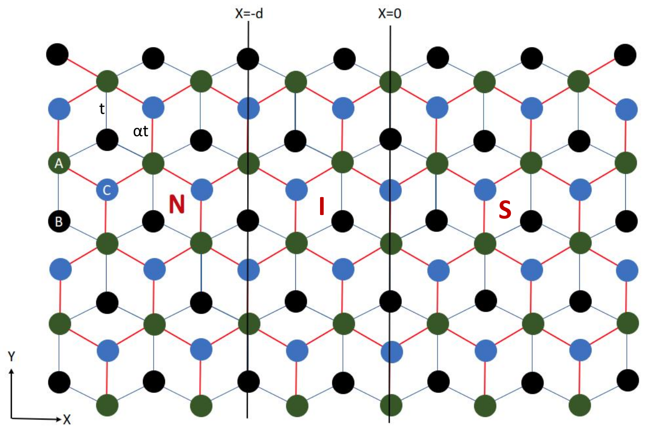
An interesting variant of the honeycomb structure, or in other words, graphene, exists which goes by the name -lattice [14], where the quasiparticles obey the Dirac-Weyl equation with pseudospin . This lattice is a special honeycomb like structure with an additional atom sitting at the corner of each hexagon. A unit cell of the lattice comprises of three non-equivalent lattice sites, where two sites, generally known as the sites, are located at the corner points of HCL. The other lattice site, called as the site, is situated at the center of HCL. The sites are connected to the three nearest neighbors (NNs), while the hub site is connected to six NNs. The hopping strength between the site and one of the sites is proportional to a parameter , as shown in Fig.1 (upper panel). The strength of may be considered as a tunable parameter and at the extremities of the range [0:1] lie graphene and a dice lattice respectively [15, 16, 17, 18, 19, 20, 21, 22]. The low-energy excitations of the lattice near the Dirac points consist of three branches. Two of them linearly disperse with momentum, generally known as the conic bands, while the third, being non-dispersive energy band is termed as a flat band. All the six band-touching points (the so called Dirac points) in the first BZ lie on the flat band.
A dice lattice can be realized by growing trilayers of cubic lattices (e.g., SrTiO3/SrIrO3/SrTiO3) in the (111) direction [23]. Further, in the context of cold atom, a suitable arrangement of three counterpropagating pairs of laser beams [19] can produce an optical dice lattice. Moreover, the Hamiltonian of a Hg1-xCdxTe quantum well at a certain critical doping can also be mapped onto the model in the intermediate regime (between dice and graphene), corresponding to a value of [24] where the band structure comprises of linearly dispersing conduction and valence bands, plus a flat band.
A good number of physical quantities, such as the Berry-phase-dependent direct current (DC) Hall conductivity [25], dynamical optical conductivity [25], magneto-optical conductivity, the Hofstadter butterfly [26, 27, 28], Berry-phase-modulated valley-polarized magnetoconductivity [29], the photoinduced valley and electron-hole symmetry breaking [30] in the lattice have been studied recently. Further, other properties, such as the conductivity [31, 32], super-Klein tunneling [33, 34, 35, 36], gap generation and flat band catalysis [37, 38], non-linear optical response [39], topological phase transition[40, 41, 42, 43, 44], electronic and optical properties under radiation [45, 46], flat-band induced diverging DC conductivity [22], and the thermoelectric performance of a nanoribbon [47] of lattice have also been explored. Moreover, nontrivial topology[48, 49, 50, 51, 52, 53], the diamagnetic[54] (at ) to paramagnetic[15, 16] (at ) transition in the orbital magnetic responses of the lattice have also been reported.
Recently, quantum transport studies through such junction systems have gained much more impetus in the field of developing nano-scale devices [55]. The junction devices have compelling applications in the fields of thermoelectric, thermometric, solid-state cooling, etc. Previously, numerous studies have been performed [57, 56, 58, 59, 60, 61, 62, 63], where the junction devices are found to be useful in a wide range of applications in low-temperature thermometry and electronic cooling [64, 65, 66]. The recent advancement in the field of thermoelectric physics in small-scale junction devices have provided new directions for manufacturing self-cooling devices, thermopower devices, etc.
Motivated by the above prospects of junction system at the nanoscale, we perform an extensive study of the electrical and the thermal transport in based NIS junction system using the modified Blonder-Tinkham-Klapwijk (BTK) theory that adequately captures the low-energy transmission characteristics. In particular, we compute the differential conductance of the NIS junction as a function of the effective barrier potential (defined in the next section) for different values of the parameter . Further, we calculate the Seebeck coefficient, charge conductance, thermal conductance, figure of merit, maximum power, efficiency at maximum power, thermal current of such based NIS junction, and explore an interplay between (to interpolate between graphene and a dice lattice) and the effective barrier potential on their performance of these junction systems.
This paper is organized as follows. In Sec. II, we present the basic information regarding the junction (Sec. II.1) and the definitions of different thermoelectric coefficients (Sec. II.2, Sec. II.3, and Sec. II.4) that we shall be studying here. Section III includes details of the numerical results and their corresponding discussions. Finally, we conclude and summarize our main results in Sec. IV.
II Model and Formalism
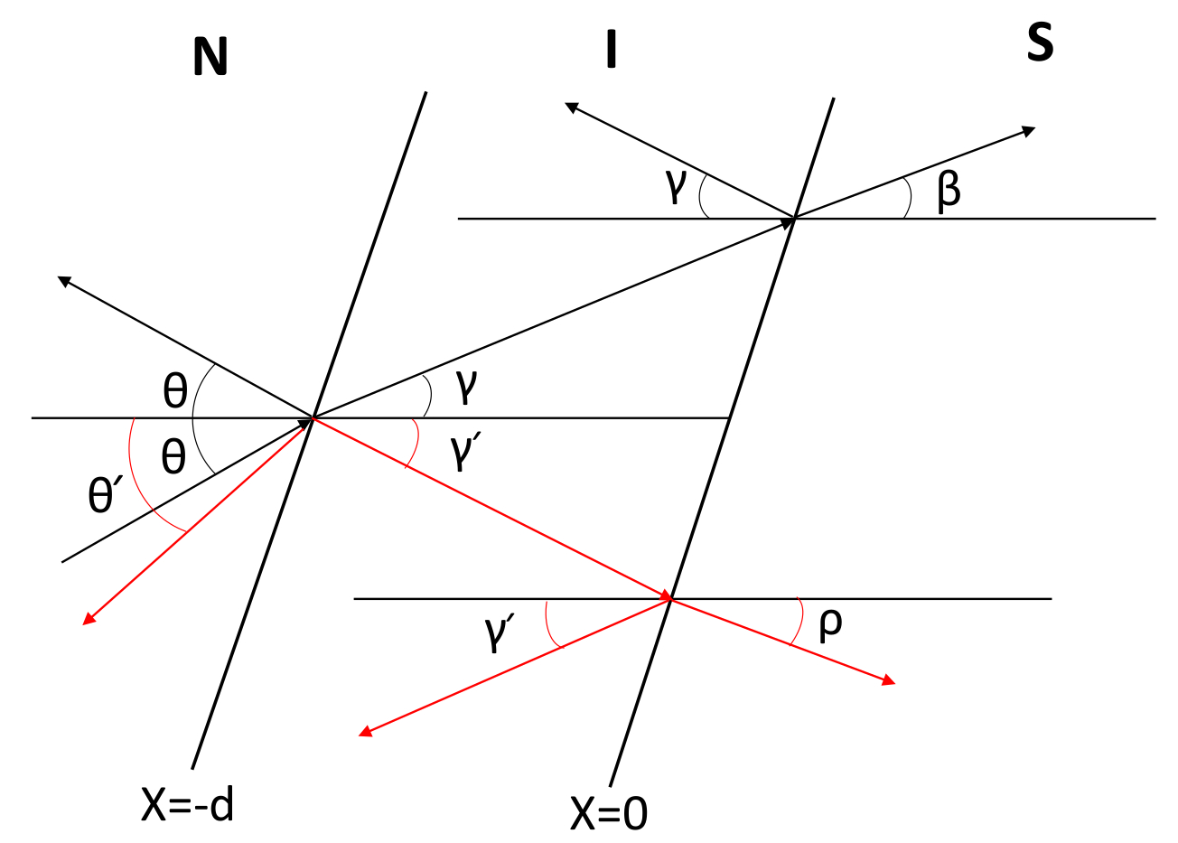
This section initially presents all the essential information of our junction system, where the electron transport lies in the quasi-ballistic regime. In Fig.1 (lower panel), we have shown the schematic illustration of all the reflection and the transmission processes of the quasiparticles at different regions of the NIS junction system. The later part includes the general description of thermoelectric coefficient, charge conductance, thermal conductance, figure of merit (FM), maximum power, efficiency at maximum power, and thermal current along with thermoelectric cooling for any junction system.
II.1 Information of the junction system
We consider an NIS junction made of sheet, occupying the plane (see Fig.1(upper panel)). The left lead, i.e., the normal region (N) extends from to for all . The middle region, i.e., the insulating regime () is characterized by a barrier potential , extending from to . The right superconducting lead (S) occupies the region . The local barrier in the insulating regime can be implemented either using by an external electric field or a local chemical doping [67, 68, 69, 70]. The superconductivity in the right lead can be induced via a proximity effect [71, 72]. It is to be noted that the barrier region has sharp edges on both sides, thus the insulating regime has to satisfy the condition: , where is the Fermi wave vector for an lattice. The NIS junction of our consideration can be described by the Dirac-Bogoliubovde Gennes (DBdG) equation [71, 73, 74]
| (1) |
where is the Fermi energy of system, denotes the macroscopic phase in the superconducting regime, is the time-reversal operator with being the Pauli matrix, C being the operator of complex conjugation and . Further, denotes the excited energy of electron and hole, and are the electron (electron-like) and hole (hole-like) wave functions in the normal (superconducting) regime, respectively and denotes a unit matrix. The zero temperature superconducting gap, is induced in the lattice by addressing a conventional -wave superconductor. The Hamiltonian in lattice can be written as,
| (2) |
where with,
| (3) |
and
| (4) |
Here, is the Fermi velocity, the label denote the and valleys, respectively. The angle is related to the strength of coupling parameter via . The potential gives rise to the relative shift in Fermi energies for normal, insulating, and superconducting regimes of sheet, where is modeled as with being the Heaviside step function. Now, we introduce a dimensionless barrier strength via [73],
| (5) |
which is going to play a pivotal role in all our subsequent discussions. We consider a thin barrier, such that with and , remains finite. For a NS (normal-superconductor) junction vanishes. The gate potential can mimic the Fermi surface mismatch between the normal and superconducting regimes. It is to be noted that the mean-field conditions for superconducting regime are satisfied as long as . Thus, in principle, for large one can have regimes where .
Because of the time-reversal symmetry of the lattice (), Eq.(1) can be decoupled into two sets of six equations with the form,
| (6) |
We consider only because of the valley degeneracy. The energy dispersion can be written as , with in both the normal and superconducting regions. For a given and , the four eigenstates in the normal region (, ) are obtained as
| (7) |
and
| (8) |
The state () denotes the electron (hole) moving along direction (i.e., towards the normal metal-insulator (NI) junction), while () denotes the electron (hole) moving along direction (away from the NI junction). Further, the angles and denote the incident angle of an electron and the reflected angle of the corresponding hole, respectively. The wave vector () represents the longitudinal wave vector of the electron (hole).
The wave functions in the superconducting region () are obtained as,
| (9) |
with , and for , for .
Similarly, in the intervening region (), one can obtain,
| (10) |
and
| (11) |
with and being the corresponding wave vectors. The eigenstate () denotes the electron (hole) moving along direction (i.e., towards the insulator-superconductor (IS) junction), where () denotes the electron (hole) moving along the direction (i.e., away from the IS junction). Thus, the wave functions in the normal, insulating and superconducting regimes can be written as,
| (12) | |||||
where and are the amplitudes of normal and Andreev reflections, respectively, in the normal regime; and are the amplitudes of the incoming and reflected electrons in the insulating regime, and denote the amplitudes of incoming and reflected holes in the insulating region. Further, and correspond to coefficients of transmission to the superconducting regime as electron-like and hole-like quasiparticles, respectively.
The wave functions must satisfy the following boundary conditions:
| (13) |
Using the boundary conditions, one can obtain the normal reflection coefficient and Andreev reflection coefficient . With some straightforward, although cumbersome algebra, we find that in the limit of a thin barrier, the expressions for and depend on the dimensionless barrier strength as,
| (14) |
and
| (15) |
where,
| (16) | |||||
and
| (17) | |||||
Using the BTK formalism, the differential conductance at zero temperature is given by,
| (19) |
with , , and . Considering the two-fold spin and valley degeneracies, is the ballistic conductance with being the transverse modes in the lattice with a total width, .
II.2 Seebeck coefficient
Here, we present the theory to calculate the Seebeck coefficient. A temperature difference between two dissimilar materials produces a voltage difference, and this phenomenon is known as the Seebeck effect. For our system, the normal and the superconducting leads are subjected to a temperature difference and there will be a voltage difference (say) between the two leads. The thermopower or the Seebeck coefficient is defined as the voltage induced per unit temperature difference in an open circuit condition. Hence we can write
| (20) |
We consider the left and right electrodes as independent temperature reservoirs, where the left and right electrodes are kept at temperature and , respectively. The populations of electrons in the left and right leads are described by the Fermi-Dirac distribution functions, namely, and , respectively, where at zero external bias.
In an open circuit condition, let us now consider an extra infinitesimal current induced by an additional voltage and the temperature difference across the junction. The currents induced by and are given by, and . Suppose the induced current cannot flow in an open circuit condition, where should counter-balances . Hence, we can write,
| (21) |
Performing the first order expansion of Fermi-Dirac distribution function in and with energy shifted by Fermi energy, one can obtain the expression of Seebeck coefficient,
| (22) |
where , and is the Fermi-Dirac distribution function.
II.3 Maximum power, efficiency at maximum power, and figure of merit
The most challenging part to fabricate a thermoelectric device is to find the optimal conditions which ensure the operation of the device with maximum power output at the best possible efficiency. We are also looking for a condition to derive maximum power output from our NIS junction system, where the maximum power is given by,
| (23) |
with [77]. Now, for optimal operation of the thermoelectric device, its function with the highest possible efficiency is also have to be considered. The efficiency () of the thermoelectric system is taken to be the ratio of the power to the thermal current or in other words the efficiency of a device is defined as the ratio of useful output power to the input power. Since our main focus is to look into the operation of the NIS junction system at the maximum power, we, therefore, concentrate upon the efficiency calculated at the maximum power which is given by [77, 78],
| (24) |
where is the Carnot efficiency. The efficiency of the system depends upon a quantity called the figure of merit ZT, which is defined as,
| (25) |
where is the Seebeck coefficient, is the charge conductance, is the thermal conductance, and is the absolute temperature. can be calculated from the relation
| (26) |
where is the normal state resistance, defined as (2 is the spin degeneracy factor, is the density of states at the Fermi level, is the Fermi velocity, and is the area of contact). The thermal conductance, can be calculated from the relationship , where is the thermal current flowing from the normal lead to the superconducting lead. In the next subsection, we present how the thermal current and the thermal conductance can be calculated.
II.4 Thermoelectric cooling and thermal conductance
The flow of electrons can also transport thermal energy through the junction, which is responsible for the thermal current. The thermal current is defined as the rate at which the thermal energy flows from the left lead to the right lead, where the left electrode serves as the cold reservoir and the right one serves as the hot reservoir. An external bias voltage drives the electrons to flow from normal to superconducting lead. Thus, the electron removes the heat energy from the normal lead and transfers it to the superconducting lead which further makes the cold reservoir (normal) cool. The energy conservation allows us to write,
| (27) |
Using the analogy between electronic charge current and electronic thermal current, one can write the outbound energy flow rate from normal lead to superconducting lead as,
| (28) |
Similarly, the reverse, that is the rate at which the superconducting lead receives the thermal energy, is written as
| (29) |
where the energies are shifted by Fermi energy and .
The thermal conductance can be obtained from the temperature derivative of , that is, . This junction system can be regarded as the electronic cooling device only when , which indicates that it is competent to remove the heat from cold reservoir and hence making it cooler. The thermal conductance, is given by the form,
| (30) |
III Results and Discussions
Here, we present numerical results of zero temperature differential conductance and different thermoelectric properties of the based NIS junction. Putting things in perspective, we have considered some reasonable values of at 1meV, and (in the subsequent discussions, Fermi energy of the normal metal regime will consider as ). For thermoelectric studies, the temperature of the cold lead is kept at , whereas the hot lead is kept at with . We have varied the temperature in such a range so that the superconductivity is not destroyed. The dimension of the system is in the range of a few nanometer.
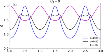
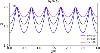
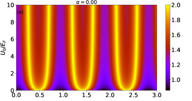
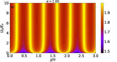
A. Differential Conductance (at T = 0 K): The differential conductance (at zero temperature) as a function of effective barrier potential for different values of is shown in Fig.2. We consider two cases: , , the Fermi energy of the superconducting region is taken as, , and i.e. the Fermi energy of superconducting region is much greater than the Fermi energy of the normal region. We have chosen so that the leakage of Cooper pairs from the S to N regions can be safely neglected [71, 75, 76].
Fig.2 shows Fabry-Perot like oscillation in the conductance pattern for both the cases indicating electron interferences. For case , where the Fermi surfaces of the normal metal and the superconductor are aligned () and , the oscillations are exactly in opposite phase for and . For , the periodic oscillations show maxima at , where for , the periodic oscillations show maxima at (see Fig.2a) . For a intermediate case, i.e., for any values of lying between and , a hump-like feature is obtained in the oscillations. As we know, for a Fabry-Perot interferometer the maxima and the minima depend on the path difference of the light passing through it, similarly here also, as we go from (graphene) to (dice lattice), the electrons travel an extra path which comes out with exactly opposite in phases. Further, it is noticeable that the amplitudes of oscillations are different for different values of . As we know, for a Fabry-Perot oscillator the amplitudes depend upon the reflectivities of the first (analogous to NI interface of our system) and second mirror (analogous to IS interface of our system) of the resonator. Similarly, for the lattice, the amplitudes of oscillation decrease as we go from to , indicating an increase in normal reflection coefficient (), while a decrease in the Andreev reflection coefficient (). Now, we consider case , where we increase the value of . The oscillations tend to occur in the same phase for all values of , as shown in Fig.2b and the maxima occur at . Here, the periodicity decreases to for all values of . For , the oscillations are exactly in the same phase, but their amplitudes are different.
Fig.3 shows a color plot of the differential conductance, () as a function of the effective barrier potential and the gate voltage in the superconducting region . It is clear that for low values of , the maxima of the conductance appear at different values of for both (Fig.3a) and (Fig.3b) cases. But for greater values of , the maxima appears at the same value of .
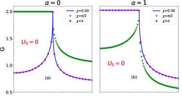
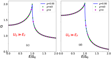
Further, in Fig.4, we show the tunneling conductance as a function of incident energy () for different values of with and . It is clearly visible that for (graphene) and (Fig.4a), the tunneling conductance at the gap edge reaches a value close to when (for any integer ), the conductance repeats for . While for (dice) and (Fig.4b), the tunneling conductance at the gap edge reaches a value close to when with a periodicity . However, with for both the graphene (Fig.4c) and the dice (Fig.4d) cases, the maximum conductance occurs at with a periodicity .
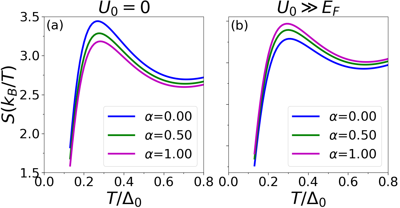
B. Seebeck Coefficient: The variation of the Seebeck coefficient as a function of temperature (in units of superconducting gap, ) is shown in the Fig.5a, and Fig.5b. Here also, we consider two cases: and with . Further, we consider a particular value of , where the charge conductance records the maximum value. We represent the Seebeck coefficient in unit of (). For both the cases (see Fig.5a), and (see Fig.5b), the Seebeck coefficient shows maximum values at . It is understood that the Seebeck coefficient increases initially with temperature and after attaining a certain value it decreases for all values of .
Further, we observe that the maximum of the Seebeck coefficient decreases with the increasing strength of for (Fig.5a), while for , the reverse trend is obtained in Fig.5b.
C. Charge Conductance:
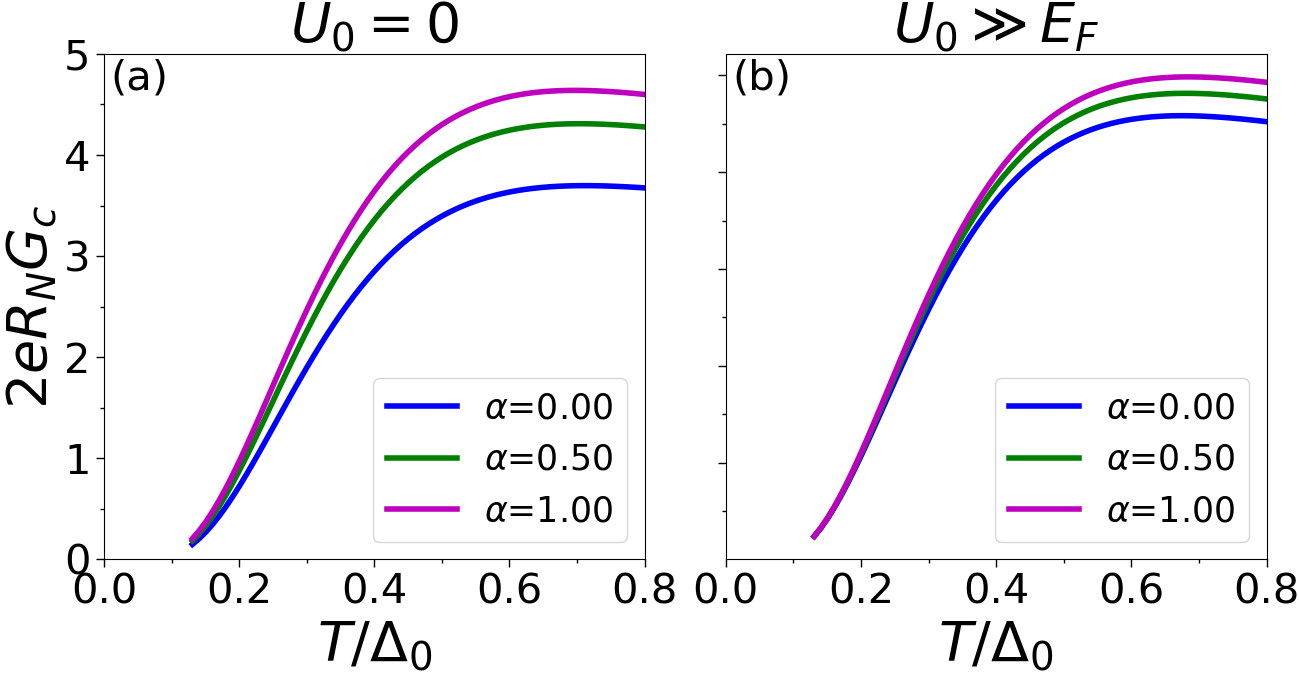
Furthermore, from Eq.(25) we can see that “figure of merit” , which defines the efficiency of this system as a thermopower device, depends upon the Seebeck coefficient , the charge conductance , and the thermal conductance . To understand the effect of charge and thermal conductance on , we show the results of the charge and the thermal conductance of the based NIS junction. In Fig.6 we present the variation of a dimensionless quantity, as a function of temperature (scaled by ) for a fixed value of for two different cases (see Fig.6a), and (see Fig.6b). Here increases monotonically with an increase in and after attaining a certain values it saturates for all values of for both the cases. Unlike the Seebeck coefficient, the maxima of the charge conductance increases with the increase of for both the cases.
D. Thermal Conductance:
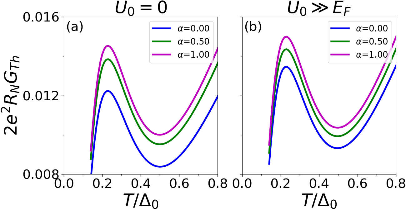
In Fig.7 we present the variation of a dimensionless quantity, as a function of temperature (scaled by ) for a fixed value of for two different cases (see Fig.7a), and (see Fig.7b). Here increases rapidly with an increase of in the low temperature regime. After attaining a maximum value (where the Seebeck coefficient attains maxima), it decreases, and after attaining a minimum value (where the charge conductance gets maxima), it again increases with temperature for all values of for both the cases. Here, unlike the Seebeck coefficient, the maxima of thermal conductance increases with the increase of for both the cases.
E. Figure of Merit:
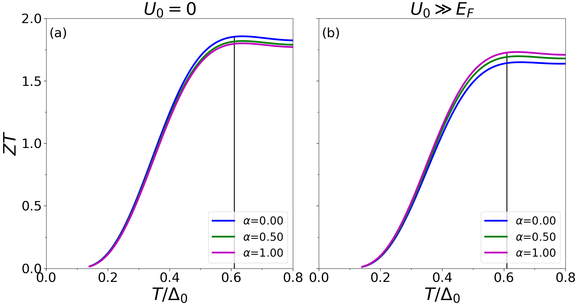
Now the variation of the figure of merit, as a function of temperature (in units of the superconducting gap, ) is shown in the Fig.8. It shows that initially with temperature the efficiency of the system increases, attains a maximum value at and then decreases. For the Fermi surface matched condition, that is, (Fig.8a) the maximum efficiency of the NIS junction device decreases as we increase the strength of the parameter from to . Further, for the Fermi surface mismatch condition i.e., (Fig.8b), the maximum efficiency increases as we increase the value of . Thus, for two different cases, the figure of merit follows the same trend as that of the Seebeck coefficient as a function of .
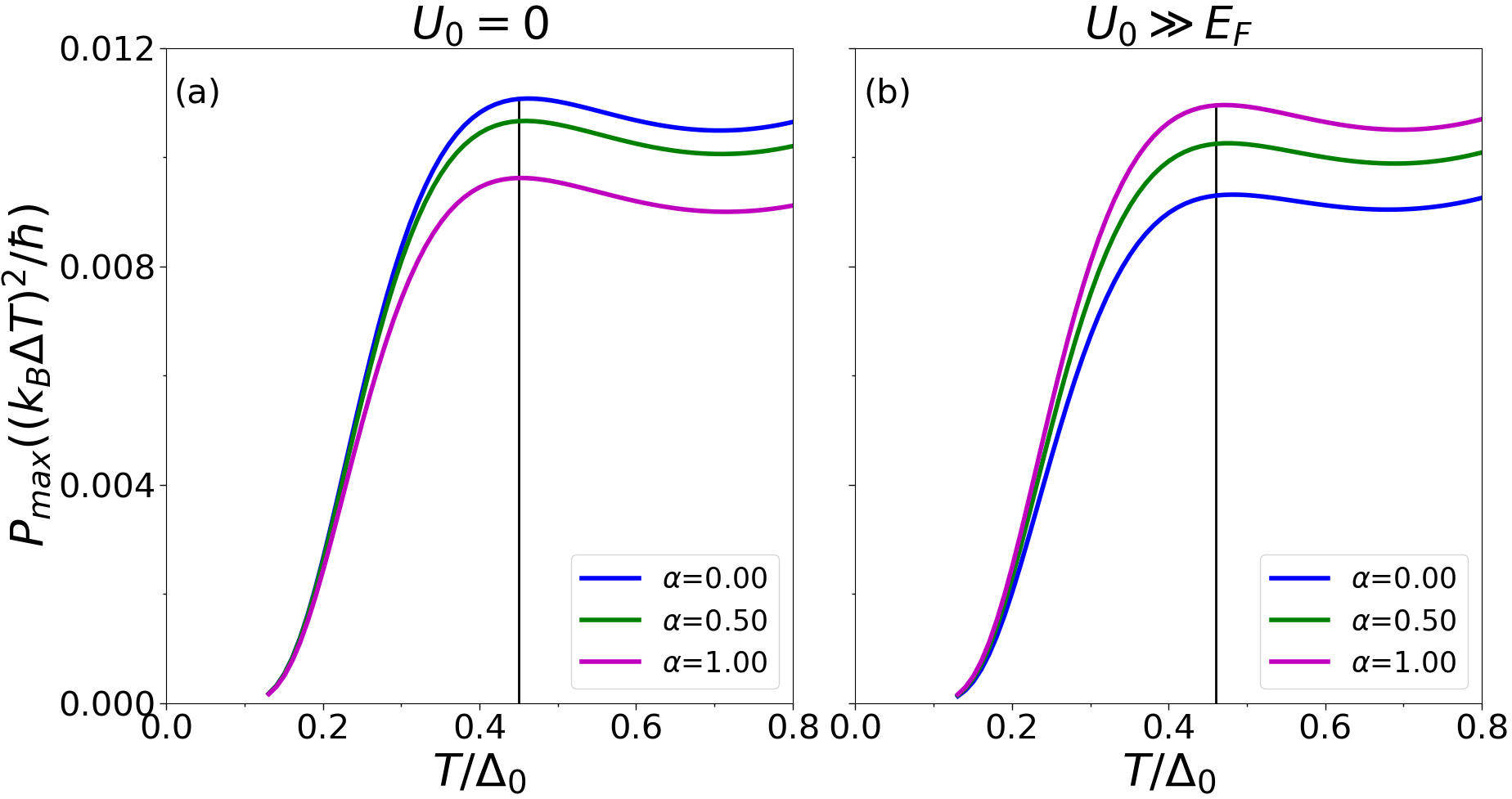
F. Maximum Power:
The maximum power is plotted as a function of temperature in Fig.9. As earlier, here also we consider two cases: for (Fig.9a), and for (Fig.9b). The maximum power follows the same trend as that of the Seebeck coefficient. We can see that the maximum power is obtained where the Seebeck coefficients get their maximum value irrespective of the value. The maximum power is obtained at the temperature () for all two cases mentioned above and for all values of the parameter . As earlier, we observe that the maximum power decreases with the increasing strength of for , while for , the reverse trend is obtained.
G. Efficiency at Maximum Power:
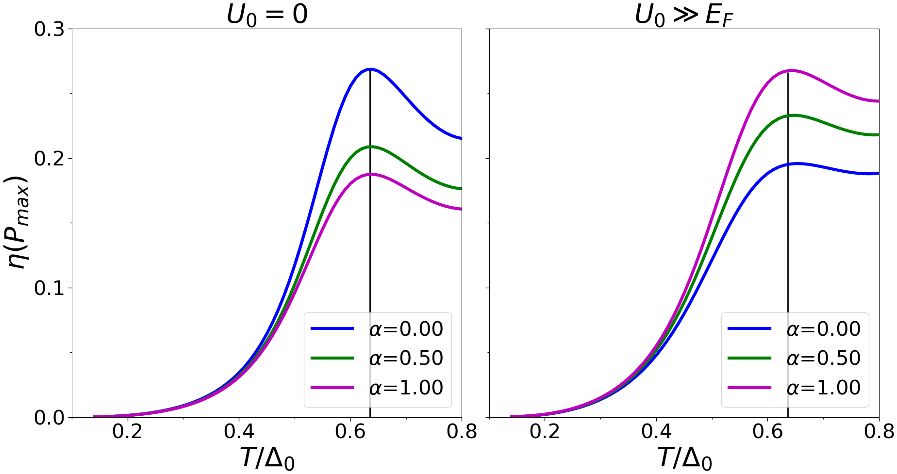
From Eq.(24) we can see that the maximum efficiency of the system depends upon the figure of merit of the system. In Fig.10 we present the efficiency for two pre-defined cases (see Fig.10a and Fig.10b). The efficiency when the system operates at the maximum power follows the same trend as that of the figure of merit and the Seebeck coefficient as is varied. Thus, the best efficiency is obtained whenever the temperature () is for the two different cases and all values of parameter .
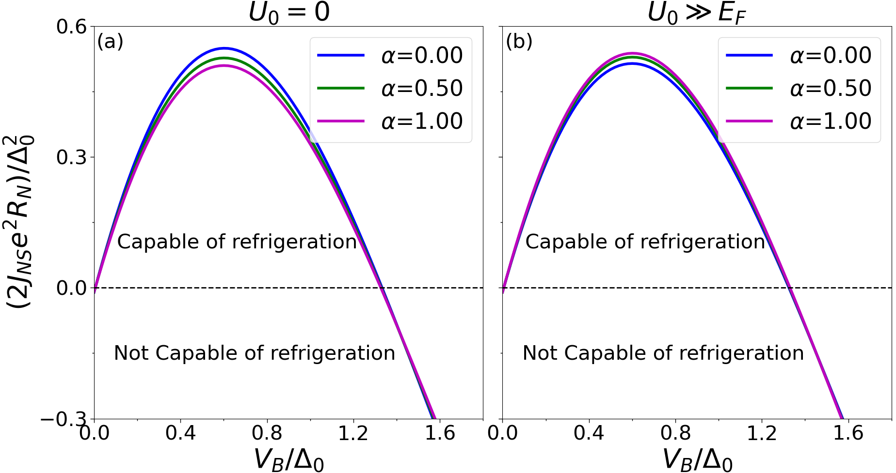
H. Thermoelectric Cooling: Here, we show the results of the thermoelectric cooling of the based NIS junction. Fig.11 presents the variation of a dimensionless quantity ( being the thermal current) as a function of the biasing voltage (in units of the superconducting gap ), for a fixed where the temperature is fixed at . It is observed that at zero bias voltage, the rate of the thermal current extracted from the cold (normal) reservoir is negative. To achieve cooling effects, a lower threshold voltage of the battery, namely, is needed. Also beyond an upper threshold voltage , the refrigeration effect does not exist. For a very small range of the biasing voltage (-), the thermoelectric cooling process is efficient and the maximum refrigeration occurs at around, for all values of . Further, the maximum refrigeration decreases as we increase the strength of the parameter for case (Fig. 11a). Furthermore, for the Fermi surface mismatch condition i.e., for , (Fig. 11b) the maximum refrigeration increases as we increase the strength of the parameter.
IV Conclusions
In conclusion, we discuss the tunneling conductance of based NIS junctions. We have demonstrated that the tunneling conductance exhibits periodic oscillatory behavior as a function of the barrier strength of the junction. The periodicity and the amplitudes of the oscillations depend on and as well as on the values of . We have investigated the Seebeck coefficient, the thermoelectric figure of merit, maximum power, and the efficiency at maximum power of this junction device and explained how plays a role in determining these properties. Further, the thermoelectric cooling of this junction device have been studied in details. We have ascertained whether a graphene or a dice lattice is more suitable for a thermoelectric device, and the answer depends on the superconducting potential . We observe that for , graphene () is more feasible for constructing a thermoelectric device, whereas for , the dice lattice () is more suitable candidate. Since the effective barrier potential (), the superconducting potential , and the hopping strength can be tuned by external means, our study on the conductance and thermoelectric properties can be important inputs to the experimental studies that aim to provide the desired conductance and thermoelectric properties of based NIS junction devices.
Acknowledgements
MI and PK gratefully acknowledge Prof. S. Basu for useful discussions.
References
- [1] K. S. Novoselov, A. K. Geim, S. V. Morozov, D. Jiang , M. I. Katsnelson, I. V. Grigorieva, S. V. Dubonos and A. A. Firsov, Nature, 438, 197 (2005).
- [2] A. De Martino, L. DellAnna and R. Egger, Phys. Rev. Lett., 98, 066802 (2007).
- [3] Y. Zhang, Y. W. Tan, H. L. Stormer and P. Kim, Nature, 438, 201 (2005).
- [4] K. S. Novoselov, Z. Jiang, Y. Zhang , S. V. Morozov, H. L. Stormer, U. Zeitler, J. C. Maan, G. S. Boebinger, P. Kim and A. K. Geim, Science, 315, 1379 (2007).
- [5] M. I. Katsnelson, K. S. Novoselov and A. K. Geim, Nat. Phys., 2, 620 (2006).
- [6] C. W. J, Beenakker, Rev. Mod. Phys., 80 1337, (2008).
- [7] M. Zareyan, H. Mohammadpour and A. G. Moghaddam, Phys. Rev. B 78, 193406 (2008).
- [8] A. H. C. Neto, F. Guinea, N. M. R. Peres, K. S. Novoselov and A. K. Geim Rev. Mod. Phys. 81 109 (2009).
- [9] F. Bonaccorso, Z. Sun, T. Hasan and A. C. Ferrari, Nat. Photon. 4 611 (2010).
- [10] P. Avouris , Nano. Lett. 10 4285 (2010).
- [11] A. G. Moghaddam and M. Zareyan M., Phys. Rev. Lett. 105 146803 (2010).
- [12] D. Pesin and A. H. MacDonald, Nat. Mater 11 409 (2012).
- [13] B. Ghosh, J. Appl. Phys., 109 013706 (2011).
- [14] M. I. Katsnelson, Graphene: Carbon in Two Dimensions (Cambridge University Press, Cambridge, 2012).
- [15] B. Sutherland, Phys. Rev. B 34, 5208 (1986).
- [16] J. Vidal, R. Mosseri, and B. Doucot, Phys. Rev. Lett. 81, 5888 (1998).
- [17] S. E. Korshunov, Phys. Rev. B 63, 134503 (2001).
- [18] M. Rizzi, V. Cataudella, and R. Fazio, Phys. Rev. B 73, 144511 (2006)
- [19] D. F. Urban, D. Bercioux, M. Wimmer, and W. Häusler, Phys. Rev. B 84, 115136 (2011).
- [20] J. D. Malcolm and E. J. Nicol, Phys. Rev. B 93, 165433 (2016).
- [21] D. Bercioux, D. F. Urban, H. Grabert, and W. Hausler, Phys. Rev. A 80, 063603 (2009).
- [22] M. Vigh, L. Oroszlány, S. Vajna, P. San-Jose, G. Dávid, J. Cserti, and B. Dóra, Phys. Rev. B 88, 161413(R) (2013).
- [23] F. Wang and Y. Ran, Phys. Rev. B 84, 241103 (2011).
- [24] J. D. Malcolm and E. J. Nicol, Phys. Rev. B 92, 035118 (2015).
- [25] E. Illes, J. P. Carbotte, and E. J. Nicol, Phys. Rev. B 92, 245410 (2015).
- [26] E. Illes and E. J. Nicol, Phys. Rev. B 94, 125435 (2016).
- [27] T. Biswas and T. K. Ghosh, J. Phys.: Condens. Matter 28, 495302 (2016).
- [28] T. Biswas and T. K. Ghosh, J. Phys.: Condens. Matter 30, 075301 (2018).
- [29] S. K. Firoz Islam and P. Dutta, Phys. Rev. B 96, 045418 (2017).
- [30] B. Dey and T. K. Ghosh, Phys. Rev. B 98, 075422 (2018).
- [31] T. Louvet, P. Delplace, A. A. Fedorenko, and D. Carpentier, Phys. Rev. B 92, 155116 (2015).
- [32] J. Wang, J. F. Liu, and C. S. Ting, Phys. Rev. B 101, 205420 (2020).
- [33] R. Shen, L. B. Shao, B. Wang, and D. Y. Xing, Phys. Rev. B 81, 041410(R) (2010).
- [34] D. F. Urban, D. Bercioux, M. Wimmer, and W. Häusler, Phys. Rev. B 84, 115136 (2011).
- [35] E. Illes and E. J. Nicol, Phys. Rev. B 95, 235432 (2017).
- [36] Y. Betancur-Ocampo, G. Cordourier-Maruri, V. Gupta, and R. de Coss, Phys. Rev. B 96, 024304 (2017).
- [37] E. V. Gorbar, V. P. Gusynin, and D. O. Oriekhov, Phys. Rev. B 99, 155124 (2019).
- [38] E. V. Gorbar, V. P. Gusynin, and D. O. Oriekhov, Phys. Rev. B 103, 155155 (2021).
- [39] L. Chen, J. Zuber, Z. Ma, and C. Zhang, Phys. Rev. B 100, 035440 (2019).
- [40] D. Bercioux, N. Goldman, and D. F. Urban, Phys. Rev. A 83, 023609 (2011).
- [41] B. Dey and T. K. Ghosh, Phys. Rev. B 99, 205429 (2019).
- [42] B. Dey, P. Kapri, O. Pal, and T. K. Ghosh, Phys. Rev. B 101, 235406 (2020).
- [43] S. Cheng, H. Yin, Z. Lu, C. He, P. Wang, and G. Xianlong, Phys. Rev. A 101, 043620 (2020).
- [44] J. Wang and J.-F. Liu, Phys. Rev. B 103, 075419 (2021).
- [45] A. Iurov, G. Gumbs, and D. Huang, Phys. Rev. B 99, 205135 (2019).
- [46] A. Iurov, L. Zhemchuzhna, D. Dahal, G. Gumbs, and D. Huang, Phys. Rev. B 101, 035129 (2020).
- [47] M.-W. Alam, B. Souayeh, and S. K. Firoz Islam, J. Phys.: Condens. Matter 31, 485303 (2019).
- [48] E. Tang, J.-W. Mei, and X.-G. Wen, Phys. Rev. Lett. 106, 236802 (2011).
- [49] K. Sun, Z. Gu, H. Katsura, and S. Das Sarma, Phys. Rev. Lett. 106, 236803 (2011).
- [50] T. Neupert, L. Santos, C. Chamon, and C. Mudry, Phys. Rev. Lett. 106, 236804 (2011).
- [51] Z. Liu, Z.-F. Wang, J.-W. Mei, Y.-S. Wu, and F. Liu, Phys. Rev. Lett. 110, 106804 (2013).
- [52] M. G. Yamada, T. Soejima, N. Tsuji, D. Hirai, M. Dinca, and H. Aoki, Phys. Rev. B 94, 081102(R) (2016).
- [53] N. Su, W. Jiang, Z. Wang, and F. Liu, Appl. Phys. Lett. 112, 033301 (2018).
- [54] J. W. McClure, Phys. Rev. 104, 666–671 (1956).
- [55] P. Kapri and S. Basu, EPL. 124 (2018) 17002.
- [56] J. Mastomaki, S. Roddaro, M. Rocci, V. Zannier, D. Ercolani, L. Sorba, I. J. Maasilta, N. Ligato, A. Fornieri, E. Strambini and F. Giazotto, Nano Res. 10, 3468 (2017).
- [57] M. Nahum, T. M. Eiles and J. M. Martinis, Appl. Phys. Lett. 65, 3123 (1994).
- [58] M. Wysokinski, Acta Phys. Pol. A 122, 163905 (2012).
- [59] M. Wysokinski and J. Spalek, J. Appl. Phys. 113, 163905 (2013).
- [60] P. Kapri and S. Basu, Eur. Phys. J. B (2017) 90:33.
- [61] P. Kapri and S. Basu, EPL. 125 (2019) 47003.
- [62] P. Kapri , Physica E: Low-dimensional Systems and Nanostructures 99 (2018) 67–74.
- [63] P. Kapri and S. Basu, Physica E: Low-dimensional Systems and Nanostructures 103 (2018) 383–390.
- [64] A. V. Feshchenko, J. V. Koski and J. P. Pekola, Phys. Rev. B 90, 201407(R) (2014).
- [65] A. M. Clark, A. Williams, S. T. Ruggiero, M. L. Berg and J. N. Ullom, Appl. Phys. Lett. 84, 625 (2004).
- [66] N. A. Miller, G. C. ONeil, J. A. Beall, G. C. Hilton, K. D. Irwin, D. R. Schmidt, L. R. Vale and J. N. Ullom, Appl. Phys. Lett. 92, 163501 (2008).
- [67] K. S. Novoselov , Nature (London) 438, 197 (2005).
- [68] Y. Zhang , Nature (London) 438, 201 (2005).
- [69] K. S. Novoselov , Nature Phys. 2, 177 (2006).
- [70] M. I. Katsnelson , Nature Phys. 2, 620 (2006).
- [71] C. W. J. Beenakker, Phys. Rev. Lett. 97, 067007 (2006).
- [72] A. F. Volkov , Physica C (Amsterdam) 242, 261 (1995).
- [73] S. Bhattacharjee and K. Sengupta, Phys. Rev. Lett. 97, 217001 (2006).
- [74] X. Zhou, Phys. Rev. B 104, 125441 (2021).
- [75] H. Li, Phys. Rev. B 94, 075428 (2016).
- [76] H. Li, G. Ouyang, Phys. Rev. B 100, 085410 (2019).
- [77] A. Mawrie, and B. Muralidharan, Phys. Rev. B. 100, 081403 (R) (2019).
- [78] G. S. Nolas, J. Sharp, and H. J. Goldsmid, Basic Principles and New Materials Developments (Springer, Berlin, 2001).