Flash-Cosmos: In-Flash Bulk Bitwise Operations Using
Inherent Computation Capability of NAND Flash Memory
Abstract
Bulk bitwise operations, i.e., bitwise operations on large bit vectors, are prevalent in a wide range of important application domains, including databases, graph processing, genome analysis, cryptography, and hyper-dimensional computing. In conventional systems, the performance and energy efficiency of bulk bitwise operations are bottlenecked by data movement between the compute units (e.g., CPUs and GPUs) and the memory hierarchy. In-flash processing (i.e., processing data inside NAND flash chips) has a high potential to accelerate bulk bitwise operations by fundamentally reducing data movement through the entire memory hierarchy, especially when the processed data does not fit into main memory.
We identify two key limitations of the state-of-the-art in-flash processing technique for bulk bitwise operations; (i) it falls short of maximally exploiting the bit-level parallelism of bulk bitwise operations that could be enabled by leveraging the unique cell-array architecture and operating principles of NAND flash memory; (ii) it is unreliable because it is not designed to take into account the highly error-prone nature of NAND flash memory.
We propose Flash-Cosmos (Flash Computation with One-Shot Multi-Operand Sensing), a new in-flash processing technique that significantly increases the performance and energy efficiency of bulk bitwise operations while providing high reliability. Flash-Cosmos introduces two key mechanisms that can be easily supported in modern NAND flash chips: (i) Multi-Wordline Sensing (MWS), which enables bulk bitwise operations on a large number of operands (tens of operands) with a single sensing operation, and (ii) Enhanced SLC-mode Programming (ESP), which enables reliable computation inside NAND flash memory. We demonstrate the feasibility of performing bulk bitwise operations with high reliability in Flash-Cosmos by testing 160 real 3D NAND flash chips. Our evaluation shows that Flash-Cosmos improves average performance and energy efficiency by 3.5/32 and 3.3/95, respectively, over the state-of-the-art in-flash/outside-storage processing techniques across three real-world applications.
1 Introduction
Many data-intensive applications rely on bulk bitwise operations, i.e., bitwise operations on large bit vectors. As such, it is important for modern computing systems to support high-performance and energy-efficient bulk bitwise operations. In databases and web search, prior works (e.g., [1, 2, 3, 4, 5, 6, 7, 8, 9]) propose various techniques that heavily use bulk bitwise operations to accelerate queries. Bulk bitwise operations are also prevalent in various other important application domains, including databases and web search [1, 2, 3, 4, 5, 6, 7, 8, 9, 10, 11, 12, 13], data analytics [14, 7, 15, 16, 17], graph processing [18, 19, 20, 21, 9], genome analysis [22, 23, 24, 25, 26, 27, 28, 29], cryptography [30, 31, 32], set operations [19, 7], and hyper-dimensional computing [33, 34, 35, 36].
In conventional systems, the performance and energy efficiency of bulk bitwise operations are bottlenecked by data movement between the compute units (e.g., CPUs or GPUs) and the memory hierarchy [37, 8, 7, 21, 20, 38, 39]. To perform a bulk bitwise operation, a conventional system must first move every operand to the compute unit and eventually write the results back into the memory hierarchy. Due to the simple nature of bitwise operations, such data movement dominates the execution time and energy consumption in bulk bitwise operations.
Processing data inside NAND flash chips, i.e., in-flash processing (IFP), can fundamentally reduce the data movement that bottlenecks the execution of bulk bitwise operations. IFP is an instance of near-data processing (NDP), a computing paradigm that moves computation closer to where the data resides (e.g., [37, 40, 41, 42, 8, 7, 43, 44, 45, 46, 47, 48, 9, 20, 49, 50, 51, 52, 21, 53, 54]). When processing large amounts of data that do not fit in main memory, IFP significantly reduces data movement across the entire memory hierarchy by performing computation within the underlying storage media (i.e., NAND flash chips) and transferring only the result (when needed, to main memory and CPUs/GPUs). As we discuss in Section 3, IFP can significantly outperform in-storage processing (ISP) approaches that leverage hardware accelerators inside the NAND flash-based solid-state drive (SSD) (e.g., [49, 50, 51, 52, 55, 56]), by reducing data movement to/from NAND flash chips.
To our knowledge, only one recent work, ParaBit [21], proposes an in-flash processing technique for bulk bitwise operations.111 There are many prior works (e.g., [57, 58, 59, 60, 61, 62, 63]) that leverage analog current sensing to perform accumulative computation (e.g., multiply-accumulate operation) inside NAND flash chips. However, these proposals 1) use NAND flash memory solely as an accelerator but not as a storage medium, and 2) require significant changes (e.g., adding a precise analog-to-digital converter to each bitline) to commodity NAND flash chips, which increases cost. See Section 9 for more detail. We identify that ParaBit has two major limitations. First, ParaBit falls greatly short of exploiting the full potential of NAND flash memory to significantly improve the performance and energy efficiency of bulk bitwise operations. To perform bulk bitwise operations for more than two operands (e.g., A B C), which frequently happens in many data-intensive applications such as data analytics [14, 7, 15, 16, 17], databases [10, 11, 12, 13] and graph processing [20, 21, 19, 9], ParaBit must serially perform multiple two-operand bitwise operations (e.g., (A B) C). Doing so requires multiple long-latency sensing operations in series, which become a new performance and energy efficiency bottleneck. In this work, we observe that NAND flash memory has inherent capability to perform bitwise operations on a large number (e.g., tens) of operands at once (i.e., with a single sensing operation) due to its unique cell-array structures that are similar to digital logic circuits for NAND and NOR gates.
Second, ParaBit is applicable only to highly error-tolerant applications because it is not designed to take into account the highly error-prone nature of NAND flash memory. To ensure data reliability, modern NAND flash-based SSDs commonly use (i) error-correcting codes (ECC) and (ii) data randomization [64, 65, 66, 67]. Unfortunately, ParaBit cannot leverage any of the widely-used ECC and data-randomization techniques, as it performs bitwise operations while sensing the cells that store the data. Performing bitwise AND and OR operations on ECC-encoded or randomized data using ParaBit can lead to incorrect results during ECC decoding and/or de-randomization. Although storing a smaller number of bits in a cell would reduce the raw bit error rate (RBER) of NAND flash memory, our characterization using 160 real 3D NAND flash chips shows that even storing a single bit per cell cannot provide sufficiently-low RBER for ParaBit to be adopted across a wide range of applications.
Our goal is to improve both the performance and energy efficiency of in-flash bulk bitwise operations while ensuring high reliability (i.e., zero bit errors) in computation results. To this end, we propose Flash-Cosmos (Flash Computation with One-Shot Multi-Operand Sensing), a novel in-flash processing technique for bulk bitwise operations that achieves our goal by exploitingtwo key ideas: (i) Multi-Wordline Sensing (MWS), which enables in-flash bulk bitwise operations on multiple (e.g., tens) operands with a single sensing operation, and (ii) Enhanced SLC-mode Programming (ESP), which effectively achieves zero bit errors in the results of in-flash bulk bitwise operations.
MWS leverages the two fundamental cell-array structures of NAND flash memory to perform in-flash bulk bitwise operations on a large number of operands with a single sensing operation: (i) a number of flash cells (e.g., 24–176 cells) are serially connected to form a NAND string (similar to digital NAND logic); (ii) thousands of NAND strings are connected to the same bitline (similar to digital NOR logic). Under these cell-array structures, simultaneously sensing multiple wordlines222 NAND flash memory concurrently reads a large number of () cells whose control gates are connected to the same wordline. See Section 2.1 for more background on NAND flash memory operation. automatically results in (i) bitwise AND of all the sensed wordlines if they are in the same NAND string or (ii) bitwise OR of all the wordlines if they are in different NAND strings.
ESP effectively avoids raw bit errors in stored data via more precise programming-voltage control. A flash cell stores bit data as a function of the level of its threshold-voltage (V). Reading a cell incurs an error if the cell’s V level moves to another V range that corresponds to a different bit value than the stored value, due to various reasons [67], such as program interference [68, 69, 70], data retention loss [71, 72, 73, 74], read disturbance [75, 76], and cell-to-cell interference [69]. ESP maximizes the margin between different V ranges by carefully leveraging two existing approaches. First, to store data for in-flash processing, it uses the single-level cell (SLC)-mode programming scheme [77, 78]. Doing so guarantees a large V margin by forming only two V ranges (for encoding ‘1’ and ‘0’) within the fixed V window. Second, ESP enhances the SLC-mode programming scheme by using (i) a higher programming voltage to increase the distance between the two V ranges and (ii) more programming steps to narrow the high V range. While many prior works also leverage precise programming to enhance the reliability of NAND flash memory [79, 80, 81, 82, 83, 84], we aim to achieve zero bit errors in computation results and demonstrate that doing so is possible in modern NAND flash memory by combining the two approaches that comprise ESP.
In this paper, we enhance our basic MWS mechanism in two ways to make it more general purpose. First, we support bitwise NAND/NOR/XOR/XNOR by using MWS along with (i) the inverse sensing mechanism [85, 86] and (ii) internal XOR logic [87, 88], both of which are already supported in most NAND flash chips. Second, we relax the data location constraints of the basic MWS mechanism (e.g., bitwise OR/NOR operations are possible only for wordlines in different NAND strings) by (i) storing each operand’s inverse data and (ii) leveraging De Morgan’s laws. For example, if the user stores the inverse of A, B, and C (i.e., , , and ) in the same NAND string, Flash-Cosmos can perform bitwise OR of three wordlines by performing bitwise NAND of , , and because (A OR B OR C)NOT ( AND AND ).
Flash-Cosmos requires only small changes to the control logic of a NAND flash chip, but no changes to its cell array and sensing circuitry. For efficient post-fabrication tests and optimizations, most modern NAND flash chips are already capable of (i) simultaneously sensing multiple wordlines [89] and (ii) adjusting programming step and voltage at fine granularity [79, 81, 90, 67]. Hence, integrating Flash-Cosmos into existing NAND flash chips requires changes only to the command latching circuitry and the firmware of the microcontroller in the flash chip (see Section 6).
We evaluate Flash-Cosmos in two ways. First, we validate Flash-Cosmos using 160 real 48-layer 3D NAND flash chips. Our results show that Flash-Cosmos enables commodity NAND flash chips to perform bitwise AND/OR/NAND/NOR of up to 48 operands via a single sensing operation (25 µs). In our validation of computation results across more than 1011 flash cells, we observe zero bit errors. Second, we compare Flash-Cosmos to two different computing platforms, a state-of-the-art multi-core CPU (which we call outside-storage processing or OSP) [91] and ParaBit [21]. Our evaluation using three real-world workloads shows that Flash-Cosmos improves performance by 32/3.5 and reduces energy consumption by 95/3.3 on average compared to OSP/ParaBit.
This work makes the following key contributions:
-
•
To our knowledge, this work is the first to enable NAND flash memory to perform bulk bitwise operations on multiple (i.e., tens) operands via a single sensing operation.
-
•
We introduce Flash-Cosmos, a new in-flash processing technique to significantly improve both performance and energy efficiency of bulk bitwise operations while achieving zero bit errors in computation results.
-
•
We demonstrate the feasibility and reliability of Flash-Cosmos using 160 real state-of-the-art 3D NAND flash chips.
-
•
We evaluate the effectiveness of Flash-Cosmos using real-world workloads, showing large performance and energy benefits over a state-of-the-art multi-core processor and the state-of-the-art in-flash processing technique.
2 Background
We provide a brief background on NAND flash memory that is useful to understand the rest of the paper.
2.1 Basics of NAND Flash Memory
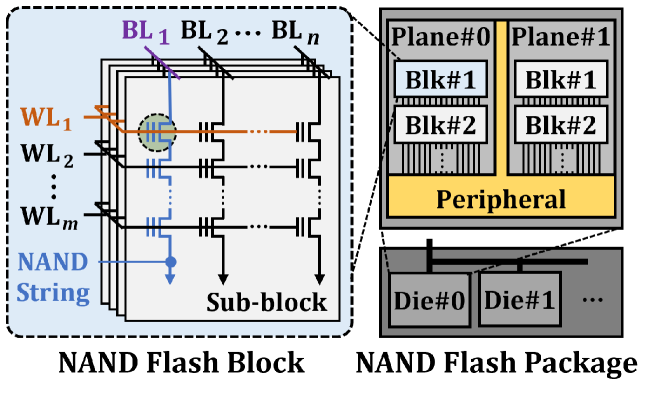
NAND Flash Organization. Figure 1 shows the organization of 3D NAND flash memory. A number of vertically-stacked flash cells (e.g., 24 to 176 cells) are serially connected, which is called a NAND string. A NAND string is connected to a bitline (BL), and NAND strings at different BLs compose a sub-block. The control gates of all cells that are at the same vertical location in a sub-block are connected to the same wordline (WL), which makes all such cells operate concurrently. A NAND flash block consists of several (e.g., 4 or 8) sub-blocks, and thousands of blocks comprise a plane. The blocks in a plane share all the BLs in that plane, which implies that a single BL is shared by thousands of NAND strings. In the rest of the paper, unless specified otherwise, we refer to a sub-block as a block for simplicity. A NAND flash chip (or a die) contains multiple (e.g., 2 or 4) planes. Multiple chips in a NAND flash package can operate independently of each other but share the package’s command/data buses (i.e., channel) in a time-interleaved manner.
Program and Erase Operations. A flash cell stores data using its threshold voltage (V) level that highly depends on the amount of charge in the cell’s charge trap. A program operation injects electrons into a cell, which increases the cell’s V level. As multiple flash cells are connected to a single WL, NAND flash memory writes data at page (e.g., 16 KiB) granularity such that each cell in a WL stores one bit of the page. To decrease a programmed cell’s V level, NAND flash memory performs an erase operation that ejects electrons from the cell. The granularity of an erase operation is a block, which causes the erase latency tBERS to be much longer (e.g., 3–5 ms) than the program latency tPROG (e.g., 200–700 µs).
Read Operation. NAND flash memory determines a cell’s V level (i.e., the cell’s bit data) by sensing the conductance of the corresponding NAND string. Figure 2 shows the read mechanism of NAND flash memory, which consists of three steps: (i) precharge, (ii) evaluation, and (iii) discharge [92, 64]. In the precharge step ( in the left part of Figure 2), a NAND flash chip charges all target BLs and their sense-out (SO) capacitors (C) to the precharge voltage V by enabling the precharge transistor M . At the same time, the chip applies the read-reference voltage V to the target WL while applying a much larger pass voltage V to the other WLs in the same block . Doing so makes each target cell’s V level dictate the corresponding NAND string’s conductance; the target cell would operate as either a resistor, if VV ( in Figure 2, left part), or an open switch, if VV ( ); all non-target cells in the same NAND string would always operate as resistors since V is high enough (6 V) to turn on any flash cell regardless of its V level [75]. The chip then starts the evaluation of the target cells ( in the middle part of Figure 2) by disconnecting the BLs from V and enabling the latching circuit . If the target cell’s V level is lower than V, the charge in C quickly flows through the NAND string ( ), which is sensed as a ‘1’. If VV, the capacitance of C hardly changes ( ) as the target cell blocks the BL discharge current, which is sensed as a ‘0’. Finally, the chip discharges the BLs ( in the right part of Figure 2) to return the NAND string to its initial stable state (i.e., the state before precharge can take place) for future operations.
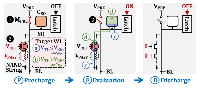
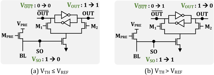
Figure 3 depicts how NAND flash memory senses a BL’s conductance with its latching circuit. Figures 3(a) and 3(b) describe the operation of the latching circuit when the threshold voltage V of a flash cell is lower and higher than the read reference voltage V, respectively. We show the transition in voltage state at each of the three nodes (SO/OUT/) when going from the precharge step ( in Figure 2) to the evaluation step ( in Figure 2). During precharge, the NAND flash chip charges the BL, making V1. Before the evaluation step, the chip initializes the latching circuit by activating only transistor M1, resulting in V0 and thus V1. The evaluation step disables M and M1 while enabling M2. In Figure 3(a), the evaluation step makes V0 as the charge in C quickly flows through the NAND string (because VV), which leads to V1 ( in Figure 2). The bit value of the flash cell is immediately stored in the latching circuit because of the low charge retention of C [92]. In Figure 3(b), the evaluation step leads to V1 and V0 as the flash cell operates as an open switch when VV.
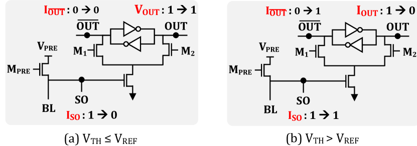
Inverse Read. Modern NAND flash chips commonly support the inverse-read mode [85] to read the inverse of the stored data.333 Supporting inverse reads is essential to the copyback operation [85] that moves a page’s data to another page in the same plane without off-chip data transfer and thus can improve SSD garbage-collection performance [93, 94]. Supporting inverse reads requires no hardware changes to the latching circuit shown in Figure 4. We denote the voltage states at the three nodes (SO/OUT/) during an inverse read operation using I, I and I. The chip performs an inverse read by simply changing the activation sequence of M1 and M2. Unlike a read operation, the inverse read activates M2 to initialize the latching circuit before the evaluation step. This leads to I0 and thus I1. During the evaluation step, M1 is activated while MPRE and M2 are disabled. This causes the values stored in the latching circuit after the evaluation step to be the inverse of the values stored in a normal read.
2.2 Reliability of NAND Flash Memory
Modern NAND flash memory is highly error-prone due to various error sources [67] such as program interference [68, 69, 70], data retention loss [71, 72, 73, 74], read disturbance [75, 76], and cell-to-cell interference [69]. Figure 5 shows the V distribution of a WL, when the WL is programmed in (a) single-level cell (SLC) mode and (b) multi-level cell (MLC) mode to store one and two bits per cell, respectively. Reading or programming a WL affects the V distribution of other WLs in the same block by increasing the V level of other cells (i.e., interference and disturbance as shown in Figure 5(a)). A flash cell also leaks its charge over time, which decreases its V level (i.e., retention loss as shown in Figure 5(a)). If a cell’s V level moves beyond V (i.e., to a V range corresponding to a different value), sensing the cell results in a different value from the original stored data, introducing a bit error.
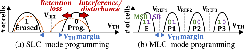
Two major factors significantly increase the raw (i.e., pre-correction) bit-error rate (RBER) of NAND flash memory. First, a flash cell becomes more error-prone as it experiences more program and erase (P/E) cycles [95], due to the high voltage used in program and erase operations which damages the cell to more easily leak its charge. Second, storing more bits per cell increases RBER because it reduces the margin between adjacent V ranges in order to pack more V states within the same voltage window, as shown in Figure 5(b).
Error-Correcting Codes (ECC). To ensure the integrity of stored data, modern SSDs commonly employ ECC. ECC can detect and correct bit errors by storing redundant information. To cope with the high RBER of modern NAND flash memory, it is necessary to use sophisticated ECC (e.g., low-density parity-check (LDPC) codes [96, 97, 67, 98, 99, 100, 101]), which increases the performance and the area overheads of an ECC engine.
Data Randomization. It is common practice to randomize the values of stored data in modern SSDs to reduce the probability of worst-case data patterns that would exacerbate program disturbance [102, 87, 66]. For example, when a NAND string has many consecutive erased cells, programming the next cell of the same NAND string significantly increases the V level of the consecutive cells, which could introduce bit errors. Data randomization reduces the probability of such cases to a small value by randomly distributing V states across a NAND string regardless of the original data values to store.444In fact, randomization is the reason why the V distribution of NAND flash memory is commonly described by using V states with the same shape, as in Figure 5. The stored data is de-randomized during a read operation to correctly read the originally stored values before they were randomized.
3 Motivation
We describe the benefits of in-flash processing and the main limitations of the state-of-the-art in-flash processing technique for bulk bitwise operations (i.e., bitwise operations on large bit vectors) [21].
3.1 In-Flash Bulk Bitwise Operations
Many prior studies [7, 37, 48, 20, 9, 8, 38] investigate near-data processing (NDP) solutions for bulk bitwise operations due to two main reasons.
First, bulk bitwise operations are used in a wide variety of important applications, including databases and web search [1, 2, 3, 4, 5, 6, 7, 8, 9, 10, 11, 12, 13],
data analytics [14, 7, 15, 16, 17],
graph processing [18, 19, 20, 21, 9], genome analysis [22, 23, 24, 25, 26, 27, 28, 29], cryptography [30, 31, 32], set operations [19, 7], and hyper-dimensional computing [33, 34, 35, 36].
Second, bulk bitwise operations can significantly benefit from NDP.
Due to the simple nature of bitwise operations, the performance and energy efficiency of bulk bitwise operations are bottlenecked by data movement between the computation units and the memory hierarchy in conventional systems [37, 8, 7, 21, 9, 38].
NDP can effectively mitigate such data movement at low cost by supporting simple bulk bitwise operations at very high levels of concurrency near or inside memory devices (e.g., in all memory banks or subarrays [7, 9, 103]).
Among many existing NDP solutions, only one recent work, ParaBit [21], proposes an in-flash processing technique for bulk bitwise operations inside a NAND flash chip. ParaBit leverages the latching circuits that are commonly employed in modern NAND flash chips [104, 105, 106, 107, 108, 92] (see Section 2.1).
Existing NAND flash chips support a command called cache read [104, 105, 106, 107, 108] whose purpose is to improve the performance of a read operation by enabling the transfer of data from the NAND flash chip to the flash controller in parallel with the sensing of a subsequent read operation.
To enable cache read, existing chips include a cache latch in addition to the sensing latch ( in Figure 2).
We describe the operation and implementation of this cache latch since it is important for and used in Parabit.
Figure 6(a) illustrates the common latching circuit of a modern NAND flash chip equipped with a cache latch (right part) in addition to the sensing latch (left part) described in Figure 3.
A NAND flash chip initializes the cache latch in the precharge step by activating M, which pulls down node OUT and thus makes 1.
Until enabling M, the sensing latch (i.e., the value at node OUT) cannot affect the data stored in the cache latch.
This feature enables the chip to read new data (into the sensing latch) while transferring the previously-read data in the cache latch to the flash controller.
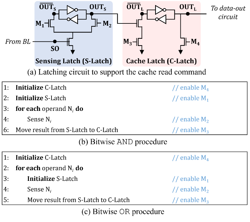
Figures 6(b) and 6(c) describe how ParaBit performs in-flash bitwise AND and OR operations, respectively, by intelligently controlling the latching circuit shown in Figure 6(a).555ParaBit also introduces several mechanisms to support other bitwise operations (e.g., bitwise XOR) and different approaches that exploit the common bit-encoding scheme for MLC NAND flash memory, but we discuss only AND and OR since the others have key drawbacks, such as costly additional inverter logic at each BL to support bitwise XOR operations. Bitwise AND in ParaBit. To perform a bitwise AND operation, ParaBit serially reads operands sharing the same bitline (lines 3 and 4 in Figure 6(b)) while neither enabling M nor re-initializing the sensing latch. Doing so allows ParaBit to keep the result of the bitwise AND of the serially read operands in the sensing latch (node OUT). If the read cell stores ‘0’ (i.e., if the value at SO is ‘1’), enabling only M causes OUT0 regardless of the current value at node OUT. When the cell stores ‘1’ (i.e., when SO0), sensing the cell does not change the value at node OUT. In other words, sensing new data N leads to OUT1 only if both the new data N and the current value at node OUT are ‘1’, which is equivalent to OUT(N AND OUT). After serially reading all the operands sharing the same bitline (which results in bitwise AND of all the operands at node OUT), ParaBit enables M to move the result from the sensing latch to the cache latch (line 5).
Bitwise OR in ParaBit. To perform a bitwise OR operation, ParaBit also serially reads the operands sharing the same bitline (lines 2 to 5 in Figure 6(c)) as in bitwise AND, but it reinitializes the sensing latch (line 3) before sensing each read and activates M (line 5, i.e., moves the result from the sensing latch to the cache latch) after sensing each operand. Doing so keeps the result of the bitwise OR of the read operands sharing the same bitline in the cache latch (node OUT). If newly read data N in the sensing latch (i.e., OUTN) is ‘1’, enabling M results in OUT1 regardless of the current value of node OUT. When NOUT‘0’, activating M does not change the value at node OUT. Hence, latching new data N to the cache latch causes OUT0 only if both the new data N and the current value of OUT are ‘0’, which is equivalent to OUT(N OR OUT).
Benefits of In-Flash Processing. Figure 7 shows an example where ParaBit-like in-flash processing (IFP) can provide benefits over conventional outside-storage processing (OSP) and in-storage processing (ISP) that process data using compute units in the host CPU/GPU and inside the SSD, respectively. Figure 7(a) depicts the target SSD considered in this example. The SSD has eight channels, each of which is shared by four 2-plane dies (i.e., 64 planes in total) with 16-KiB pages. We assume a page-read latency (tR) of 60 µs, a channel bandwidth of 1.2 GB/s between a channel and the SSD controller [109], and an external I/O bandwidth of 8 GB/s (4-lane PCIe Gen4) between the host and the SSD. Figures 7(b), 7(c) and 7(d) show the execution timeline for a channel when an application uses one of OSP, ISP, and IFP, respectively, to perform bulk bitwise OR operations on three 1-MiB bit vectors A, B, and C (i.e., A OR B OR C). We assume that each bit-vector is distributed across all the 64 planes in the SSD as shown in Figure 7(a).
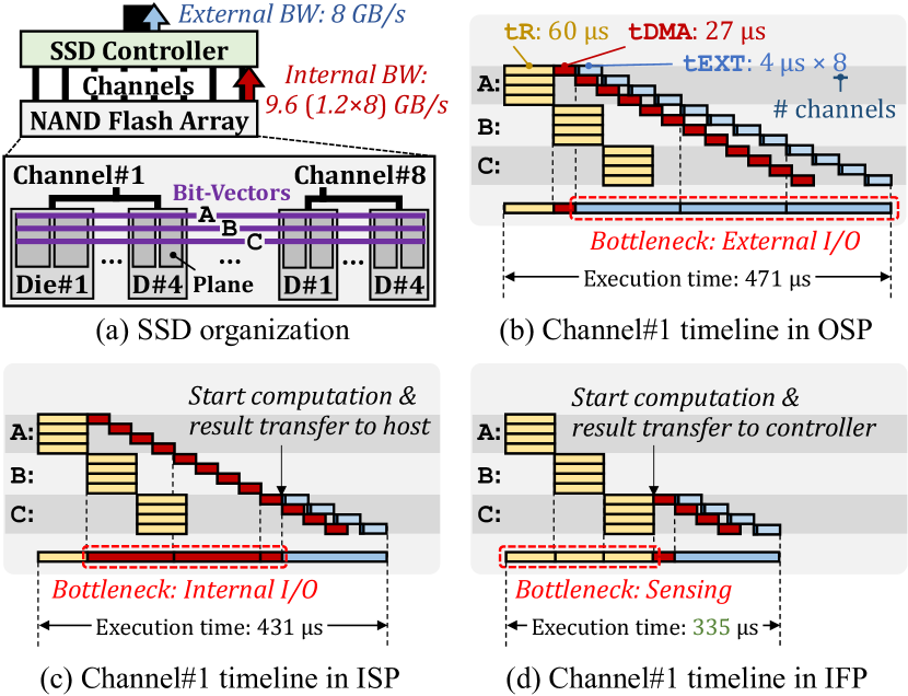
Figure 7(b) shows the execution timeline of bulk bitwise operations for one of the eight channels in OSP. To achieve the highest possible performance using OSP, the host must perform concurrent multi-plane reads across the NAND flash dies for each operand. The operands themselves are read sequentially (tR for operands A, B and C in Figure 7(b)). Once an operand is read to the sensing latch, it can be transferred to the SSD controller (tDMA) and subsequently to the host (tEXT) while a read is simultaneously being performed on the next operand. Given the flash channel and external I/O bandwidth, each die requires tDMA27 µs and tEXT4 µs to transfer 32-KiB data (2 planes16-KiB page) to the SSD controller and to the host, respectively. While tEXT per die is lower than tR and tDMA, the data movement between the host and the SSD (called External I/O in Figure 7(b)) bottlenecks performance, as the SSD serially transfers all the bit vectors from the eight channels through the external I/O interface for computation in the host CPU.
Figure 7(c) shows the execution timeline of a channel in the ISP approach. ISP can use per-channel accelerators (e.g., [50, 55, 110, 56, 16]) to reduce external data movement by performing computation in the SSD controller and transferring only the computation result to the host system. However, the SSD-internal data movement between the SSD controller and NAND flash dies (called Internal I/O in Figure 7(c)) becomes the new performance and energy bottleneck in ISP. This is because the internal data movement must be serialized through the channel shared by the NAND flash dies, while the dies connected to the channel can concurrently perform page reads.
Figure 7(d) shows the execution timeline of a channel for the state-of-the-art IFP approach, ParaBit. ParaBit can effectively reduce both internal and external data movement by performing the computation as the operands are read within the NAND flash chips and transferring only the computation result to the SSD controller and the host, thereby significantly improving performance and energy efficiency. In state-of-the-art IFP, internal data movement between the SSD controller and the NAND flash dies is not a bottleneck, but sensing the data becomes a bottleneck, as Figure 7(d) shows.
3.2 Limitations of State-of-the-Art
We identify two key limitations of ParaBit, the state-of-the-art IFP technique for bulk bitwise operations.
Unexploited Potential of IFP Capabilities. Despite ParaBit’s benefits over other processing approaches, we identify that ParaBit still misses a large potential of exploiting IFP to significantly improve the performance and energy efficiency of bulk bitwise operations. As explained in Section 3.1, ParaBit serially reads every operand from a bitline (tR in Figure 7(d)). Each read of an operand requires a costly (i.e., slow) sensing operation in ParaBit. Such serial reading of every operand poses a big bottleneck when operations need to be performed across more than two operands. We identify that NAND flash memory has inherent capability to perform bulk bitwise operations on a large number of operands (i.e., tens) at once (i.e., using only a single sensing operation) due to (i) its unique cell-array structure and (ii) flash cells’ operation principles. First, as explained in Section 2.1, in NAND flash memory, several tens or more than a hundred of flash cells are serially connected (as in digital NAND gates), and thousands of NAND strings are connected to a single BL (as in digital NOR gates). Second, a flash cell is similar to a normal MOS transistor, a basic component for digital logic gates, in its structure and operation principles. These observations lead us to develop a new IFP technique (described in Section 4) that does not have the sensing bottleneck that the state-of-the-art has: our new technique performs bulk bitwise operations on multiple operands with only a single sensing operation.
Limited Applicability. ParaBit’s applicability is limited to highly error-tolerant applications because it is not designed to take into account the highly error-prone nature of NAND flash memory. As explained in Section 2.2, due to the error-prone nature of NAND flash memory, using ECC and data randomization is essential to guaranteeing the reliability of stored data. However, ParaBit cannot leverage any of the widely-used ECC and randomization techniques, as it performs bulk bitwise operations while reading the operands. Bitwise AND or OR operations on ECC-encoded or randomized data lead can easily lead to incorrect results during ECC decoding or de-randomization. While storing fewer bits per cell can reduce RBER compared to advanced MLC techniques (e.g., triple-level cell (TLC) or quad-level cell (QLC) techniques), ParaBit can be used only when the application can tolerate the NAND flash chips’ RBER (pre-correction error rate), which is still very large as reported in prior works [67, 71, 69, 73].
To better understand the impact of NAND flash reliability on the applicability of IFP, we perform real-device characterization using 160 TLC NAND flash chips (see Section 5.1 for more detail on our methodology). Figure 8 shows the average RBER across 3,686,400 WLs randomly selected from 160 NAND flash chips we analyze. We measure each WL’s RBER (without applying ECC) when (i) programming it in (a) SLC mode and (b) MLC mode and (ii) enabling (left) and disabling (right) data randomization under different P/E-cycle counts (PEC) and retention ages.
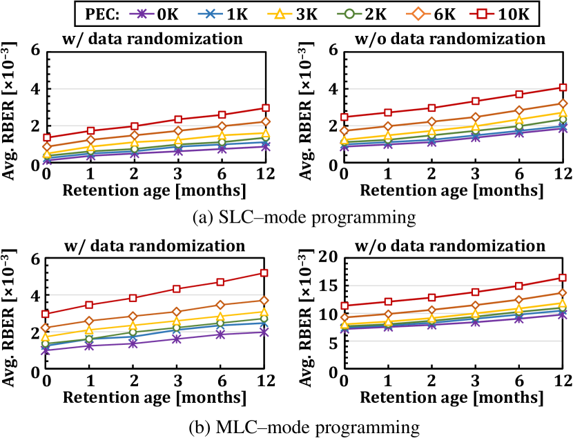
We make three key observations. First, even when using SLC-mode programming with data randomization (left plot in Figure 8(a)), the average RBER is significantly (i.e., around 12 orders of magnitude) higher than the uncorrectable bit-error rate (UBER) requirement of an SSD (e.g., to [111, 112, 67, 73, 71, 69]). Second, disabling data randomization (right plots in Figures 8(a) and 8(b)) significantly increases the RBER of stored data by 1.91 and 4.92 in SLC mode and MLC mode, respectively. Third, as expected, using MLC-mode programming (plots in Figure 8(b)) significantly degrades the reliability of stored data, leading to up to 4 the RBER of SLC-mode programming. Based on our observations, we conclude that the state-of-the-art IFP technique is hard to adopt for applications that cannot tolerate a bit error rate range of 8.6 to 1.6 (the RBER range across the two plots in Figure 8(b)), which is very large.
Our goal in this work is to develop a new in-flash processing technique that (i) maximizes performance and energy efficiency by fully exploiting the inherent computation capability of NAND flash memory to enable many-operand computation with a single sensing operation and (ii) provides high data reliability (i.e., zero bit errors in computation results) so that it is applicable to a wide range of error-intolerant applications.
4 Flash-Cosmos: Key Mechanisms
We present the two key ideas of Flash-Cosmos (Flash Computation with One-Shot Multi-Operand Sensing) that overcome the limitations of the state-of-the-art.
4.1 Multi-Wordline Sensing (MWS)
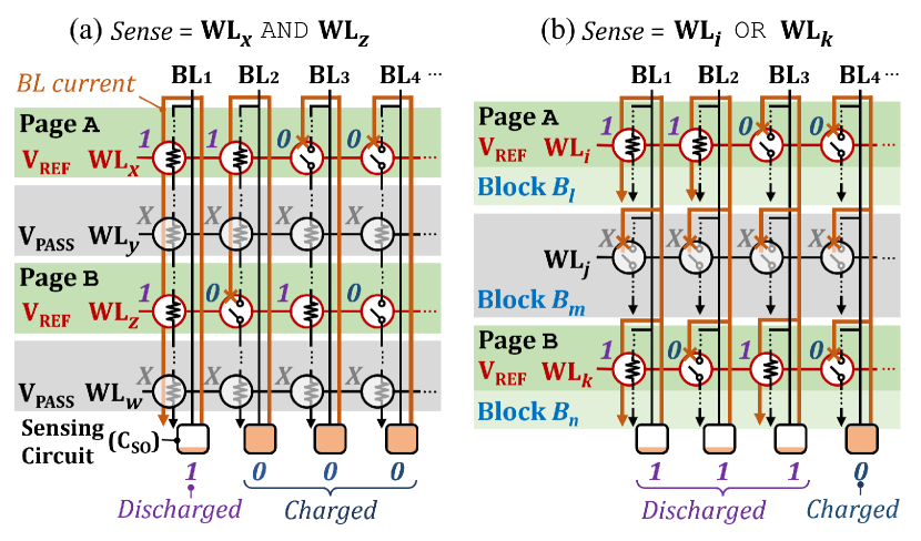
Key Idea. MWS is based on our key observation that simultaneously reading multiple WLs in NAND flash memory results in bitwise AND or OR of the WLs. Figure 9 shows how MWS enables a NAND flash chip to perform bulk bitwise (a) AND and (b) OR operations on two operands with a single sensing operation. While Figure 9 shows bulk bitwise operations on only two operands, Flash-Cosmos can support multi-operand bulk bitwise operations (on tens of operands). For bitwise AND, the NAND flash chip simultaneously applies V to multiple target WLs that contain the source operands of the bulk bitwise operation (WLx and WLz in Figure 9(a)) within a block, which we call intra-block MWS.666Intra-block MWS, which applies V to two or more WLs, differs from a regular read operation that applies V only to a single WL. ParaBit [21], the prior state-of-the-art IFP technique, uses regular read operations. If the chip applies V to all non-target WLs (e.g., WLy and WLw) as in a regular read, a BL can be sensed as discharged only when all the target cells in the corresponding NAND string are erased (i.e., VV). In other words, the sensing circuitry would read a BL as ‘1’ only if all the target cells store ‘1’ (BL1 in Figure 9(a)) and it would read a BL as ‘0’ if any of the target cells stores ‘0’ (BL2, BL3, BL4 in Figure 9(a)), which is equivalent to the bitwise AND operation. The intra-block MWS operation can easily be generalized to more than two operands by applying V to more than two wordlines, leading to the computation of the bitwise AND of all such wordlines with a single sensing operation. For bitwise OR, we introduce inter-block MWS, where the chip simultaneously applies V to multiple WLs (WLi and WLk in Figure 9(b)) of different blocks while applying V to all non-target WLs in those blocks. Doing so causes a BL to be discharged if at least one of the target cells in the corresponding NAND string is erased. In other words, the sensing circuitry would read a BL as ‘0’ only if all the target cells in the BL store ‘0’ (BL4 in Figure 9(b)) and it would read a BL as ‘1’ if any of the target cells stores ‘1’(BL1, BL2, BL3 in Figure 9(b)), which is equivalent to the bitwise OR operation. The inter-block MWS operation can easily be generalized to more than two operands by applying V to more than two wordlines, each in a different block, leading to the computation of the bitwise OR of all such wordlines across different blocks with a single sensing operation.
As mentioned above, both types of MWS are capable of single-sensing bulk bitwise operations even for more than two operands. This property enables MWS to be more powerful than prior NDP proposals that leverage multi-wordline (or multi-row) activation for in-memory computation in two aspects. First, although prior works also propose to activate multiple wordlines to perform bulk bitwise operations inside various memory devices [37, 7, 20, 57, 8], the number of source operands that can be computed on at the same time is limited (usually to only two), thereby requiring sequential sensing of more operands like ParaBit.777Exceptionally, Pinatubo [20] can perform the bitwise OR operation on a large number of rows with a single sensing operation. However, Pinatubo cannot support the bitwise AND operation for more than two operands. Second, there exist several proposals that leverage multi-wordline activation to perform accumulative computation (e.g., multiply-accumulate operations) inside NAND flash memory [57, 58, 59, 60, 61, 62, 63], but they rely on analog current sensing, which requires significant changes to regular flash chips (for instance, in a system with multiple memristor-based crossbar arrays, the addition of a precise analog-to-digital converter (ADC) to each array is costly (e.g., each ADC accounts for 58% of the chip power and 31% of the chip area even when each ADC is shared across 128 output columns [113])).
Intra- and inter-block MWS can be combined to perform complex bitwise AND and OR operations.888Section 6.1 explains how Flash-Cosmos supports other common bitwise operations (e.g., NOT, NAND, NOR, XOR, and XNOR). Suppose that blocks Blkl and Blkn in Figure 9(b) have pages (WLs), each of which stores bit vectors Ai and Bi (1), respectively. If we simultaneously apply V to all the WLs in the two blocks, the chip would read a BLj as ‘1’, only when at least one of Blkl and Blkn has a NAND string in which every cell stores ‘1’, which is equivalent to:
| (1) |
Feasibility & Overhead. Applying MWS to commodity NAND flash chips is highly feasible at low cost. In fact, existing chips already use/support both inter- and intra-block MWS for other purposes. For example, after erasing a block, a NAND flash chip needs to check if all the cells in the block are completely erased (called erase verify) by simultaneously applying V to all the cells [92], i.e., the chip performs intra-block MWS for all WLs in the block. Also, manufacturers commonly design a chip to support the activation of multiple WLs (i.e., intra-block MWS) and multiple blocks (i.e., inter-block MWS), to perform multi-page reads/writes and multi-block erases that are critical for rapid testing of the chip [92].
The MWS scheme has two potential drawbacks. First, an inter-block MWS would consume more power compared to a regular page read since it needs to activate more blocks, which requires charging of all the WLs in multiple blocks. Note that an intra-block MWS operation’s power consumption is lower compared to a regular read because it applies V to additional target WLs, to which a regular read would apply V (which is several times larger than V). Second, the latency for a reliable MWS operation may be longer than the default read latency tR since the target data of an MWS operation is programmed without randomization using the ESP scheme (explained in Section 4.2). Without randomization, a NAND string can have low resistance (e.g., when all the cells are in the erased state) compared to with randomization (where around 50% of the cells are always erased), which may increase the precharge latency and the evaluation latency (see Figure 2) for reliable operation. We evaluate the potential drawbacks in Section 5.
4.2 Enhanced SLC-Mode Programming (ESP)
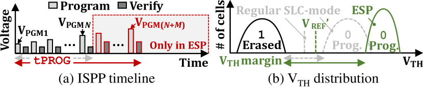
Key Idea. ESP enhances existing SLC-mode programming by maximizing the margin between the two V states. Figure 10 shows how ESP improves reliability compared to regular SLC-mode programming. NAND flash memory commonly uses the incremental step pulse programming (ISPP) scheme [114, 79] to precisely control the threshold voltage (V) of a NAND flash cell and to narrow the width of V state distributions. As depicted in Figure 10(a), the ISPP scheme gradually increases the program voltage from V with a certain step voltage (V), until the V level of every cell in the WL reaches its target voltage V. At the end of each ISPP step, the chip checks if each cell’s V level has reached its V (i.e., Verify in Figure 10(a)), and excludes such cells from the next ISPP step. The key idea of ESP is to perform additional ISPP steps (after performing regular SLC-mode programming), using (i) an increased V value (for each cell), which further moves the programmed V state to a higher voltage level, and (ii) a decreased V value, which narrows the width of the programmed V state distribution. Doing so significantly increases the margins from the new read-reference voltage (V’) to both the erased and the programmed V states, as shown in Figure 10(b), which makes the cells less vulnerable to many error sources present in NAND flash memory [67].
Feasibility & Overhead. Applying ESP to commodity NAND flash chips is highly feasible at low cost due to two reasons. First, modern MLC NAND flash memory commonly supports SLC-mode programming for several reasons, e.g., storing reliability-sensitive data [78], managing an SLC write buffer [77] or using unreliable cells for data storage in case they cannot be used in MLC mode [115]. Second, commodity NAND flash chips can tune ISPP parameters [79, 80, 81, 82, 83, 84] using the SET FEATURE command [116, 64], which is essential to post-fabrication optimization of NAND flash chips. The SET FEATURE command is also used to dynamically adapt to changes in P/E cycles [65, 67] and reliability characteristics of NAND flash cells [65, 67].
ESP has two drawbacks. First, it increases the program latency by performing additional ISPP steps. Second, because it uses SLC-mode programming, it requires double the WLs to store the same amount of data compared to MLC-mode programming. We provide a detailed analysis of the performance and capacity overheads of ESP in Section 8.3.
![[Uncaptioned image]](/html/2209.05566/assets/x11.png)
5 Real Device Characterization
This section presents our characterization of 160 real 3D NAND flash chips to validate the feasibility, performance, and reliability of the two key mechanisms of Flash-Cosmos.
5.1 Characterization Methodology
Infrastructure. We use an FPGA-based testing platform that contains a custom NAND flash controller and a temperature controller. The flash controller supports all the commands implemented in our NAND flash chips, including not only basic read/program/erase commands but also various test-mode commands necessary to dynamically change operating parameters (e.g., the ISPP step voltage and other timing parameters) and simultaneously activate multiple WLs. The temperature controller maintains a NAND flash chip within ±1∘C of the target temperature. This feature allows us to (i) test all the chips under the same operating temperature (85∘C) and (ii) accelerate retention loss based on Arrhenius’s Law [117], which is essential to real device characterization under long retention ages (e.g., 1 year) while maintaining reasonable testing time. We characterize 160 48-layer 3D TLC NAND flash chips, where a NAND string consists of 48 flash cells and the page size is 16 KiB. Under regular SLC-mode programming, the chips have a read latency tR22.5 µs and a program latency tPROG200 µs.
Methodology. To minimize the potential inaccuracies in our characterization results, we carefully design our experiments following the JEDEC standards [118, 119] that specify the test methodology recommended for evaluating the reliability of commercial-grade NAND flash products. To ensure high-confidence reliability tests, JEDEC recommends testing more than 39 flash chips from three different wafers. Our 160 flash chips are fabricated from five different wafers, and we select 120 blocks (not sub-blocks) from each of the 160 chips at random locations. We test every page in each selected block (a total of 3,686,400 WLs) to obtain statistically significant results.
To evaluate Flash-Cosmos’ reliability under the worst-case operating conditions, we measure each WL’s RBER under a 1-year retention age at 30∘C [112] and 10K P/E cycles.999In our RBER measurements, we exclude faulty cells that introduce permanent (non-transient) errors due to defects in fabrication since (i) faulty cells can be profiled and excluded for the purpose of Flash-Cosmos, and (ii) manufacturers can significantly reduce the faulty-cell fraction by specially designing chips for Flash-Cosmos at the cost of yield and/or technology node size. We increase a block’s P/E-cycle count by repeating the cycle of programming every page in the block (in TLC mode) and erasing the entire block. Unless specified otherwise, we program each page using the checkered data pattern, the worst-case data pattern for NAND flash reliability where any two adjacent cells (both horizontally and vertically) are programmed either to the highest V state (e.g., the P7 state in TLC mode) or to the lowest V state (i.e., the Erased state).
5.2 Characterization Results
ESP Latency & Reliability. We first study the trade-off between the reliability and program latency of the ESP scheme. Figure 14 shows the average RBER per 1-KiB data when we program the WLs while increasing the ESP latency tESP for more precise ISPP control. We plot the RBER of the worst, median, and best block out of all the tested blocks and normalize the increased tESP values to the default program latency tPROG for regular SLC-mode programming.
We make two key observations from Figure 14. First, it is possible to avoid raw bit errors without data randomization by enhancing SLC-mode programming, at the cost of an increase in program latency.101010We also tried to achieve the same level of RBER by enhancing MLC-mode programming, but the RBER of MLC-mode programming does not decrease below 10-4 even when we increase the program latency to 5 ms. When we increase tESP by more than 90% compared to tPROG, we observe zero bit errors in our tested pages that contain more than 4.831011 bits in total, which means that the statistical RBER of ESP is lower than 2.07×10-12.111111The result is not enough to guarantee the JEDEC-specified UBER requirements (see Section 5.1), but we carefully select the evaluated blocks to avoid any potential inaccuracy in our results. Given the limitations in academia, it is challenging to experimentally guarantee the UBER requirements, which requires around 1,000 samples and 1,000 longer testing time than our experiments using our experimental testing infrastructure. Second, the ESP scheme’s reliability improvement significantly increases with tESP. For the median block, increasing tESP by 60% achieves an order of magnitude RBER reduction. We conclude that the ESP scheme is essential for achieving effectively zero bit errors in the computation results of in-flash processing and thus ESP can increase applicability of in-flash processing to a much wider range of applications.
MWS Latency & Reliability. We measure tMWS, the minimum latency for an MWS operation to achieve zero bit errors in all the tested blocks. First, we perform intra-block MWS operations while changing the number of read WLs from 1 to 48 (the number of WLs in a NAND string). Second, we perform inter-block MWS operations on all WLs in the target blocks while changing the number of activated (target) blocks from 1 to 32. In both experiments, we first increase a target block’s P/E cycle count using a checkered data pattern. Next, we check the correctness of intra-block MWS under high disturbance and noise, induced by programming the block using a different data pattern. This new data pattern maximizes the resistance of NAND strings in the block by programming the block to meet two conditions; (i) the number of cells that store bit value ‘1’ (i.e., ‘1’ cells) must be less than two; (ii) if a NAND string has a ‘1’ cell, the cell must be in one of the MWS operations’ target wordlines. As explained in Section 4.1, bypassing data randomization can affect the read latency (both tR and tMWS) for reliable operation by decreasing a NAND string’s resistance compared to the typical read of randomized data. We validate the correctness of MWS by comparing the result of MWS operations that we obtain from the real chips to the correct results of the bitwise operations on the stored data.
Figures 14 and 14 show the tMWS value (as a multiple of tR) for intra- and inter-block MWS operations, respectively. We make three key observations from the results. First, bypassing data randomization does not increase a regular read operation’s latency. As shown in Figure 14, using the default read latency introduces no error when we read only a single WL in a block. Second, intra-block MWS does not significantly increase the read latency. Even when we simultaneously read all the 48 WLs in a block, tMWS is only 3.3% higher than tR. When we perform intra-block MWS on eight (or fewer) WLs, tMWS is less than 1% higher than tR. Third, although inter-block MWS (shown in Figure 14) affects tMWS more significantly compared to intra-block MWS, it can still provide significant benefits over individual reads of the same WLs. As shown in Figure 14, when simultaneously reading WLs in 32 different blocks, tMWS is 36.3% higher than tR. This is because activating multiple blocks significantly increases the number of WLs to precharge at the same time. The increased WL-precharge time is mostly hidden by the BL-precharge time until we activate eight blocks, but it becomes larger than the BL-precharge time as the number of activated blocks further increases, which causes the latency of a reliable MWS operation to be longer than the latency of a regular page read. However, the increased latency of MWS on 32 WLs (1.363tR) is much lower than the latency to individually (serially) read 32 WLs (32tR).
Based on our observations, we draw three major conclusions. First, we demonstrate that real commodity NAND flash chips can reliably support both intra-block and inter-block MWS operations, so computer architects can build a system that leverages Flash-Cosmos, as long as they have access to the command interfaces used for our characterization. Second, both types of MWS significantly accelerate in-flash bulk bitwise operations in commodity NAND flash chips at low cost. Third, it is possible to support both types of MWS with a small latency increase over the default read latency. If we limit the maximum number of simultaneously-activated blocks for inter-block MWS to 4, we can support any MWS operation with a fixed latency (tMWS) only 3.3% higher than tR.
Maximum Power Consumption of Inter-Block MWS. As explained in Section 4.1, inter-block MWS consumes more power compared to a regular page read due to the higher number of activated WLs at the same time. Understanding the impact of MWS on power consumption is important because a NAND flash-based SSD has a limited power budget (e.g., 75W for PCIe Gen4 SSDs [120]). Figure 14 shows the average power consumption of a NAND flash chip when we perform inter-block MWS as a function of the number of simultaneously-activated blocks. To measure the worst-case power consumption, we read only one WL per each block (i.e., we apply V to only one WL per block while applying V (V) to all non-target WLs). We normalized all values in Figure 14 to the average power consumption of a regular page-read operation.
We make three observations. First, the power consumption of a NAND flash chip considerably increases with the number of activated blocks for inter-block MWS. Increasing the number of activated blocks from one to two increases the average power consumption by about 34%. Second, despite the non-trivial increase in power consumption, it is possible to support inter-block MWS within the SSD’s power budget. Until we activate four blocks, the power consumption of inter-block MWS remains lower than that of an erase operation. Third, inter-block MWS is more energy efficient compared to serial reads of the same WLs. For example, performing an inter-block MWS operation on four different blocks would cause about 80% power increase compared a regular read, but due to its negligible latency increase (3.3%), it significantly reduces the energy consumption by 53% compared to individual reads of the four WLs. We conclude that, with a proper limit on the number of inter-block MWS, Flash-Cosmos would not require an increase in the power budget of commodity SSDs.
6 Design of Flash-Cosmos
We present our design of Flash-Cosmos to support efficient in-flash bulk bitwise operations.
6.1 Enhanced Computation Capability
We enhance the basic capability of Flash-Cosmos (beyond the bitwise AND and bitwise OR operations introduced in Section 3.1) in two ways.
Supporting Other Bitwise Operations. We design Flash-Cosmos to also support bitwise NOT/NAND/NOR/XOR/XNOR operations by leveraging two existing features that are widely supported in real NAND flash memory chips. First, as explained in Section 2.1, modern NAND flash memory commonly supports inverse reads [85], which enables Flash-Cosmos to perform not only bitwise NOT operations but also bitwise NAND and NOR operations. Flash-Cosmos performs NOT of a WL by simply reading the WL in inverse-read mode. If we perform intra-block (inter-block) MWS while controlling the sensing latch circuit in inverse-read mode, the sensed data would be the inverse value of the bitwise AND (OR) of all the WLs simultaneously read, i.e., bitwise NAND (NOR) by definition.
Second, many modern NAND flash chips (including the 160 chips used in our real-device characterization, Section 5) support a bitwise XOR operation between the data in different latches (i.e., two/three additional latches available in a NAND flash chip for MLC/TLC program operation) [87, 88]. This feature is essential for supporting on-chip randomization [87] and improving testability (e.g., it significantly reduces a NAND flash chip’s test time by enabling comparison of programmed data to a golden value without reading the data out of the chip [121, 122]). By using this feature along with inverse reads, Flash-Cosmos can also support bitwise XNOR operations since
| (2) |
To be specific, Flash-Cosmos uses the existing XOR logic while performing an inverse read for either of the two operands.
Improving the Performance of the Bitwise OR Operation. The performance of bitwise OR using inter-block MWS is limited compared to that achieved by bitwise AND using intra-block MWS. As demonstrated in Section 5.2, commodity NAND flash chips can perform bitwise AND of all the WLs in a block via a single intra-block MWS operation. However, the maximum number of operands in inter-block MWS is limited due to high power consumption.
We can remove this restriction on the maximum number of activated blocks by performing bitwise OR using 1) intra-block MWS along with 2) inverse reads and 3) taking advantage of De Morgan’s laws. If we store operands in a block with their inverse data (instead of the original data), we can perform bitwise OR of the operands with a single intra-block MWS operation by leveraging the inverse read mode and De Morgan’s laws:
| (3) |
Note that (i) Flash-Cosmos can return the original data of such operands via inverse reads (ANOT ), and (ii) inter-block MWS is still useful for combined bitwise AND/OR operations as explained in Section 4.1 (Equation 1).
Increasing Maximum Number of Operands for IFP. Flash-Cosmos alone cannot completely avoid off-chip data transfer for bitwise AND/OR/NAND/NOR operations if the number of operands exceeds the number of WLs in a block. This is because intra-block MWS involves a single sensing operation to read all WLs within a block, thereby limiting the maximum number of operands to the number of WLs in a block. Inter-block MWS has a stronger constraint on the maximum number of operands due to the limited power budget as explained in Section 5.2.
Fortunately, Flash-Cosmos can accumulate the results of multiple intra-block MWS operations by leveraging ParaBit, which has fewer constraints on the maximum number of operands. For example, suppose that (i) a block has WLs, and (ii) Flash-Cosmos needs to perform bitwise AND of all WLs of different blocks (i.e., the number of total operands is ). We can accumulate the results in two steps. First, Flash-Cosmos performs bitwise AND on each block for operands at a time. Second, Flash-Cosmos performs bitwise AND on the results from the blocks.
6.2 Flash-Cosmos Command Set
Although we demonstrate that our NAND flash chips already support all necessary features to perform the ESP and MWS operations in their test-mode command set, efficient design of Flash-Cosmos commands is important due to two reasons. First, NAND flash vendors consider their test-mode command set design to be proprietary and do not reveal any details in publicly-accessible documentation. Second, efficient command set design can significantly reduce the necessary changes to the NAND flash chip’s control logic and communication overheads with a flash controller.
Figure 15 shows three new NAND flash commands that we design for Flash-Cosmos: (a) MWS, (b) ESP, and (c) XOR. We design the MWS command to be used for all three necessary features in Flash-Cosmos except for bitwise XOR: (i) intra- and inter-block MWS, (ii) inverse read, and (iii) accumulation of the results of all reads as described in Section 6.1. To this end, we extend the regular read command that contains the operation code and target page address in three aspects. First, we add the ISCM command slot before the address slot to allow a flash controller to turn on/off four features by setting the dedicated flags: (i) inverse-read mode, (ii) sensing-latch (S-latch) initialization, (iii) cache-latch (C-latch) initialization, and (iv) data transfer from S-latch to C-latch. Second, we enable the flash controller to efficiently specify the WLs to activate for MWS operations by sending the page bitmap (PBM) instead of the page index in the address slot. Third, we design an MWS command to have up to four address slots for inter-block MWS by sending the additional block address and PBM after a CONT (continue) slot.121212CONT is a command slot to indicate that an address cycle will follow next. CONF is a command slot to indicate the end of the command sequence. The ESP command has the same command interface as the regular program command, and the XOR command performs bitwise XOR between two (sensing and cache) latches and stores the result in the C-latch.
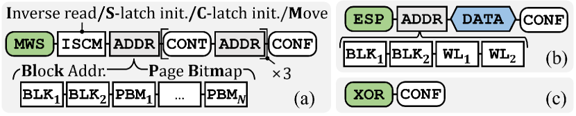
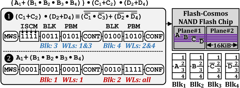
Figure 16 shows how a flash controller can use Flash-Cosmos to perform bulk bitwise operations using an example that makes two assumptions: (i) a Flash-Cosmos-enabled chip stores four sets of four bit vectors, Ai, Bi, Ci, and Di, in four blocks Blki (14), each of which has four pages; (ii) bit vectors Ci and Di are programmed using their inverse data with the knowledge that they would be used for bitwise OR (Section 6.1). Suppose that the user would like to perform the following bitwise operations:
| (4) |
As shown in Figure 16, the user can perform bitwise operations using two intra-block MWS commands, one for while enabling the inverse-read mode and initialization of both latches and the other for while disabling the inverse-read mode and initialization of both latches. By disabling the initialization of both latches while performing the second MWS command, the results of the two MWS commands, and , are accumulated in both the S-latch and the C-latch (Section 6.1). Note that the order of the two MWS commands is important, as an inverse read requires S-latch initialization, which prevents the accumulation of the results.
6.3 System Support
We briefly discuss the end-to-end system support that we envision to efficiently enable Flash-Cosmos.
Requirements. There are two key requirements for a system to take full advantage of Flash-Cosmos-enabled NAND flash chips. First, the target data of bitwise operations needs to be properly stored using ESP. To maximize the performance benefits of Flash-Cosmos, it is important to store as many operands of the target bitwise operation as possible in the same block, which minimizes the number of MWS operations required. For example, bitwise OR on 48 pages (i.e., operands) would require 12 inter-block MWS operations if each operand is stored in different blocks, assuming that the maximum number of pages for inter-block MWS is limited to 4 in order to avoid maximum power consumption related issues. However, when the operands are stored in the same block with their inverse data, it is possible to perform the same bitwise OR operation with a single intra-block MWS operation using inverse-mode read (Section 6.1). Second, the host system needs to interact with the underlying SSD in order to efficiently store the data to maximize the benefits of Flash-Cosmos.
Application Changes. In our design, the application program needs to decide how to store data in three aspects. First, the application determines the data that will be used for bulk bitwise operations so that it can inform the SSD to selectively use ESP for only such data (to minimize the storage overhead due to SLC mode). Second, depending on the computation that can benefit the most from Flash-Cosmos, the application decides whether or not to store the inverse of the original data. For example, if the application performs bitwise OR more frequently than bitwise AND for certain data, it could be more beneficial to store the inverse data to leverage intra-block MWS for bitwise OR as well. Third, the application decides which operands to be stored in the same block to minimize the number of MWS operations required for the same bitwise operation.
System Software Changes. In our design, the application program interacts with the SSD using the Flash-Cosmos library that includes two methods: (i) fc_write, which writes the operand data for bitwise operations, and (ii) fc_read, which reads the results of bitwise operations. Using fc_write, the application informs the SSD of the context of the operation, such as the programming mode and the location (e.g., logical block address), to ensure that the data is properly stored for in-flash computation. To perform an in-flash bitwise operation, the application uses fc_read to specify to the SSD the locations of the target operands, the size of the operands, and the types of bitwise operations required.
SSD Changes. In our design, the SSD firmware requires two key changes. First, it generates Flash-Cosmos commands to properly handle fc_write and fc_read from the host system. Second, the SSD firmware maintains additional metadata necessary for Flash-Cosmos, such as each page’s programming mode and the location where the page should be stored.
In this work, our focus is on investigating the feasibility and benefits of Flash-Cosmos using modern NAND flash memory chips. While the end-to-end support for Flash-Cosmos requires several changes within layers of the system stack, we believe that existing approaches can be applied to meet the key requirements (e.g., efficient storage layout designs [37, 8, 7, 9], host-SSD communication [9, 50, 78], and metadata management inside the SSD [50, 78]). We leave more efficient end-to-end system designs and software stack for Flash-Cosmos to future work.
7 Methodology
Evaluated Systems. To evaluate the effectiveness of Flash-Cosmos, we analyze four computing platforms: (i) an outside-storage processing system (OSP),(ii) an in-storage processing system (ISP), (iii) ParaBit (PB) [21], and (iv) Flash-Cosmos (FC). OSP performs bulk bitwise operations using the host CPU concurrently with reading the operands from the SSD to main memory in batches. ISP leverages an in-storage hardware accelerator that consists of simple bitwise logic and 256-KiB SRAM buffer in order to perform bulk bitwise operations inside the SSD and sends only the final results to the host. PB and FC perform bulk bitwise operations inside the NAND flash chips via the in-flash processing mechanisms described in Section 3.1 and Section 6, respectively, and send only the final results to the host. Unless otherwise specified, we set all the evaluated systems to program (and thus read) the inputs and outputs of bitwise operations in SLC mode for fair performance comparison.
Performance Modeling. We use two state-of-the-art simulators to analyze the performance of the evaluated systems. We model DRAM timing with the DDR4 interface [123] in Ramulator [124, 125], a widely-used cycle-accurate DRAM simulator. We model SSD performance using MQSim [126, 127], a state-of-the-art SSD simulator. We extend MQSim to faithfully model the performance of ISP, ParaBit, and Flash-Cosmos with the timing parameters we obtain from our real-device characterization (Section 5). We model the end-to-end throughput of the evaluated systems based on the throughput of each of two computation stages, SSD read (including in-storage processing in ISP, PB, and FC) and host computation (which we measure on a real host system). Table 1 summarizes the configurations of the SSD and host system used for our evaluation.
| Real Host System | CPU: Intel Rocket Lake i7 11700K [91]; |
|---|---|
| x86 [128]; 8 cores; out-of-order; 3.6 GHz; | |
| Main Memory: 64 GB; DDR4-3600; 4 channels; | |
| Simulated SSD | 48-WL-layer 3D TLC NAND flash-based SSD; 2 TB; |
| Bandwidth: 8-GB/s external I/O bandwidth (4-lane PCIe Gen4); | |
| 1.2-GB/s Channel IO rate; | |
| NAND Config: 8 channels; 8 dies/channel; 2 planes/dies; | |
| 2,048 blocks/plane; 196 (448) WLs/block; 16 KiB/page; | |
| Latencies: tR (SLC mode): 22.5 µs; tMWS: 25 µs (Max. 4 blocks); | |
| tPROG (SLC/MLC/TLC mode): 200/500/700 µs; tESP: 400 µs; | |
| Power: HW Accelerator (only in ISP): 93 pJ for 64B operation; |
Energy Modeling. We measure the energy consumption for host computation using Intel RAPL [129] To model DRAM energy consumption, We use DRAM power values based on the DDR4 model [130, 131]. To model SSD energy consumption, we use the SSD power values of Samsung 980 Pro SSDs [132] and the NAND flash power values that we measure in our real-device characterization (Section 5).
Workloads. We evaluate three real-world applications that heavily rely on bulk bitwise operations. For fair comparison with ParaBit, we evaluate two of the three applications studied in [21], bitmap indices and image segmentation,131313We do not evaluate the other application evaluated in ParaBit [21], image encryption [30], as it relies only on bitwise XOR operations that commodity NAND flash chips already support (see Section 3), i.e., neither ParaBit nor Flash-Cosmos is necessary to perform in-flash processing for such XOR operations. as well as a graph-processing workload called k-clique star listing [19, 133, 134]. For all workloads, we assume that the data set is initially stored in the SSD due to its large size.
1) Bitmap Index (BMI): Bitmap indices [1] are an alternative to traditional B-tree indices for databases, which can provide high space efficiency and high performance for many queries (e.g., join and scan) compared to B-trees. We assume a database that tracks the log-in activities of users for a website every day. For the -th day, the database maintains a vector with elements, each of which is a 1-bit flag to indicate each user’s log-in activity on the day (0: not logged-in, 1: logged-in). Our BMI workload runs the following query: “How many users were active every day for the past months?” Executing the query requires (i) bitwise AND operations on vectors, where is the number of days in the past months, and (ii) a bit-count operation, i.e., an operation that counts the number of ‘1’ (logged-in) bits in a given result vector . We assume a database that tracks the log-in activities of 800 million users and evaluate the BMI workload while varying from 1 to 36. For executing the BMI workload, PB and FC perform the bit-count operation using the host CPU concurrently with sending the result vector to main memory in batches.
2) Image Segmentation (IMS): Image segmentation [135] is an image processing kernel that aims to break an image into multiple regions depending on a given set of colors. To determine whether a pixel belongs to a certain color , our IMS workload uses the YUV color recognition and performs a bitwise AND operation of , where , , and are binary values that can be obtained from pre-processing [135]. In our evaluation, IMS segments images, each of which consists of 800600 pixels, with four colors. This can be done by performing a bulk bitwise AND operation to three bit vectors where each bit-vector contains bits. We assume the three bit-vectors are initially stored in the SSD and evaluate the IMS workload while varying from 10,000 to 200,000.
3) -Clique Star Listing (KCS): -clique star listing [19, 133, 134] aims to find all the -clique stars in an input graph. For a given graph, a -clique is a sub-graph with vertices that are fully connected to each other. A -clique star is a collection of (i) a -clique and (ii) all the vertices in the remainder of the graph that are connected to all vertices of the -clique. Prior work demonstrates that -clique star listing can be significantly accelerated via processing-in-memory with a set-centric formulation [19]. In our evaluation, each vertex is represented using a bit-vector that contains adjacency information to all other vertices in the graph. Each -clique is represented with another bit vector that specifies the set of vertices that belong to the -clique. With such bit-vector representations, our KCS workload can determine a -clique star by performing only a bitwise AND operation of the bit-vectors of all the vertices in the corresponding -clique. To form the final representation of a -clique star, KCS performs a bitwise OR operation of the calculated intermediate bit vector and the bit-vector that represents the -clique. Note that Flash-Cosmos can perform both of the bitwise AND and OR operations simultaneously if the -clique bit vector is stored in a block that is different from than the block that stores the vertex adjacency vectors. We use an input graph with 32 million vertices and 1,024 -cliques and we sweep the dimensions of the cliques, from 8 to 64.
Applications using bulk bitwise operations with many operands can be particularly sensitive to the RBER of NAND flash memory. For example, a single bit error in any of the operands in the BMI workload results in an active user not being counted. The probability of miscounting active users grows as the number of operands increases and rapidly becomes impractical without a sufficiently low RBER. Assuming a best-case RBER of (based on our analysis) and =36, the probability of a correct output is 0.42 which is not acceptable. KCS is similarly error-intolerant due to the large number of operands it uses. In contrast, IMS is more error tolerant due to the fewer operands in this workload. Thus, we expect that Flash-Cosmos would be a good fit for all these workloads, especially BMI and KCS, due to its zero bit error rate in computation results.
8 Evaluation Results
We evaluate the performance and energy efficiency of Flash-Cosmos by comparing its execution time and energy consumption to three baseline computing platforms.
8.1 Impact on Performance
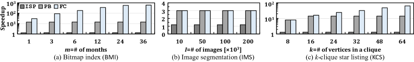
Figure 17 shows the speedups of Flash-Cosmos (FC), ParaBit (PB), and the in-storage processing system (ISP) over the conventional outside-storage processing system (OSP). We make six observations from Figure 17.
First, FC significantly outperforms OSP, providing 32 speedup on average across all three workloads and input data sets. In OSP, computation can be completely hidden by reading of the operands due to the simple nature of bitwise operations, but the SSD’s external bandwidth bottlenecks performance. This means that, when the operands are stored in the storage system, any other outside-storage processing platform (e.g., GPU or near-memory processor) cannot improve the performance of bulk bitwise operations over OSP (unless one increases SSD’s external bandwidth).
Second, FC also significantly outperforms ISP, providing 25 speedup on average. While ISP provides considerable speedup (28%) over OSP by reducing external data movement from the SSD (external bandwidth is 8 GB/s, Table 1), the limited internal SSD bandwidth (9.6 GB/s, Table 1) becomes a new bottleneck. ISP needs to read out all operands from NAND flash chips to the hardware accelerators, which can be largely avoided by in-flash processing.
Third, FC provides large performance improvement over ParaBit. While PB also significantly outperforms OSP (and ISP) by 9.4 (7.2), FC outperforms PB by 3.5 on average across all three workloads and input data sets. This highlights the key benefit of performing MWS in real-world applications.
Fourth, the benefits of FC increase with the number of operands used in bulk bitwise operations. The speedups of FC for BMI are higher compared to the other two workloads, since BMI has a larger number of operands (from 30 to 1,095). In contrast, the performance of PB does not improve as the number of operands increases (e.g., for 16 in KCS). This is because the performance bottleneck of PB shifts to the serial sensing of the operands as discussed in Section 3.2, due to which the latency also linearly increases with the number of operands. As a result, while FC significantly improves performance over OSP/ISP for BMI by 198.4/150.5, PB’s benefits over OSP/ISP for BMI remain at only 14/.
Fifth, the benefits of FC are affected by not only the number of operands but also the operand size. For example, FC does the same operation (AND) over 30 operands for BMI (when =1) and over 32 operands for KCS (when =32). Although KCS has more operands than BMI, we observe that FC provides higher improvement over PB for BMI. This is because the total size of the result bit vectors is smaller in BMI (100 MB) than in KCS (4 GB), which results in reduced external I/O time spent for transferring the results from the SSD to the host. As shown in Figure 7(d), external data movement can become the bottleneck even for in-flash processing if the external I/O time within an application (e.g., due to transferring results out of the SSD) is larger than the overall sensing time. Therefore, the benefit of FC over PB is lower if the external I/O time dominates the overall execution time.
Sixth, FC and PB show almost similar performance for IMS across all input sets. Even though FC reduces the average number of sensing operations by 3 compared to PB when executing the IMS workload, moving the large (up to 44GiB) result vector of IMS to the host dominates the total execution time for both mechanisms. This is in contrast to BMI where the vector size is only 100 MB. Note that, in IMS, both FC and PB provide high speedups compared to ISP and OSP (2.5 and 3, respectively) by reducing the amount of external and internal data transfers, which are the performance bottleneck in IMS.
We conclude that Flash-Cosmos is an effective substrate to accelerate important real-world applications. Flash-Cosmos not only largely outperforms the state-of-the-art IFP technique but also, crucially, provides reliable, error-free execution (which is necessary for correct results in all three real-world workloads we evaluate).
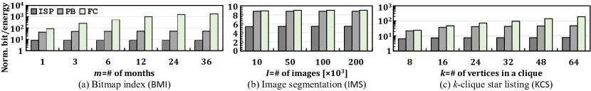
8.2 Impact on Energy Consumption
Fig. 18 shows the energy-efficiency of FC, PB, and ISP , in terms of the number of bits that can be computed/transferred per unit of energy, normalized to that of OSP. We make three observations. First, FC greatly increases energy efficiency over the other evaluated systems, providing 95/13.4/3.3 higher energy-efficiency compared to OSP/ISP/PB, on average across all three workloads and input sets. Flash-Cosmos has the maximum energy savings of 1,839/222/35.5 over OSP/ISP/PB for BMI when =36. Second, the overall trend of FC’s energy-efficiency benefits is similar to its performance benefits. The energy benefits of FC increase (decrease) as the number of operands (the operand size) increases. Third, FC reduces energy by not only reducing data movement but also reducing sensing energy, especially for multi-operand operations. As a result, it provides higher improvements in energy efficiency (95 on average over OSP) than in performance (32 on average over OSP). Note that, as shown in Figures 17(b) and 18(b), for IMS, even though FC performs similarly to PB, it provides 2.3% energy savings. We conclude that Flash-Cosmos is an efficient substrate to eliminate the energy overheads of data movement for many commonly-used real-world applications.
8.3 Overhead Analysis
As briefly discussed in Section 4.2, Flash-Cosmos introduces two key overheads due to the use of ESP for reliable in-flash computation. First, ESP requires 2 the page-program latency compared to regular SLC-mode programming. Second, ESP consumes 2 the storage capacity to store the same amount of data compared to MLC-mode programming.
While the write-performance and capacity overheads are not negligible, we believe that both overheads would not be serious obstacles to the adoption of Flash-Cosmos due to three reasons. First, ESP is essential to ensuring the reliability of in-flash computation.141414In order to be useful for general-purpose computation, ParaBit has to support error-free computation, potentially using ESP. As shown in Section 3.2, regular SLC/MLC-mode programming exhibits significantly higher RBER than the UBER requirement, and ESP effectively solves this important reliability problem that is present in in-flash computation.151515Flash-Cosmos can also work with MLC NAND flash memory while guaranteeing the same level of reliability as ParaBit provides, when the operands are stored in LSB pages. This is because the mechanism of LSB-page reads is the same as SLC-page reads, except for the used read-reference voltage levels (LSB-page read in MLC: V in in Figure 5(b) vs. SLC-page read: V in Figure 5 (a)).
Second, both the write-performance and capacity overheads apply only to the data used for bulk bitwise operations. As such, Flash-Cosmos can minimize these overheads by selectively using ESP only for the data that is involved in in-flash processing (bulk bitwise operations) while programming other data using regular SLC/MLC/TLC-mode programming. Such a functionality is supported by the multiple programming modes in modern NAND flash memory, i.e., any block can be programmed in SLC, MLC, and TLC modes [77, 78, 136].
Third, ESP does not degrade SSD write performance, in terms of both bandwidth and latency, compared to MLC-mode programming. This is because the program latency of ESP (400 µs, Section 4.2) is still lower than the latency of MLC- and TLC-mode programming (500 µs and 700 µs, respectively, in our evaluated chips). We evaluate the sequential write bandwidth of ESP, and the results show that ESP provides a write bandwidth of 4.7 GB/s, which is 73.4%/121.4%/166.7% of the regular SLC/MLC/TLC-mode programming write bandwidth (6.4/3.87/2.82 GB/s).
9 Related Work
To our knowledge, this work is the first to enable in-flash bulk bitwise operations on multiple operands through a single sensing operation, while achieving zero bit errors in the computation results. We already discussed and comprehensively compared to the state-of-the-art technique [21] closely related to Flash-Cosmos (Sections 3, 7 and 8). We briefly describe other NDP proposals at different levels in the memory hierarchy.
In-Flash Processing. Several prior works propose in-flash processing techniques to accelerate the multiply-and-accumulate (MAC) operations in different applications such as neural networks (e.g.,[57, 58, 63, 62, 137, 138, 139, 140, 110]) and mixed signal sensing (e.g.,[60]). Similar to Flash-Cosmos, these mechanisms have high bit-level parallelism, but they exploit analog current accumulation, which requires significant changes to the NAND flash cell array structures, e.g., deploying precise and costly analog-to-digital converters inside the chip (see Section 4.1). In contrast, our mechanism can be adopted in commodity SSDs with very low cost, as we demonstrated in Section 5.
In-Storage Processing. Several prior works propose to leverage the internal processor (e.g., [51, 55, 56, 52, 141, 142, 143, 144, 145, 146, 147, 148, 149, 150, 151, 152, 153, 154]) or embed hardware accelerators (e.g., [49, 50, 155, 156, 157, 158, 159, 16, 160, 161, 15, 17, 162, 163, 164, 165]) within the storage device for computation. Due to their more general-purpose designs, these proposals can perform more diverse and complex operations (e.g., arithmetic operations). However, as discussed in Section 3, in-storage processing needs to first read out the processed data from the flash chips and transmit it to the SSD controller over the SSD-internal I/O link, which is a performance bottleneck. In contrast, Flash-Cosmos can effectively reduce the data movement between NAND flash chips and the SSD controller by performing computation inside the flash chip arrays, leading to more than an order of magnitude higher performance and energy-efficiency than in-storage processing (Section 8).
In-Memory and In-Cache Processing. A large body of prior work proposes various NDP techniques at other levels of the memory hierarchy, e.g., in main memory (e.g., [7, 8, 39, 20, 166, 54, 167, 168, 169, 170, 6, 171, 172, 38, 9, 173, 174, 175, 176, 177, 178, 14, 179, 180, 181, 182, 183, 184, 185, 186, 187, 188, 189, 190, 191, 192]) and in SRAM caches (e.g., [37, 40, 193, 194, 41, 195, 196, 197, 198, 199]). Even though these works provide significantly lower access latency and high reliability, once the size of the processed data exceeds the cache and main memory capacity, the data needs to move between the storage devices and the rest of the memory hierarchy. Flash-Cosmos can complement these NDP approaches (including in-storage processing) by processing large amounts of data inside flash arrays and communicating only the results of the computation.
10 Discussion
Extensions to Other Applications. Flash-Cosmos can be used to accelerate not only bitwise operations but also any desired operation. This is because Flash-Cosmos supports a set of bitwise operations that are logically complete, like other processing-using-memory (PuM) substrates that use the operational principles of the memory cells for computation, such as Compute Caches [37] (SRAM-based PuM), Ambit [7] (DRAM-based PuM), and Pinatubo [20] (NVM-based PuM). Follow-up works (e.g., DualityCache [40], SIMDRAM [9], and IMP [200]) propose frameworks that leverage these substrates and techniques to automate the creation of desired complex operations (e.g., addition and multiplication) to accelerate a broad range of workloads, including graph processing, databases, neural networks and genome analysis. We leave the development of such a framework for Flash-Cosmos to future work.
Limitations. Flash-Cosmos has two key limitations that also commonly exist in other PuM solutions. First, like ParaBit and other PuM proposals (e.g., [37, 7, 20, 8, 6, 38, 172, 9, 166, 173, 167, 168, 169, 170, 39, 188]), it is not straightforward for Flash-Cosmos to work with mainstream encryption techniques (e.g., AES-256 [201, 132]) that are widely used in modern SSDs. This is because widely-used encryption techniques have input-data dependence and/or require complex computation other than bitwise operations (e.g., shifting). One possible solution is to employ homomorphic encryption that preserves the correctness of computation for encrypted data [202]. Although homomorphic encryption currently has many challenges with large computation and capacity overheads, we believe that the development of efficient homomorphic encryption would be a promising direction to solve this common problem of the PuM paradigm in dealing with encrypted data.
Second, like ParaBit and other PuM proposals, Flash-Cosmos can accelerate bulk bitwise operations only when the operands are stored in the same chip. The system can potentially leverage an efficient inter-chip data migration technique to gather the target operands into the same block in background, but doing so inevitably incurs data movement that eats away from the benefits of Flash-Cosmos. When the operands are stored in different chips, in-storage processing that uses hardware accelerators near NAND flash chips could be more effective. Fortunately, Flash-Cosmos requires only small changes to commodity NAND flash chips, which makes it easy to be combined with such an in-storage processing solution. We leave the integration of Flash-Cosmos with other NDP solutions to future work.
11 Conclusion
We propose Flash-Cosmos, a new in-flash processing technique that significantly improves the performance, energy efficiency, and reliability of in-flash bulk bitwise operations. Flash-Cosmos takes full advantage of the massive bit-level parallelism present in modern NAND flash memory by leveraging the cell-array structures and operating principles of NAND flash memory. First, Flash-Cosmos enables the chips to perform bulk bitwise operations on multiple (tens) operands via only one single-sensing operation. Second, Flash-Cosmos enhances the existing SLC-mode programming scheme to achieve zero bit errors in computation results, thereby enabling the use of in-flash processing for general, error-intolerant applications, which was previously not possible. We experimentally demonstrate the feasibility, performance, and reliability of Flash-Cosmos using 160 real 3D NAND flash chips. Our simulation-based real workload evaluations show that Flash-Cosmos significantly outperforms outside-storage processing, in-storage processing and the state-of-the-art in-flash processing technique in terms of both performance and energy efficiency while providing reliable operation. We conclude that Flash-Cosmos is a promising substrate to enable highly-efficient, high-performance, and reliable in-flash computation. We hope and expect that future work builds on Flash-Cosmos in many ways, e.g., by enabling system-level frameworks that take advantage of Flash-Cosmos and by demonstrating benefits over more workloads.
Acknowledgments
We thank the anonymous reviewers of ISCA 2022 and MICRO 2022 for feedback. We thank the SAFARI group members for feedback and the stimulating intellectual environment. We specifically thank Nika Mansouri Ghiasi and Minesh Patel who helped shape our arguments and strengthen our evaluation. We acknowledge the generous gifts and support provided by our industrial partners: Google, Huawei, Intel, Microsoft, VMware, the Semiconductor Research Corporation and the ETH Future Computing Laboratory. Jisung Park was in part supported by the National Research Foundation (NRF) of Korea (NRF-2020R1A6A3A03040573). (Co-corresponding Authors: Jisung Park, Myungsuk Kim, and Onur Mutlu)
References
- [1] C.-Y. Chan and Y. E. Ioannidis, “Bitmap Index Design and Evaluation,” in SIGMOD, 1998.
- [2] E. O’Neil, P. O’Neil, and K. Wu, “Bitmap Index Design Choices and their Performance Implications,” in IDEAS, 2007.
- [3] Y. Li and J. M. Patel, “WideTable: An Accelerator for Analytical Data Processing,” in VLDB, 2014.
- [4] Y. Li and J. M. Patel, “BitWeaving: Fast Scans for Main Memory Data Processing,” in SIGMOD, 2013.
- [5] B. Goodwin, M. Hopcroft, D. Luu, A. Clemmer, M. Curmei, S. Elnikety, and Y. He, “BitFunnel: Revisiting Signatures for Search,” in SIGIR, 2017.
- [6] V. Seshadri, Y. Kim, C. Fallin, D. Lee, R. Ausavarungnirun, G. Pekhimenko, Y. Luo, O. Mutlu, P. B. Gibbons, M. A. Kozuch et al., “RowClone: Fast and Energy-Efficient In-DRAM Bulk Data Copy and Initialization,” in MICRO, 2013.
- [7] V. Seshadri, D. Lee, T. Mullins, H. Hassan, A. Boroumand, J. Kim, M. A. Kozuch, O. Mutlu, P. B. Gibbons, and T. C. Mowry, “Ambit: In-Memory Accelerator for Bulk Bitwise Operations Using Commodity DRAM Technology,” in MICRO, 2017.
- [8] V. Seshadri, K. Hsieh, A. Boroumand, D. Lee, M. A. Kozuch, O. Mutlu, P. B. Gibbons, and T. C. Mowry, “Fast Bulk Bitwise AND and OR in DRAM,” IEEE CAL, 2015.
- [9] N. Hajinazar, G. F. Oliveira, S. Gregorio, J. D. Ferreira, N. M. Ghiasi, M. Patel, M. Alser, S. Ghose, J. Gómez-Luna, and O. Mutlu, “SIMDRAM: A Framework for Bit-Serial SIMD Processing Using DRAM,” in ASPLOS, 2021.
- [10] “FastBit: An Efficient Compressed Bitmap Index Technology,” https://sdm.lbl.gov/fastbit/.
- [11] M.-C. Wu and A. P. Buchmann, “Encoded Bitmap Indexing for Data Warehouses,” in ICDE, 1998.
- [12] Z. Guz, M. Awasthi, V. Balakrishnan, M. Ghosh, A. Shayesteh, T. Suri, and S. Semiconductor, “Real-Time Analytics as the Killer Application for Processing-In-Memory,” WoNDP, 2014.
- [13] Redis, “Redis bitmaps,” https://redis.io/docs/data-types/bitmaps/.
- [14] B. Perach, R. Ronen, B. Kimelfeld, and S. Kvatinsky, “PIMDB: Understanding Bulk-Bitwise Processing In-Memory Through Database Analytics,” arXiv:2203.10486, 2022.
- [15] S.-W. Jun, M. Liu, S. Lee, J. Hicks, J. Ankcorn, M. King, S. Xu et al., “BlueDBM: An Appliance for Big Data Analytics,” in ISCA, 2015.
- [16] M. Torabzadehkashi, S. Rezaei, A. Heydarigorji, H. Bobarshad, V. Alves, and N. Bagherzadeh, “Catalina: In-Storage Processing Acceleration for Scalable Big Data Analytics,” in PDP, 2019.
- [17] J. H. Lee, H. Zhang, V. Lagrange, P. Krishnamoorthy, X. Zhao, and Y. S. Ki, “SmartSSD: FPGA Accelerated Near-Storage Data Analytics on SSD,” IEEE CAL, 2020.
- [18] S. Beamer, K. Asanovic, and D. Patterson, “Direction-Optimizing Breadth-First Search,” in SC, 2012.
- [19] M. Besta, R. Kanakagiri, G. Kwasniewski, R. Ausavarungnirun, J. Beránek, K. Kanellopoulos, K. Janda, Z. Vonarburg-Shmaria, L. Gianinazzi, I. Stefan et al., “SISA: Set-Centric Instruction Set Architecture for Graph Mining on Processing-in-Memory Systems,” in MICRO, 2021.
- [20] S. Li, C. Xu, Q. Zou, J. Zhao, Y. Lu, and Y. Xie, “Pinatubo: A Processing-in-Memory Architecture for Bulk Bitwise Operations in Emerging Non-Volatile Memories,” in DAC, 2016.
- [21] C. Gao, X. Xin, Y. Lu, Y. Zhang, J. Yang, and J. Shu, “ParaBit: Processing Parallel Bitwise Operations in NAND Flash Memory Based SSDs,” in MICRO, 2021.
- [22] M. Alser, H. Hassan, H. Xin, O. Ergin, O. Mutlu, and C. Alkan, “GateKeeper: A New Hardware Architecture for Accelerating Pre-alignment in DNA Short Read Mapping,” Bioinformatics, 2017.
- [23] J. Loving, Y. Hernandez, and G. Benson, “BitPAl: A Bit-Parallel, General Integer-Scoring Sequence Alignment Algorithm,” Bioinformatics, 2014.
- [24] H. Xin, J. Greth, J. Emmons, G. Pekhimenko, C. Kingsford, C. Alkan, and O. Mutlu, “Shifted Hamming Distance: A Fast and Accurate SIMD-Friendly Filter to Accelerate Alignment Verification in Read Mapping,” Bioinformatics, 2015.
- [25] D. S. Cali, G. S. Kalsi, Z. Bingöl, C. Firtina, L. Subramanian, J. S. Kim, R. Ausavarungnirun, M. Alser, J. Gómez-Luna, A. Boroumand, A. Nori, A. Scibisz, S. Subramoney, C. Alkan, S. Ghose, and O. Mutlu, “GenASM: A High-Performance, Low-Power Approximate String Matching Acceleration Framework for Genome Sequence Analysis,” in MICRO, 2020.
- [26] J. S. Kim, D. Senol Cali, H. Xin, D. Lee, S. Ghose, M. Alser, H. Hassan, O. Ergin, C. Alkan, and O. Mutlu, “GRIM-Filter: Fast Seed Location Filtering in DNA Read Mapping Using Processing-in-Memory Technologies,” BMC Genomics, 2018.
- [27] E. S. Lander, L. M. Linton, B. Birren, C. Nusbaum, M. C. Zody, J. Baldwin, K. Devon, K. Dewar, M. Doyle, W. Fitzhugh et al., “Initial Sequencing and Analysis of the Human Genome,” Nature, 2001.
- [28] S. F. Altschul, W. Gish, W. Miller, E. W. Myers, and D. J. Lipman, “Basic Local Alignment Search Tool,” JMB, 1990.
- [29] G. Myers, “A Fast Bit-Vector Algorithm for Approximate String Matching Based on Dynamic Programming,” JACM, 1999.
- [30] J. Han, C.-S. Park, D.-H. Ryu, and E.-S. Kim, “Optical Image Encryption Based on XOR Operations,” Optical Engineering, 1999.
- [31] P. Tuyls, H. D. Hollmann, J. H. Van Lint, and L. Tolhuizen, “XOR-based Visual Cryptography Schemes,” Des. Codes, Cryptogr., 2005.
- [32] S. A. Manavski, “CUDA Compatible GPU as an Efficient Hardware Accelerator for AES Cryptography,” in SPCOM, 2007.
- [33] P. Kanerva, “Sparse Distributed Memory and Related Models,” Tech. Rep., 1992.
- [34] P. Kanerva, “Hyperdimensional Computing: An Introduction to Computing in Distributed Representation with High-Dimensional Random Vectors,” Cognitive Computation, 2009.
- [35] G. Karunaratne, M. Le Gallo, G. Cherubini, L. Benini, A. Rahimi, and A. Sebastian, “In-memory Hyperdimensional Computing,” Nature Electronics, 2020.
- [36] M. Imani, A. Rahimi, D. Kong, T. Rosing, and J. M. Rabaey, “Exploring Hyperdimensional Associative Memory,” in HPCA, 2017.
- [37] S. Aga, S. Jeloka, A. Subramaniyan, S. Narayanasamy, D. Blaauw, and R. Das, “Compute Caches,” in HPCA, 2017.
- [38] V. Seshadri and O. Mutlu, “In-DRAM Bulk Bitwise Execution Engine,” arXiv:1905.09822, 2019.
- [39] S. Li, D. Niu, K. T. Malladi, H. Zheng, B. Brennan, and Y. Xie, “DRISA: A DRAM-based Reconfigurable In-Situ Accelerator,” in MICRO, 2017.
- [40] D. Fujiki, S. Mahlke, and R. Das, “Duality Cache for Data Parallel Acceleration,” in ISCA, 2019.
- [41] C. Eckert, X. Wang, J. Wang, A. Subramaniyan, R. Iyer, D. Sylvester, D. Blaaauw, and R. Das, “Neural Cache: Bit-Serial In-Cache Acceleration of Deep Neural Networks,” in ISCA, 2018.
- [42] A. K. Ramanathan, G. S. Kalsi, S. Srinivasa, T. M. Chandran, K. R. Pillai, O. J. Omer, V. Narayanan, and S. Subramoney, “Look-up Table Based Energy Efficient Processing in Cache Support for Neural Network Acceleration,” in MICRO, 2020.
- [43] A. Augusta and S. Idreos, “JAFAR: Near-Data Processing for Databases,” in SIGMOD, 2015.
- [44] J. Ahn, S. Hong, S. Yoo, O. Mutlu, and K. Choi, “A Scalable Processing-in-Memory Accelerator for Parallel Graph Processing,” in ISCA, 2015.
- [45] J. Ahn, S. Yoo, O. Mutlu, and K. Choi, “PIM-Enabled Instructions: A Low-Overhead, Locality-Aware Processing-in-Memory Architecture,” in ISCA, 2015.
- [46] M. Drumond, A. Daglis, N. Mirzadeh, D. Ustiugov, J. Picorel, B. Falsafi, B. Grot, and D. Pnevmatikatos, “The Mondrian Data Engine,” in ISCA, 2017.
- [47] A. Farmahini-Farahani, J. H. Ahn, K. Morrow, and N. S. Kim, “NDA: Near-DRAM Acceleration Architecture Leveraging Commodity DRAM Devices and Standard Memory Modules,” in HPCA, 2015.
- [48] M. Gao and C. Kozyrakis, “HRL: Efficient and Flexible Reconfigurable Logic for Near-Data Processing,” in HPCA, 2016.
- [49] S.-W. Jun, A. Wright, S. Zhang, S. Xu, and Arvind, “GraFBoost: Using Accelerated Flash Storage for External Graph Analytics,” in ISCA, 2018.
- [50] V. S. Mailthody, Z. Qureshi, W. Liang, Z. Feng, S. G. De Gonzalo, Y. Li, H. Franke, J. Xiong, J. Huang, and W.-m. Hwu, “Deepstore: In-Storage Acceleration for Intelligent Queries,” in MICRO, 2019.
- [51] S. Seshadri, M. Gahagan, S. Bhaskaran, T. Bunker, A. De, Y. Jin, Y. Liu, and S. Swanson, “Willow: A User-Programmable SSD,” in USENIX OSDI, 2014.
- [52] B. Gu, A. S. Yoon, D.-H. Bae, I. Jo, J. Lee, J. Yoon, J.-U. Kang, M. Kwon, C. Yoon, S. Cho et al., “Biscuit: A Framework for Near-Data Processing of Big Data Workloads,” in ISCA, 2016.
- [53] R. Balasubramonian, J. Chang, T. Manning, J. H. Moreno, R. Murphy, R. Nair, and S. Swanson, “Near-Data Processing: Insights from a MICRO-46 Workshop,” IEEE Micro, 2014.
- [54] O. Mutlu, S. Ghose, J. Goḿes-Luna, and R. Ausavarungnirun, “A Modern Primer on Processing in Memory,” in Emerging Computing: From Devices to Systems – Looking Beyond Moore and Von Neumann. Springer, 2021.
- [55] N. Mansouri Ghiasi, J. Park, H. Mustafa, J. Kim, A. Olgun, A. Gollwitzer, D. Senol Cali, C. Firtina, H. Mao, N. Almadhoun Alserr, R. Ausavarungnirun, N. Vijaykumar, M. Alser, and O. Mutlu, “GenStore: A High-Performance In-Storage Processing System for Genome Sequence Analysis,” in ASPLOS, 2022.
- [56] Y. Kang, Y. suk Kee, E. L. Miller, and C. Park, “Enabling Cost-effective Data Processing with Smart SSD,” in MSST, 2013.
- [57] W. Choi, P.-F. Chiu, W. Ma, G. Hemink, T. Hoang, M. Lueker-Boden, and Z. Bandic, “An In-Flash Binary Neural Network Accelerator with SLC NAND Flash Array,” in ISCAS, 2020.
- [58] R. Han, P. Huang, Y. Xiang, C. Liu, Z. Dong, Z. Su, Y. Liu, L. Liu, X. Liu, and J. Kang, “A Novel Convolution Computing Paradigm Based on NOR Flash Array with High Computing Speed and Energy Efficiency,” TCAS, 2019.
- [59] W. Shim and S. Yu, “GP3D: 3D NAND based In-memory Graph Processing Accelerator,” JETCAS, 2022.
- [60] F. Merrikh-Bayat, G. Xinjie, M. Klachko, M. Prezioso, K. Likharev, and D. Strukov, “High-Performance Mixed-Signal Neurocomputing With Nanoscale Floating-Gate Memory Cell Arrays,” TNNLS, 2017.
- [61] P.-H. Tseng, F.-M. Lee, Y.-H. Lin, L.-Y. Chen, Y.-C. Li, H.-W. Hu, Y.-Y. Wang, C.-C. Hsieh, M.-H. Lee, H.-L. Lung, K.-Y. Hsieh, K.-C. Wang, and C.-Y. Lu, “In-Memory-Searching Architecture Based on 3D-NAND Technology with Ultra-High Parallelism,” in IEDM, 2020.
- [62] P. Wang, F. Xu, B. Wang, B. Gao, H. Wu, H. Qian, and S. Yu, “Three-Dimensional NAND Flash for Vector-Matrix Multiplication,” TVLSI, 2018.
- [63] H.-T. Lue, P.-K. Hsu, M.-L. Wei, T.-H. Yeh, P.-Y. Du, W.-C. Chen, K.-C. Wang, and C.-Y. Lu, “Optimal Design Methods to Transform 3D NAND Flash into a High-Density, High-Bandwidth and Low-Power Nonvolatile Computing in Memory (nvCIM) Accelerator for Deep-Learning Neural Networks (DNN),” in IEDM, 2019.
- [64] J. Park, M. Kim, M. Chun, L. Orosa, J. Kim, and O. Mutlu, “Reducing Solid-State Drive Read Latency by Optimizing Read-Retry,” in ASPLOS, 2021.
- [65] Y. Cai, S. Ghose, E. F. Haratsch, Y. Luo, and O. Mutlu, “Reliability Issues in Flash-memory-based Solid-state Drives: Experimental Analysis, Mitigation, Recovery,” in Inside Solid State Drives, 2018.
- [66] J. Cha and S. Kang, “Data Randomization Scheme for Endurance Enhancement and Interference Mitigation of Multilevel Flash Memory Devices,” ETRI Journal, 2013.
- [67] Y. Cai, S. Ghose, E. F. Haratsch, Y. Luo, and O. Mutlu, “Error Characterization, Mitigation, and Recovery in Flash-Memory-Based Solid-State Drives,” Proc. IEEE, 2017.
- [68] Y. Cai, O. Mutlu, E. F. Haratsch, and K. Mai, “Program Interference in MLC NAND Flash Memory: Characterization, Modeling, and Mitigation,” in ICCD, 2013.
- [69] Y. Cai, S. Ghose, Y. Luo, K. Mai, O. Mutlu, and E. F. Haratsch, “Vulnerabilities in MLC NAND Flash Memory Programming: Experimental Analysis, Exploits, and Mitigation Techniques,” in HPCA, 2017.
- [70] J. Park, J. Jeong, S. Lee, Y. Song, and J. Kim, “Improving Performance and Lifetime of NAND Storage Systems Using Relaxed Program Sequence,” in DAC, 2016.
- [71] Y. Cai, Y. Luo, E. F. Haratsch, K. Mai, and O. Mutlu, “Data Retention in MLC NAND Flash Memory: Characterization, Optimization, and Recovery,” in HPCA, 2015.
- [72] Y. Cai, G. Yalcin, O. Mutlu, E. F. Haratsch, A. Cristal, O. S. Unsal et al., “Flash Correct-and-Refresh: Retention-Aware Error Management for Increased Flash Memory Lifetime,” in ICCD, 2012.
- [73] Y. Cai, G. Yalcin, O. Mutlu, E. F. Haratsch, A. Crista, O. S. Unsal et al., “Error Analysis and Retention-aware Management for NAND Flash Memory,” Intel Tech. J., 2013.
- [74] Y. Luo, S. Ghose, Y. Cai, E. F. Haratsch, and O. Mutlu, “Improving 3D NAND Flash Memory Lifetime by Tolerating Early Retention Loss and Process Variation,” in SIGMETRICS, 2018.
- [75] Y. Cai, Y. Luo, S. Ghose, and O. Mutlu, “Read Disturb Errors in MLC NAND Flash Memory: Characterization, Mitigation, and Recovery,” in DSN, 2015.
- [76] K. Ha, J. Jeong, and J. Kim, “An Integrated Approach for Managing Read Disturbs in High-density NAND Flash Memory,” TCAD, 2015.
- [77] S. Lee, K. Ha, K. Zhang, J. Kim, and J. Kim, “FlexFS: A Flexible Flash File System for MLC NAND Flash Memory.” in USENIX ATC, 2009.
- [78] M. Kim, J. Park, G. Cho, Y. Kim, L. Orosa, O. Mutlu, and J. Kim, “Evanesco: Architectural Support for Efficient Data Sanitization in Modern Flash-based Storage Systems,” in ASPLOS, 2020.
- [79] J. Jeong, S. S. Hahn, S. Lee, and J. Kim, “Lifetime Improvement of NAND Flash-based Storage Systems Using Dynamic Program and Erase Scaling,” in FAST, 2014.
- [80] Y. Shim, M. Kim, M. Chun, J. Park, Y. Kim, and J. Kim, “Exploiting Process Similarity of 3D Flash Memory for High Performance SSDs,” in MICRO, 2019.
- [81] M. Kim, Y. Song, M. Jung, and J. Kim, “SARO: A State-Aware Reliability Optimization Technique for High Density NAND Flash Memory,” in GLSVLSI, 2018.
- [82] Y. Feng, D. Feng, W. Tong, Y. Jiang, and C. Liu, “Using Disturbance Compensation and Data Clustering (DC)2 to Improve Reliability and Performance of 3D MLC Flash Memory,” in ICCD, 2017.
- [83] H. Wang, N. Wong, T.-Y. Chen, and R. D. Wesel, “Using Dynamic Allocation of Write Voltage to Extend Flash Memory Lifetime,” TCOM, 2016.
- [84] G. Dong, S. Li, and T. Zhang, “Using Data Postcompensation and Predistortion to Tolerate Cell-to-Cell Interference in MLC NAND Flash Memory,” TCAS, 2010.
- [85] J. Lee, H.-S. Im, D.-S. Byeon, K.-H. Lee, D.-H. Chae, K.-H. Lee, S. W. Hwang, S.-S. Lee, Y.-H. Lim, J.-D. Lee, J.-D. Choi, Y.-I. Seo, J.-S. Lee, and K.-D. Suh, “High-Performance 1-Gb-NAND Flash Memory with 0.12-µm Technology,” JSSC, 2002.
- [86] J. Lee, H.-S. Im, D.-S. Byeon, K.-H. Lee, D.-H. Chae, K.-H. Lee, Y.-H. Lim, J.-D. Choi, Y.-I. Seo, J.-S. Lee et al., “A 1.8V 1Gb NAND Flash Memory with 0.12µm STI Process Technology,” in ISSCC, 2002.
- [87] C. Kim, J. Ryu, T. Lee, H. Kim, J. Lim, J. Jeong, S. Seo, H. Jeon, B. Kim, I. Lee, D. Lee, P. Kwak, S. Cho, Y. Yim, C. Cho, W. Jeong, K. Park, J.-M. Han, D. Song, K. Kyung, Y.-H. Lim, and Y.-H. Jun, “A 21 nm High Performance 64 Gb MLC NAND Flash Memory with 400 MB/s Asynchronous Toggle DDR Interface,” JSSC, 2012.
- [88] C. Kim, D.-H. Kim, W. Jeong, H.-J. Kim, I. H. Park, H.-W. Park, J. Lee, J. Park, Y.-L. Ahn, J. Y. Lee, S.-B. Kim, H. Yoon, J. D. Yu, N. Choi, N. Kim, H. Jang, J. Park, S. Song, Y. Park, J. Bang, S. Hong, Y. Choi, M.-S. Kim, H. Kim, P. Kwak, J.-D. Ihm, D. S. Byeon, J.-Y. Lee, K.-T. Park, and K.-H. Kyung, “A 512-Gb 3-b/Cell 64-Stacked WL 3-D-NAND Flash Memory,” JSSC, 2018.
- [89] L. Crippa and R. Micheloni, “Sensing circuits,” in Inside NAND Flash Memories, 2010.
- [90] Y. Luo, S. Ghose, Y. Cai, E. F. Haratsch, and O. Mutlu, “Enabling Accurate and Practical Online Flash Channel Modeling for Modern MLC NAND Flash Memory,” JSAC, 2016.
- [91] Intel Corp., “Intel Core i711700K Processor – Product Specifications,” https://ark.intel.com/content/www/us/en/ark/products/212047/intel-core-i711700k-processor-16m-cache-up-to-5-00-ghz.html, 2021.
- [92] R. Micheloni, L. Crippa, and A. Marelli, Inside NAND Flash Memories, 2010.
- [93] D. Hong, M. Kim, J. Park, M. Jung, and J. Kim, “Improving SSD Performance Using Adaptive Restricted-Copyback Operations,” in NVMSA, 2019.
- [94] F. Wu, J. Zhou, S. Wang, Y. Du, C. Yang, and C. Xie, “FastGC: Accelerate Garbage Collection via an Efficient Copyback-Based Data Migration in SSDs,” in DAC, 2018.
- [95] Y. Cai, E. F. Haratsch, O. Mutlu, and K. Mai, “Error Patterns in MLC NAND Flash Memory: Measurement, Characterization, and Analysis,” in DATE, 2012.
- [96] K. Zhao, W. Zhao, H. Sun, X. Zhang, N. Zheng, and T. Zhang, “LDPC-in-SSD: Making Advanced Error Correction Codes Work Effectively in Solid State Drives,” in FAST, 2013.
- [97] Micron, “Product Flyer: Micron 3D NAND Flash Memory,” 2016, https://www.micron.com/-/media/client/global/documents/products/product-flyer/3d_nand_flyer.pdf?la=en.
- [98] G. Dong, N. Xie, and T. Zhang, “On the Use of Soft-Decision Error-Correction Codes in NAND Flash Memory,” TCAS, 2010.
- [99] L. Zuolo, C. Zambelli, P. Olivo, R. Micheloni, and A. Marelli, “LDPC Soft Decoding with Reduced Power and Latency in 1X-2X NAND Flash-Based Solid State Drives,” in IMW, 2015.
- [100] S. Tanakamaru, Y. Yanagihara, and K. Takeuchi, “Error-Prediction LDPC and Error-Recovery Schemes for Highly Reliable Solid-State Drives (SSDs),” JSSC, 2013.
- [101] X. Hu, “LDPC Codes for Flash Channel,” Flash Memory Summit, 2012.
- [102] R.-A. Cernea, “Highly Compact Non-Volatile Memory and Method Thereof,” 2006, US Patent 6,983,428.
- [103] Y. Kim, V. Seshadri, D. Lee, J. Liu, and O. Mutlu, “A Case for Exploiting Subarray-Level Parallelism (SALP) in DRAM,” in ISCA, 2012.
- [104] N. Leong, S. Chandra, and H. Chen, “Random Cache Read Using a Double Memory,” 2008, US Patent 7,423,915.
- [105] Macronix, “Technical Note: Improving NAND Throughput with Two-Plane and Cache Operations,” 2013, https://www.macronix.com/Lists/ApplicationNote/Attachments/1907/AN0268V1_Improving%20NAND%20Throughput%20with%20Two-Plane%20and%20Cache%20Operations.pdf.
- [106] Micron, “NAND Flash Memory Data Sheet: MT29F16G08ABABA, MT29F32G-08AFABA, MT29F64G08A[J/K/M]ABA, MT29F128G08AUABA, MT29F16G-08ABCBB, MT29F32G08AECBB, MT29F64G08A[K/M]CBB, MT29F128G-08AUCBB,” 2009.
- [107] Samsung, “32Gb A-die NAND Flash Datasheet,” 2009.
- [108] Toshiba, “NAND Memory Toggle DDR1.0 Technical Data Sheet,” 2012.
- [109] D. Kang, M. Kim, S. C. Jeon, W. Jung, J. Park, G. Choo, D.-k. Shim, A. Kavala, S.-B. Kim, K.-M. Kang, J. Lee, K. Ko, H.-W. Park, B.-J. Min, C. Yu, S. Yun, N. Kim, Y. Jung, S. Seo, S. Kim, M. K. Lee, J.-Y. Park, J. C. Kim, Y. S. Cha, K. Kim, Y. Jo, H. Kim, Y. Choi, J. Byun, J.-h. Park, K. Kim, T.-H. Kwon, Y. Min, C. Yoon, Y. Kim, D.-H. Kwak, E. Lee, W.-g. Hahn, K.-s. Kim, K. Kim, E. Yoon, W.-T. Kim, I. Lee, S. h. Moon, J. Ihm, D. S. Byeon, K.-W. Song, S. Hwang, and K. H. Kyung, “A 512Gb 3-Bit/Cell 3D 6th-Generation V-NAND Flash Memory with 82MB/s Write Throughput and 1.2Gb/s Interface,” in ISSCC, 2019.
- [110] S. Kim, Y. Jin, G. Sohn, J. Bae, T. J. Ham, and J. W. Lee, “Behemoth: A Flash-centric Training Accelerator for Extreme-scale DNNs,” in FAST, 2021.
- [111] J. Gray and C. Van Ingen, “Empirical Measurements of Disk Failure Rates and Error Rates,” arXiv cs/0701166, 2007.
- [112] A. Cox, “JEDEC SSD Endurance Workloads,” in FMS, 2011.
- [113] A. Shafiee, A. Nag, N. Muralimanohar, R. Balasubramonian, J. P. Strachan, M. Hu, R. S. Williams, and V. Srikumar, “ISAAC: A Convolutional Neural Network Accelerator with In-Situ Analog Arithmetic in Crossbars,” in ISCA, 2016.
- [114] K.-D. Suh, B.-H. Suh, Y.-H. Lim, J.-K. Kim, Y.-J. Choi, Y.-N. Koh, S.-S. Lee, S.-C. Kwon, B.-S. Choi, J.-S. Yum, J.-H. Choi, J.-R. Kim, and H.-K. Lim, “A 3.3 V 32 Mb NAND Flash Memory with Incremental Step Pulse Programming Scheme,” JSSC, 1995.
- [115] X. Jimenez, D. Novo, and P. Ienne, “Phoenix: Reviving MLC Blocks as SLC to Extend NAND Flash Devices Lifetime,” in DATE, 2013.
- [116] ONFI Workgroup, “Open NAND Flash Interface Specification Revision 4.2,” 2020, https://media-www.micron.com/-/media/client/onfi/specs/onfi_4_2-gold.pdf.
- [117] S. Arrhenius, “Über die Dissociationswärme und den Einfluss der Temperatur auf den Dissociationsgrad der Elektrolyte,” Z. Phys. Chem., 1889.
- [118] JEDEC, JESD47: Stress-Test-Driven Qualification of Integrated Circuits, 2010.
- [119] JEDEC, JESD22-A117: Electrically Erasable Programmable ROM (EEPROM) Program / Erase Endurance and Data Retention Stress Test, 2010.
- [120] PCISIG, “PCIe Specification,” 2017, https://pcisig.com/specifications/pciexpress/.
- [121] S.-K. Lu, S.-X. Zhong, and M. Hashizume, “Fault Leveling Techniques for Yield and Reliability Enhancement of NAND Flash Memories,” JET, 2018.
- [122] H. Cao, F. Liu, Q. Wang, Z. Du, L. Jin, and Z. Huo, “An Efficient Built-in Error Detection Methodology with Fast Page-oriented Data Comparison in 3D NAND Flash Memories,” Electronics Letters, 2022.
- [123] JEDEC, JESD79-4C: DDR4 SDRAM Standard, 2020.
- [124] Y. Kim, W. Yang, and O. Mutlu, “Ramulator: A Fast and Extensible DRAM Simulator,” CAL, 2016.
- [125] CMU-SAFARI, “Ramulator,” https://github.com/CMU-SAFARI/ramulator.git.
- [126] A. Tavakkol, J. Gómez-Luna, M. Sadrosadati, S. Ghose, and O. Mutlu, “MQSim: A Framework for Enabling Realistic Studies of Modern Multi-Queue SSD Devices,” in FAST, 2018.
- [127] CMU-SAFARI, “MQSim,” https://github.com/CMU-SAFARI/MQSim.git.
- [128] Intel, Intel® 64 and IA-32 Architectures Software Developer’s Manual, Vol. 3, 2016.
- [129] M. Hähnel, B. Döbel, M. Völp, and H. Härtig, “Measuring Energy Consumption for Short Code Paths Using RAPL,” SIGMETRICS, 2012.
- [130] M. T. Inc., “4Gb: x4, x8, x16 DDR4 SDRAM Data Sheet,” 2016.
- [131] S. Ghose, T. Li, N. Hajinazar, D. S. Cali, and O. Mutlu, “Demystifying Complex Workload-DRAM Interactions: An Experimental Study,” ACM POMACS, 2019.
- [132] Samsung, “Samsung SSD 980 PRO,” 2020. [Online]. Available: https://www.samsung.com/semiconductor/minisite/ssd/product/consumer/980pro/
- [133] M. Danisch, O. Balalau, and M. Sozio, “Listing k-Cliques in Sparse Real-world Graphs,” in TheWebConf, 2018.
- [134] S. Jabbour, N. Mhadhbi, B. Raddaoui, , and L. Sais, “Pushing the Envelope in Overlapping Communities Detection,” in ISIDAS, 2018.
- [135] J. Bruce, T. Balch, and M. Veloso, “Fast and Inexpensive Color Image Segmentation for Interactive Robots,” in IROS, 2000.
- [136] S. Li, W. Tong, J. Liu, B. Wu, and Y. Feng, “Accelerating Garbage Collection for 3D MLC Flash Memory with SLC Blocks,” in ICCAD, 2019.
- [137] S. Wang, “MemCore: Computing-in-Flash Design for Deep Neural Network Acceleration,” in EDTM, 2022.
- [138] R. Han, Y. Xiang, P. Huang, Y. Shan, X. Liu, and J. Kang, “Flash Memory Array for Efficient Implementation of Deep Neural Networks,” Adv. Intell. Syst., 2021.
- [139] M. Kang, H. Kim, H. Shin, J. Sim, K. Kim, and L.-S. Kim, “S-FLASH: A NAND Flash-based Deep Neural Network Accelerator Exploiting Bit-Level Sparsity,” IEEE TC, 2021.
- [140] S.-T. Lee and J.-H. Lee, “Neuromorphic Computing Using NAND Flash Memory Architecture With Pulse Width Modulation Scheme,” Front. Neurosci., 2020.
- [141] X. Wang, Y. Yuan, Y. Zhou, C. C. Coats, and J. Huang, “Project Almanac: A Time-Traveling Solid-State Drive,” in EuroSys, 2019.
- [142] A. Acharya, M. Uysal, and J. Saltz, “Active Disks: Programming Model, Algorithms and Evaluation,” ASPLOS, 1998.
- [143] K. Keeton, D. A. Patterson, and J. M. Hellerstein, “A Case for Intelligent Disks (IDISKs),” SIGMOD Rec., 1998.
- [144] J. Wang, D. Park, Y.-S. Kee, Y. Papakonstantinou, and S. Swanson, “SSD In-Storage Computing for List Intersection,” in DaMoN, 2016.
- [145] G. Koo, K. K. Matam, T. I, H. K. G. Narra, J. Li, H.-W. Tseng, S. Swanson, and M. Annavaram, “Summarizer: Trading Communication with Computing Near Storage,” in MICRO, 2017.
- [146] D. Tiwari, S. Boboila, S. Vazhkudai, Y. Kim, X. Ma, P. Desnoyers, and Y. Solihin, “Active Flash: Towards Energy-Efficient, In-Situ Data Analytics on Extreme-Scale Machines,” in FAST, 2013.
- [147] D. Tiwari, S. S. Vazhkudai, Y. Kim, X. Ma, S. Boboila, and P. J. Desnoyers, “Reducing Data Movement Costs Using Energy-Efficient, Active Computation on SSD,” in HotPower, 2012.
- [148] S. Boboila, Y. Kim, S. S. Vazhkudai, P. Desnoyers, and G. M. Shipman, “Active Flash: Out-of-core Data Analytics on Flash Storage ,” in MSST, 2012.
- [149] D.-H. Bae, J.-H. Kim, S.-W. Kim, H. Oh, and C. Park, “Intelligent SSD: A Turbo for Big Data Mining,” in CIKM, 2013.
- [150] M. Torabzadehkashi, S. Rezaei, V. Alves, and N. Bagherzadeh, “CompStor: An In-Storage Computation Platform for Scalable Distributed Processing,” in IPDPSW, 2018.
- [151] L. Kang, Y. Xue, W. Jia, X. Wang, J. Kim, C. Youn, M. J. Kang, H. J. Lim, B. Jacob, and J. Huang, “IceClave: A Trusted Execution Environment for In-Storage Computing,” in MICRO, 2021.
- [152] C. Li, Y. Wang, C. Liu, S. Liang, H. Li, and X. Li, “GLIST: Towards In-Storage Graph Learning,” in USENIX ATC, 2021.
- [153] M. Lim, J. Jung, and D. Shin, “LSM-Tree Compaction Acceleration Using In-Storage Processing,” in ICCE-Asia, 2021.
- [154] M. Kim and S. Lee, “Reducing Tail Latency of DNN-based Recommender Systems using In-Storage Processing,” in APSys, 2020.
- [155] S. Pei, J. Yang, and Q. Yang, “REGISTOR: A Platform for Unstructured Data Processing inside SSD Storage,” ACM TOS, 2019.
- [156] J. Do, Y.-S. Kee, J. M. Patel, C. Park, K. Park, and D. J. DeWitt, “Query Processing on Smart SSDs: Opportunities and Challenges,” in ACM SIGMOD, 2013.
- [157] S. Kim, H. Oh, C. Park, S. Cho, S.-W. Lee, and B. Moon, “In-Storage Processing of Database Scans and Joins,” Information Sciences, 2016.
- [158] E. Riedel, C. Faloutsos, G. A. Gibson, and D. Nagle, “Active Disks for Large-Scale Data Processing,” Computer, 2001.
- [159] E. Riedel, G. Gibson, and C. Faloutsos, “Active Storage for Large-Scale Data Mining and Multimedia Applications,” VLDB, 1998.
- [160] S. Liang, Y. Wang, Y. Lu, Z. Yang, H. Li, and X. Li, “Cognitive SSD: A Deep Learning Engine for In-Storage Data Retrieval,” in USENIX ATC, 2019.
- [161] B. Y. Cho, W. S. Jeong, D. Oh, and W. W. Ro, “XSD: Accelerating MapReduce by Harnessing the GPU inside an SSD ,” in WoNDP, 2013.
- [162] M. Ajdari, P. Park, J. Kim, D. Kwon, and J. Kim, “CIDR: A Cost-effective In-line Data Reduction System for Terabit-per-second Scale SSD Arrays,” in HPCA, 2019.
- [163] S. Liang, Y. Wang, C. Liu, H. Li, and X. Li, “InS-DLA: An In-SSD Deep Learning Accelerator for Near-Data Processing,” in FPL, 2019.
- [164] W. S. Jeong, C. Lee, K. Kim, M. K. Yoon, W. Jeon, M. Jung, and W. W. Ro, “REACT: Scalable and High-performance Regular Expression Pattern Matching Accelerator for In-storage Processing,” IEEE TPDS, 2019.
- [165] S.-W. Jun, H. T. Nguyen, V. Gadepally et al., “In-Storage Embedded Accelerator for Sparse Pattern Processing,” in HPEC, 2016.
- [166] S. Angizi and D. Fan, “GraphiDe: A Graph Processing Accelerator Leveraging In-DRAM-Computing,” in GLSVLSI, 2019.
- [167] M. F. Ali, A. Jaiswal, and K. Roy, “In-Memory Low-Cost Bit-Serial Addition Using Commodity DRAM Technology,” TCAS-I, 2019.
- [168] K. K. Chang, P. J. Nair, D. Lee, S. Ghose, M. K. Qureshi, and O. Mutlu, “Low-Cost Inter-Linked Subarrays (LISA): Enabling Fast Inter-Subarray Data Movement in DRAM,” in HPCA, 2016.
- [169] Q. Deng, L. Jiang, Y. Zhang, M. Zhang, and J. Yang, “DrAcc: A DRAM based Accelerator for Accurate CNN Inference,” in DAC, 2018.
- [170] F. Gao, G. Tziantzioulis, and D. Wentzlaff, “ComputeDRAM: In-Memory Compute Using Off-the-Shelf DRAMs,” in MICRO, 2019.
- [171] X. Xin, Y. Zhang, and J. Yang, “ELP2IM: Efficient and Low Power Bitwise Operation Processing in DRAM,” in HPCA, 2020.
- [172] V. Seshadri, D. Lee, T. Mullins, H. Hassan, A. Boroumand, J. Kim, M. A. Kozuch, O. Mutlu, P. B. Gibbons, and T. C. Mowry, “Buddy-RAM: Improving the Performance and Efficiency of Bulk Bitwise Operations Using DRAM,” arXiv:1611.09988, 2016.
- [173] M. S. Truong, E. Chen, D. Su, L. Shen, A. Glass, L. R. Carley, J. A. Bain, and S. Ghose, “RACER: Bit-Pipelined Processing Using Resistive Memory,” in MICRO, 2021.
- [174] C. Giannoula, I. Fernandez, J. G. Luna, N. Koziris, G. Goumas, and O. Mutlu, “SparseP: Towards Efficient Sparse Matrix Vector Multiplication on Real Processing-in-Memory Architectures,” POMACS, 2022.
- [175] G. Dai, T. Huang, Y. Chi, J. Zhao, G. Sun, Y. Liu, Y. Wang, Y. Xie, and H. Yang, “GraphH: A Processing-in-Memory Architecture for Large-Scale Graph Processing,” IEEE TCAD, 2019.
- [176] Y. Tang, Y. Wang, H. Li, and X. Li, “ApproxPIM: Exploiting Realistic 3D-Stacked DRAM for Energy-Efficient Processing in-Memory,” in ASP-DAC, 2017.
- [177] O. Leitersdorf, D. Leitersdorf, J. Gal, M. Dahan, R. Ronen, and S. Kvatinsky, “AritPIM: High-Throughput In-Memory Arithmetic,” arXiv:2206.04218, 2022.
- [178] N. Rohbani, M. A. Soleimani, and H. Sarbazi-Azad, “PIPF-DRAM: Processing in Precharge-Free DRAM,” in DAC, 2022.
- [179] X.-Q. Li, G.-M. Tan, and N.-H. Sun, “PIM-Align: A Processing-in-Memory Architecture for FM-Index Search Algorithm,” JCST, 2021.
- [180] H. Kim, H. Park, T. Kim, K. Cho, E. Lee, S. Ryu, H.-J. Lee, K. Choi, and J. Lee, “GradPIM: A Practical Processing-in-DRAM Architecture for Gradient Descent,” in HPCA, 2021.
- [181] D. Zhang, N. Jayasena, A. Lyashevsky, J. L. Greathouse, L. Xu, and M. Ignatowski, “TOP-PIM: Throughput-Oriented Programmable Processing in Memory,” in HPDC, 2014.
- [182] P. C. Santos, G. F. Oliveira, D. G. Tomé, M. A. Alves, E. C. Almeida, and L. Carro, “Operand Size Reconfiguration for Big Data Processing in Memory,” in DATE, 2017.
- [183] J. D. Ferreira, G. Falcao, J. Gómez-Luna, M. Alser, L. Orosa, M. Sadrosadati, J. S. Kim, G. F. Oliveira, T. Shahroodi, A. Nori et al., “pLUTo: Enabling Massively Parallel Computation in DRAM via Lookup Tables,” arXiv:2104.07699, 2021.
- [184] Y. Zhuo, C. Wang, M. Zhang, R. Wang, D. Niu, Y. Wang, and X. Qian, “GraphQ: Scalable PIM-Based Graph Processing,” in MICRO, 2019.
- [185] D. A. Patterson, T. E. Anderson, N. Cardwell, R. Fromm, K. Keeton, C. E. Kozyrakis, R. Thomas, and K. A. Yelick, “A Case for Intelligent RAM,” IEEE Micro, 1997.
- [186] A. Boroumand, S. Ghose, G. F. Oliveira, and O. Mutlu, “Polynesia: Enabling High-Performance and Energy-Efficient Hybrid Transactional/Analytical Databases with Hardware/Software Co-Design,” in ICDE, 2022.
- [187] G. Singh, J. Gómez-Luna, G. Mariani, G. F. Oliveira, S. Corda, S. Stuijk, O. Mutlu, and H. Corporaal, “NAPEL: Near-Memory Computing Application Performance Prediction via Ensemble Learning,” in DAC, 2019.
- [188] V. Seshadri and O. Mutlu, “The Processing Using Memory Paradigm: In-DRAM Bulk Copy, Initialization, Bitwise AND and OR,” arXiv:1610.09603, 2016.
- [189] A. Boroumand, S. Ghose, M. Patel, H. Hassan, B. Lucia, K. Hsieh, K. T. Malladi, H. Zheng, and O. Mutlu, “LazyPIM: An Efficient Cache Coherence Mechanism for Processing-in-Memory,” IEEE CAL, 2017.
- [190] P. Chi, S. Li, C. Xu, T. Zhang, J. Zhao, Y. Liu, Y. Wang, and Y. Xie, “PRIME: A Novel Processing-in-Memory Architecture for Neural Network Computation in ReRAM-Based Main Memory,” in ISCA, 2016.
- [191] W. Kautz, “Cellular Logic-in-Memory Arrays,” IEEE Trans. Comput., 1969.
- [192] H. S. Stone, “A Logic-in-Memory Computer,” IEEE Trans. Comput., 1970.
- [193] M. Kang, S. K. Gonugondla, and N. R. Shanbhag, “Deep In-Memory Architectures in SRAM: An Analog Approach to Approximate Computing,” Proc. IEEE, 2020.
- [194] K. Angstadt, A. Subramaniyan, E. Sadredini, R. Rahimi, K. Skadron, W. Weimer, and R. Das, “ASPEN: A Scalable In-SRAM Architecture for Pushdown Automata,” in MICRO, 2018.
- [195] M. Kang, S. K. Gonugondla, and N. R. Shanbhag, “Deep In-Memory Architectures in SRAM: An Analog Approach to Approximate Computing,” Proc. IEEE, 2020.
- [196] J. Zhang, Z. Wang, and N. Verma, “In-Memory Computation of a Machine-Learning Classifier in a Standard 6T SRAM Array,” IEEE JSSC, 2017.
- [197] Y.-H. Lin, C. Liu, C.-L. Hu, K.-Y. Chang, J.-Y. Chen, and S.-J. Jou, “A Reconfigurable In-SRAM Computing Architecture for DCNN Applications,” in VLSI-DAT, 2021.
- [198] K. Al-Hawaj, O. Afuye, S. Agwa, A. Apsel, and C. Batten, “Towards a Reconfigurable Bit-Serial/Bit-Parallel Vector Accelerator using In-Situ Processing-In-SRAM,” in ISCAS, 2020.
- [199] J. Zhang, H. Naghibijouybari, and E. Sadredini, “Sealer: In-SRAM AES for High-Performance and Low-Overhead Memory Encryption,” arXiv:2207.01298, 2022.
- [200] D. Fujiki, S. Mahlke, and R. Das, “In-Memory Data Parallel Processor,” in ASPLOS, 2018.
- [201] A. Biryukov and D. Khovratovich, “Related-Key Cryptanalysis of the Full AES-192 and AES-256,” in ASIACRYPT, 2009.
- [202] C. Fontaine and F. Galand, “A Survey of Homomorphic Encryption for Nonspecialists,” EURASIP JIS, 2007.