Charge-Density Wave Driven Giant Thermionic-Current Switching in 1T-TaS2/2H-TaSe2/2H-MoS2 Heterostructure
Abstract
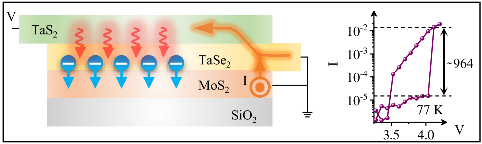
1T-TaS2 exhibits several resistivity phases due to the modulation of charge density wave (CDW). The fact that such phase transition can be driven electrically has attracted a lot of attention in the recent past towards active-metal based electronics. However, the bias-driven resistivity switching is not very large ( 5 fold), and an enhancement in the same will highly impact such phase transition devices. One aspect that is often overlooked is that such phase transition is also accompanied by a significant change in the local temperature due to the low thermal conductivity of 1T-TaS2. In this work, we exploit such electrically driven phase transition induced temperature change to promote carriers over a thermionic barrier in a 1T-TaS2/2H-TaSe2/2H-MoS2 T-Junction, achieving a -fold abrupt switching in the current through the MoS2 channel. The device is highly reconfigurable and exhibits an abrupt reduction in current as well when the biasing configuration changes. The results are promising for several electronic applications, including neuromorphic chips, switching, nonlinear devices, and industrial electronics such as current and temperature sensing.
keywords:
1T-TaS2, charge density waves, phase transitions, current switching, negative differential resistanceMehak Mahajan Kausik Majumdar*
Mehak Mahajan, Dr. Kausik Majumdar
Department of Electrical Communication Engineering
Indian Institute of Science
Bangalore 560012, India
Email Address: kausikm@iisc.ac.in
1 Introduction
The charge density wave (CDW) driven phase transition in layered materials like TaS2, TaSe2, NbSe2, and TiSe2 has attracted a lot of attention in the recent past due to their structural, thermal, magnetic, electrical and optical properties [1, 2, 3, 4, 5]. Out of all these, 1T-TaS2 exhibits polymorphic states with distinctive resistive phases, that can be achieved by thermal [6, 7], mechanical [8, 9], optical [10, 11], and electrical [12, 13] excitation. On heating, 1T-TaS2 transits from commensurate (C) to triclinic (T) phase at K, T to non-commensurate (NC) phase at K, NC to incommensurate (IC) phase at K and IC to metallic phase at K. On the other hand, 2H-TaSe2 that undergoes C to NC phase transition at K and NC to metallic phase at K shows a slight change in slope of resistance versus temperature curve. Unlike 1T-TaS2, 2H-TaSe2 does not exhibit a sharp change in the resistance during the phase transitions.
The fact that in 1T-TaS2, the resistance switching through such phase transitions can be obtained through Joule heating by electrical driving [12, 13, 14], has led to several electronic and optoelectronic device applications [15, 16, 10, 17]. The resistance switching ratio plays an important role in determining the performance of these devices. However, the degree of the resistance switching is often weak, less than [12, 13, 16], depending on the flake thickness, measurement temperature, and crystal quality. Any technique that can enhance the ratio of the resistance switching will be of great importance in such phase transition-based device applications. In this work, we propose a method using a 1T-TaS2/2H-TaSe2/2H-MoS2 T-junction, where we achieve a gate-controllable current switching ratio up to driven by CDW phase change in 1T-TaS2 - which is more than -fold enhancement in the switching ratio compared to existing reports. The principle of operation of the technique exploits the abrupt change in the junction temperature due to an abrupt change in the current resulting from Joule heating induced CDW phase transition in TaS2. This, in turn, helps to promote carriers over a thermionic barrier, modulating the net probe current. Interestingly, the proposed device is electrically reconfigurable between a positive jump (enhancement in current) and a negative jump (reduction in current). Such reduction in current can be modeled as an effective negative differential resistance (NDR), as shown earlier [17].
2 Results and Discussion
The 3D schematic diagram of the proposed triple layered T-junction is shown in Figure 1a. The inset of Figure 1b shows the optical image of the device Da fabricated by exfoliating a few layer MoS2 flake on Si/SiO2 substrate followed by layer-by-layer dry transfer of TaSe2 and TaS2 flakes respectively (see the experimental section for complete fabrication steps). The current (I) - voltage (V) characteristics of the TaS2/TaSe2 junction of the device Da probed between terminals T and TS (with terminal M kept open) at K are shown in Figure 1b. The abrupt hysteretic jump in the current () results from the reduction in the TaS2 resistance owing to electrically driven NC-IC CDW phase transition. Note that TaSe2 being highly conductive, carries ample current to drive NC-IC phase transition of TaS2 in TaS2/TaSe2 junction [3]. Also, the low thermal conductivity of TaSe2 compared to Au contact further aids in raising the local temperature of the channel [18, 19]. The current jump can be further enhanced at low temperatures by invoking phase transition through multiple metastable states of TaS2 using the external electric field [16, 10]. Figure 1c depicts the I-V characteristics of the TaS2/TaSe2 junction of the device Da at K showing a current jump of . Note that when a material with lower conductivity (such as SnSe2) replaces the series resistance material (that is, TaSe2), the overall current is suppressed, which reduces the Joule heating. Hence, the phase transition in TaS2 does not occur anymore (Supplementary Figure S1).
The current-voltage characteristics of TaSe2/MoS2 junction (probed between terminals TS and M keeping terminal T open) and TaS2/MoS2 junction (probed between terminals T and M keeping terminal TS open) as a function of back-gate voltage () varying from V to V in steps of V at K are outlined in Figure 1d and 1e respectively. The forward and reverse sweep directions of the voltage during measurement (indicated by the black arrows in Figure 1d-e) show negligible hysteresis, suggesting excellent interface quality in the device. The corresponding gate-dependent current-voltage characteristics of both the junctions at K are depicted in supplementary Figure S2a and S2b respectively.
2.1 Reconfigurable abrupt current switching in T-junction
We now show the characteristics of 1T-TaS2/2H-TaSe2/2H-MoS2 T-junction that is reconfigurable between abrupt current increment and decrement by utilizing the modulation of the MoS2 resistance through an external gate voltage. In this device, we pass a high current through a voltage bias through the TaS2/TaSe2 path and use the branched out MoS2 channel current as a probe. The equivalent circuit diagram of the four terminal device Da is shown in Figure 2a wherein R1, R2 and R3 correspond to the effective resistance of TaSe2, TaS2 and MoS2 flakes respectively. Here, R3 includes both the TaSe2/MoS2 Schottky junction resistance and the MoS2 channel resistance, and both the components are tunable by the gate voltage. A global back gate is connected to the fourth terminal of the device. Figure 2b shows the variation of MoS2 channel current (IM) with VTS of the device Da when we apply the bias at TS terminal while keeping T and M terminals grounded. The characteristics show current decrement behaviour for both VTS V and VTS V for varying from V to V in steps of V at K. When the external bias exceeds the threshold voltage for the NC-IC phase transition of TaS2, the TaS2 resistance abruptly reduces resulting in the abrupt increment in the TaS2 current, and hence a simultaneous reduction in the MoS2 current. The peak-to-valley current ratio (PVCR) obtained for VTS V and VTS V at K are shown in bottom panel of Figure 2g. A simplistic way to further improve the PVCR values is by increasing the switching ratio of the TaS2 resistance, which directly regulates the abrupt change in the MoS2 current. A base temperature lower than the C-T phase transition temperature can be utilized to achieve such enhancement. We operate the device (Da) at a temperature below the C-T transition temperature to invoke field-driven metastable states of TaS2 that increase the abrupt current jump by in comparison to room temperature. Figure 2c depicts IM versus VTS characteristics delineating current decrement at K. The corresponding PVCR values at K are shown in the top panel of Figure 2g reaching a maximum value of at V for VTS V which is higher in comparison to the room temperature values.
Suppose we apply the bias at the TaS2 terminal while keeping terminals TS and M grounded as depicted in the equivalent circuit in Figure 2d. In that case, the MoS2 current exhibits an abrupt increment instead of a decrement at the phase transition. When we apply a high electric field across the TaS2/TaSe2 junction, the TaS2 phase transition occurs, which reduces the resistance of the TaS2 branch resulting in the abrupt increment in the TaS2 current as well as the MoS2 current. Here, the total current flow through R2 instead of R1 (in the case of TaSe2 biasing) as shown by the arrows in Figure 2d. Figure 2e and 2f shows the gate voltage () dependent current increment characteristics for both VT V and VT V at K and K, respectively. The corresponding current increment factor as the function of for both K and K is shown in Figure 2h. Current increment factor reaches a maximum value of at K for VT V which is higher than the room temperature value.
The low-temperature current increment factor of cannot solely result from phase transition induced resistance switching of TaS2 as it is limited to a factor of as shown in Figure 1c. In addition to 1T-TaS2, 2H-TaSe2 also exhibits CDW phase transitions at K and K. However, it does not cause any abrupt discontinuity in the TaSe2 resistance apart from a slight slope change in resistance versus temperature curve [20, 21, 3]. The overall change in resistance of the TaSe2 branch from the estimated temperature values (discussed later) is small and rules out the contribution of TaSe2 resistance change to the current jump. Also, the heat equation solution of the channel and the in-situ Raman measurement exclude the possibility of structural phase transition of MoS2 from the semiconducting (2H) to metallic (1T) phase. The abrupt current increment due to the TaS2 phase transition increases the local temperature along the device channel. The one-dimensional heat equation solution (using FEM) for the TaS2/TaSe2 channel estimates that the local temperature increment due to Joule heating is sufficient to invoke TaS2 phase transitions (see Supplementary Figure S3), depending upon the base temperature as well as the external bias. However, it is not enough to induce structural 2H to 1T phase transition in MoS2 [22]. This argument is further supported by bias-dependent Raman measurement (see Supplementary Figure S4), wherein j-peaks have not been observed, which could otherwise confirm the presence of the 1T-phase of MoS2.
Such a large current increment can be explained by the enhanced thermionic carrier injection across the TaSe2/MoS2 barrier with a sudden increase in the junction temperature resulting from the Joule heating induced phase transitions of TaS2, as detailed next. The mechanism is schematically illustrated in Figure 3a-b. The abrupt jump in temperature due to the CDW phase transition in TaS2 causes a corresponding increment in temperature at the TaSe2/MoS2 junction due to efficient heat conduction through the TaS2/TaSe2 interface. That, in turn, enhances the kinetic energy of the carriers, helping them overcome the TaSe2/MoS2 Schottky barrier.
2.2 Giant current increment driven by thermionic switching
To explore the thermionic effect due to local temperature switching, we fabricate another triple layered T-junction (Db) comprising a narrow MoS2 channel with a reduced junction overlap area (see the optical image in the inset of Figure 4a). Here we choose a small junction overlap area between MoS2 and the TaS2/TaSe2 to further increase the temperature by forcing the hot electrons to pass through a smaller region. Apart from weaker heat dissipation efficiency, the smaller junction area helps in two other ways. First, when the junction area is small, the fractional contribution of the junction resistance to the total device resistance increases. That helps to achieve a larger switching ratio since the hot carriers, due to the phase transition-induced temperature change, primarily modulate the junction resistance. Second, a smaller overlap area helps to remove any trapped residue and air from the interface during annealing, which in turn helps to achieve closer proximity between MoS2 and TaSe2/TaS2 heater, helping the MoS2 layer to achieve a higher temperature effect at the junction during the switching. IM versus VT of device Db for selective values varying from V to V (step size: V) at K for VT V is depicted in Figure 4a. Similarly, Figure 4b shows the IM versus VT for VT at equal to V, V and V. The corresponding current increment factors during the phase transition are plotted in Figure 4c showing a maximum value of at V for VT V at K which is higher in comparison to the current increment factor of device Da.
At low temperature, we could further enhance the current jump as depicted in IM versus VT characteristics of device Db at K (see Figure 4d and 4e for VT V and VT V, respectively) for different values. The corresponding current increment factors are plotted in Figure 4f for both VT V and VT V. We could enhance the MoS2 current by a factor of at V for VT V as represented in Figure 4f. As discussed earlier, such a huge jump can not solely arise from electrically driven TaS2 phase transition. And, we must invoke the corresponding sudden rise in the junction temperature due to the abrupt enhancement in current through TaS2/TaSe2 during the CDW phase transition of TaS2. Figure 4g depicts the variation of the current increment factor as a function of at a base temperature of K, K, and K for VT V. Such a strong temperature dependence in the current increment factor suggests possible usage of the technique in sensing temperature.
In Figure 4f for , the current jump ratio at the phase transition exhibits a strong non-monotonic behavior with . Also, the ratio shows an opposite trend for , particularly when . The origin of such behavior is explained in Figure 5. In the case of VT V, that is, when MoS2 injects electrons into TaSe2, there are three different regions of device operation (viz. A, B, and C as shown in Figure 4c and 4f) as schematically explained in Figure 5a. Note that, due to the high electrical conductivity of TaSe2 in comparison to TaS2 (in particular, at a low temperature), the floating voltage at the triple junction is small; hence the drop across the MoS2 channel is also small (estimated to be mV). Due to such a small effective drain voltage, the current through the MoS2 channel strongly depends on the drain barrier as well in the different regimes of operation. In the current situation, where TaSe2 acts as the drain contact for configuration, the drain barrier plays an even more important role. We recently found that due to van der Waals nature of the contact interface, TaSe2 exhibits strong Fermi level depinning [23] with layered semiconductors. Accordingly, due to the relatively large work function of TaSe2, the conduction band offset between MoS2 and TaSe2 is large. On the other hand, due to Fermi level pinning, Ni/MoS2 junction has a relatively small Schottky barrier height [24]. That leads to a larger drain barrier compared to the source barrier at the small effective drain bias as schematically shown in Figure 5a, and hence the TaSe2/MoS2 interface controls the drain current.
In region A, that is, for V, electrons do not see any barrier at the drain side and can quickly transfer into TaSe2 (see top panel of Figure 5a). Thus, the current does not change much with the abrupt increase in temperature during the CDW phase transition. In region B, the electrons from the MoS2 region require to overcome the drain barrier to be transferred to TaSe2 (see middle panel of Figure 5a), and thus the current is a strong function of the local temperature at the drain barrier. The current induced Joule heating can increase the local temperature to K for a base temperature of K (see Supplementary Figure S3 for simulated results). The current jump ratio simulated for various barrier heights ( varying from to meV) by solving modified Richardson’s equation [24] at temperatures of K, K, K, K and K with respect to K is shown in Supplementary Figure S5. The simulation results clearly show that the current ratio before and after the phase transition can go as high as depending upon . That justifies the high current increment factor at V. Finally, in region C for V, the band bending increases, and the electrons can tunnel through the Schottky drain barrier, as shown in the bottom panel of Figure 5a. Thus, the local temperature does not affect the current, reducing the current ratio before and after the phase transition. Beyond region C, at an even higher positive , we observe an increment in the current increment factor, the origin of which is yet not very clear and could result from a dependent change in the relative resistance between the source and the drain barriers.
On the other hand, for VT V, TaSe2 acts as a source contact, and the electrons are injected from TaSe2 to the MoS2 channel. At high negative , i.e., region D, the carrier injection is determined by thermionic transport over the Schottky barrier height at TaSe2/MoS2 interface, as shown in the top panel of Figure 5b, and hence contributes to higher current jump. However, for V (region E), the current increment ratio decreases monotonically as the carrier injection is dominated by the tunneling phenomenon schematically shown in the bottom panel of Figure 5b.
In similarity to device Da, the IM versus VTS characteristics of device Db exhibits current decrement for VTS biasing at both K and K (see Supplementary Figure S6). The corresponding IM versus VT (depicting current increment) and IM versus VTS (depicting current decrement) characteristics for device Db at K and K are outlined in Supplementary Figure S7 and S8 respectively. The current increment characteristics have been repeatedly observed in several devices, some of which are outlined in Supplementary Figure S9 and S10.
3 Conclusion
The technique proposed in this work demonstrates a unique way of significantly amplifying the resistance switching ratio typically obtained from a TaS2 CDW phase transition. That is achieved by exploiting enhanced carrier injection through a Schottky barrier height by the abrupt increment in the local temperature during the phase transition. Accordingly, the technique can be applied to enhance the device performance in several applications where TaS2 phase transition is used, for example, in detecting infrared photons and neuromorphic applications. In addition, the gate tunable sharp jump in current can be useful for sensing applications, such as temperature and current. On the other hand, the enhancement in the MoS2 channel current during the CDW phase transition of TaS2 provides an excellent probe to monitor the local temperature of TaS2.
4 Experimental Section
Triple Layered T-Junction Device Fabrication and characterization. 1T-TaS2/2H-TaSe2/2H-MoS2 T-junction is fabricated in the following manner. First, the thin flakes of MoS2 are mechanically exfoliated on a heavily doped Si substrate coated with nm thick SiO2 using polydimethylsiloxane (PDMS), followed by dry transfer of TaSe2 and TaS2 flakes respectively. A rotational stage controls the alignment during each layer transfer to form the T-junction. The complete exfoliation and dry transfer processes are done at room temperature. The substrate is then spin-coated with a high contrast positive resist polymethyl methacrylate (PMMA) C and softly baked for minutes at ∘C. Patterns are formed through electron beam lithography with an electron beam dose of C cm-2, an electron beam current of pA, and an acceleration voltage of KV. The pattern development is carried out in MIBK/IPA developer solution followed by IPA wash and blow drying in N2. Metal contacts are formed by blanket deposition of nm Ni / nm Au using a DC magnetron sputter coating system in the presence of Ar plasma at Torr. Excess metal lift-off is carried out by immersing the substrate in acetone for minutes, followed by IPA wash for seconds and blow drying in N2. Buffered HF solution is used to etch the back oxide from the substrate, and highly conducting silver paste is used for the back gate contact.
The electrical measurements are carried out in a probe station with a base vacuum level of about Torr at room temperature and Torr at the low temperature with the supply of liquid N2.
Supporting Information
Supporting Information is available from the Wiley Online Library or from the author.
Acknowledgements
This work was supported in part by a Core Research Grant from the Science and Engineering Research Board (SERB) under Department of Science and Technology (DST), a grant from Indian Space Research Organization (ISRO), a grant from MHRD under STARS, and a grant from MHRD, MeitY and DST Nano Mission through NNetRA.
References
- [1] M. S. El-Bana, D. Wolverson, S. Russo, G. Balakrishnan, D. M. Paul, S. J. Bending, Superconductor Science and Technology 2013, 26, 12 125020.
- [2] B. Yan, B. Zhang, H. Nie, G. Li, X. Sun, Y. Wang, J. Liu, B. Shi, S. Liu, J. He, Nanoscale 2018, 10 20171.
- [3] M. Mahajan, S. Kallatt, M. Dandu, N. Sharma, S. Gupta, K. Majumdar, Communications Physics 2019, 2, 1 88.
- [4] E. Zhang, X. Xu, Y.-C. Zou, L. Ai, X. Dong, C. Huang, P. Leng, S. Liu, Y. Zhang, Z. Jia, X. Peng, M. Zhao, Y. Yang, Z. Li, H. Guo, S. J. Haigh, N. Nagaosa, J. Shen, F. Xiu, Nature Communications 2020, 11, 1 5634.
- [5] W. Li, G. V. Naik, Applied Physics Letters 2021, 118, 25 253104.
- [6] R. Manzke, T. Buslaps, B. Pfalzgraf, M. Skibowski, O. Anderson, Europhysics Letters (EPL) 1989, 8, 2 195.
- [7] A. H. Thompson, R. Gamble, J. Revelli, Solid State Communications 1971, 9 981.
- [8] K. Bu, W. Zhang, Y. Fei, Z. Wu, Y. Zheng, J. Gao, X. Luo, Y.-P. Sun, Y. Yin, Communications Physics 2019, 2, 1 146.
- [9] S. S, H. K. Kundu, P. Vishnubhotla, A. Bid, Phys. Rev. Materials 2021, 5 124003.
- [10] C. Zhu, Y. Chen, F. Liu, S. Zheng, X. Li, A. Chaturvedi, J. Zhou, Q. Fu, Y. He, Q. Zeng, H. J. Fan, H. Zhang, W.-J. Liu, T. Yu, Z. Liu, ACS Nano 2018, 12, 11 11203.
- [11] W. Li, G. V. Naik, Nano Letters 2020, 20, 11 7868, pMID: 32816498.
- [12] M. J. Hollander, Y. Liu, W.-J. Lu, L.-J. Li, Y.-P. Sun, J. A. Robinson, S. Datta, Nano Letters 2015, 15, 3 1861.
- [13] M. Yoshida, T. Gokuden, R. Suzuki, M. Nakano, Y. Iwasa, Phys. Rev. B 2017, 95 121405.
- [14] M. Mahajan, K. Murali, N. Kawatra, K. Majumdar, Phys. Rev. Applied 2019, 11 024031.
- [15] M. Yoshida, R. Suzuki, Y. Zhang, M. Nakano, Y. Iwasa, Sci Adv 2015, 1, 9 e1500606.
- [16] G. Liu, B. Debnath, T. R. Pope, T. T. Salguero, R. K. Lake, A. A. Balandin, Nature Nanotechnology 2016, 11, 10 845.
- [17] M. Mahajan, K. Majumdar, ACS Nano 2020, 14, 6 6803, pMID: 32406676.
- [18] M. D. Núñez Regueiro, J. M. Lopez-Castillo, C. Ayache, Phys. Rev. Lett. 1985, 55 1931.
- [19] B. Huettner, Femtosecond Laser Pulse Interactions with Metals, 315–337, ISBN 978-1-4020-9339-5, 2009.
- [20] H. N. S. Lee, M. Garcia, H. L. McKinzie, A. Wold, Journal of Solid State Chemistry 1970, 1 190.
- [21] M. Naito, S. Tanaka, Journal of the Physical Society of Japan 1982, 51, 1 219.
- [22] D. Y. Hwang, K. Choi, D. Suh, Nanoscale 2018, 10.
- [23] K. Murali, M. Dandu, K. Watanabe, T. Taniguchi, K. Majumdar, 2021 .
- [24] D. Somvanshi, S. Kallatt, C. Venkatesh, S. Nair, G. Gupta, J. K. Anthony, D. Karmakar, K. Majumdar, Phys. Rev. B 2017, 96 205423.
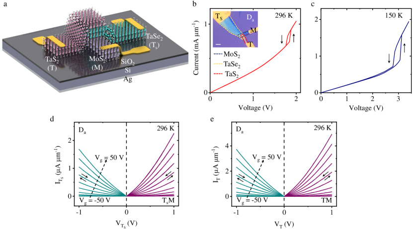
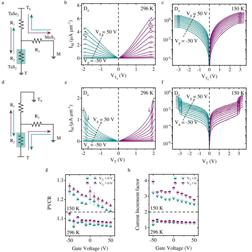
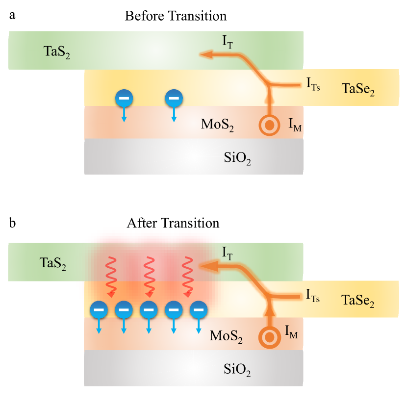
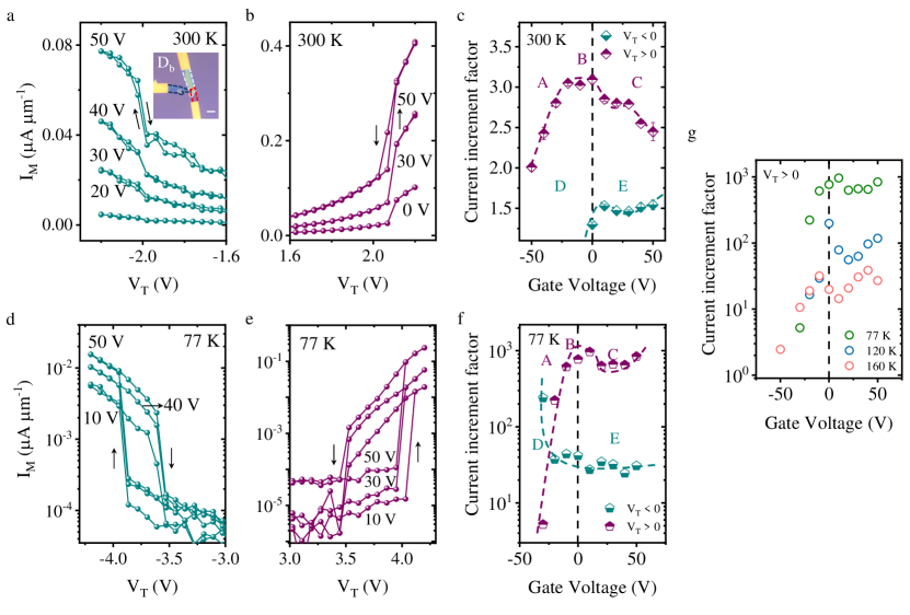
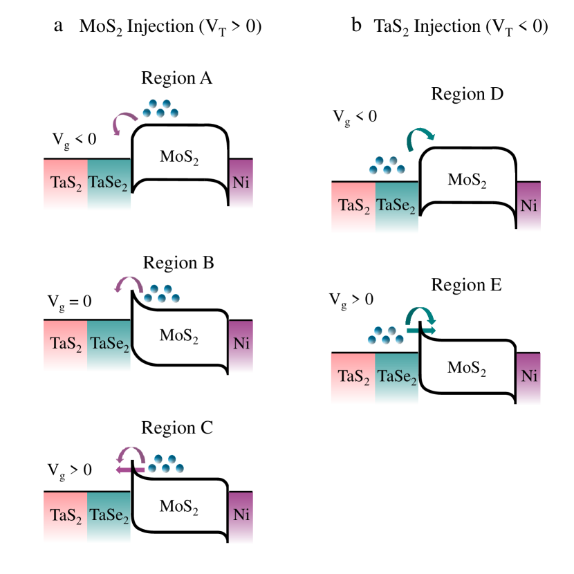
Table of Contents