Demystifying the Nvidia Ampere Architecture through Microbenchmarking and Instruction-level Analysis
Abstract
Graphics processing units (GPUs) are now considered the leading hardware to accelerate general-purpose workloads such as AI, data analytics, and HPC. Over the last decade, researchers have focused on demystifying and evaluating the microarchitecture features of various GPU architectures beyond what vendors reveal. This line of work is necessary to understand the hardware better and build more efficient workloads and applications. Many works have studied the recent Nvidia architectures, such as Volta and Turing, comparing them to their successor, Ampere. However, some microarchitecture features, such as the clock cycles for the different instructions, have not been extensively studied for the Ampere architecture. In this paper, we study the clock cycles per instructions with various data types found in the instruction-set architecture (ISA) of Nvidia GPUs. Using microbenchmarks, we measure the clock cycles for PTX ISA instructions and their SASS ISA instructions counterpart. we further calculate the clock cycle needed to access each memory unit. We also demystify the new version of the tensor core unit found in the Ampere architecture by using the WMMA API and measuring its clock cycles per instruction and throughput for the different data types and input shapes. The results found in this work should guide software developers and hardware architects. Furthermore, the clock cycles per instructions are widely used by performance modeling simulators and tools to model and predict the performance of the hardware.
Index Terms:
Instructions Latency, Tensor core throughput, PTX, SASS, Ampere.I Introduction
Graphics processing units (GPUs) have significantly increased in accelerating general-purpose applications from neural networks to scientific computing. GPUs are now considered the main hardware component in any high-performance supercomputer. For instance, Meta built one of the fastest supercomputers based on Nvidia Ampere architecture GPUs (A100) [1], and they are extending it to be the most powerful supercomputer in the world by mid-2022. Besides, tens of the top500 supercomputers [2] are GPU-accelerated.
Nvidia provides a new architecture generation with updated features every two years with little micro-architecture information about these features, making it difficult to quantify. This raises the need to study the effect of new features on the performance of applications. Nvidia introduced the tensor core (TC) unit to accelerate deep neural networks with the introduction of Volta. This version of TC operates on FP16 and FP32 precision operations. Ampere architectures added a sparsity feature and new data precisions for the TC such as Int8, Int4, FP64, bf16, and TF32. Usually, there is little information beyond what the vendors choose to reveal in their whitepapers, which raises the need to quantify these features. Thus, researchers try to explain and demystify the new features of each GPU generation [3, 4, 5, 6, 7, 8]. However, some areas still have not been fully covered in the literature. In this work, we focus on demystifying the clock cycle latency at the granularity of the instructions in the Instruction-set architecture (ISA). Similar work has been proposed before. For instance, the authors in [9] adapted some microbenchmarks to demystify some hardware units such as the memory, the tensor cores, and the arithmetic units. However, they only calculated the latency for memories at the granularity of the warp and the block, not the instructions. In another work [10], the authors calculated the latencies for only the memory hierarchy of older generations.
This paper presents microbenchmark analyses to dissect the instruction clock cycles per instructions for the Nvidia Ampere GPU architecture [11]. The microbenchmarks presented in this work are based on Parallel Thread Execution (PTX) [12]. PTX is an intermediate representation between the high-level language (CUDA) and the assembly language (SASS). So, it is portable among different architectures. PTX is open-source and well documented. However, its instructions do not directly execute on the hardware. It has to be converted to another architecture-dependent ISA. SASS, in this case, is closed-source and compatible only within each architecture family. This paper shows how each PTX instruction is mapped to SASS instruction while measuring the clock cycles for both ISAs. Furthermore, we present the clock cycle needed to access each memory unit. The microbenchmarks are based on a previous work by Arafa et al. [13], which calculated the clock cycle latencies for various instructions on different Nvidia architectures. However, there are no such studies done on the Ampere architecture. We also show the clock cycles and throughput for tensor core instructions on different data types.
Measuring the instructions clock cycles helps predict performance by GPU modeling tools. For instance, Arafa et al. [18] showed that by adopting correct latency for the GPU instructions, their performance model can improve its prediction accuracy compared to the actual hardware. Furthermore, Andersch et al. [10] have proven the critical relationship between the latencies and the performance. This work is the first step in accurately modeling the Ampere GPU architecture.
The main contributions of this paper are as follows:
-
•
We demystify the Nvidia Ampere [11] GPU architecture through microbenchmarking by measuring the clock cycles latency per instruction on different data types.
-
•
We show the mapping of PTX instructions to the sass instructions while measuring the clock cycles for both.
-
•
We calculate the Ampere architecture tensor cores instructions (WMMA) clock cycle latency and throughput while clarifying their PTX and SASS instructions.
-
•
We measure the access latency of the different memory units inside the Ampere architecture.
II Background
Unlike multi-core CPUs, which have several powerful processors, GPUs have tens of simple processors that can work simultaneously to perform a specific task efficiently. This is viable for many applications that require numerous work to be performed in parallel, such as artificial intelligence and scientific computing.
An Nvidia GPU consists of several streaming multiprocessors (SM). The number of SMs varies with the generation of the GPU. Older architectures, such as Kepler, have fewer SMs (15 or 24), while contemporary architectures, such as Ampere, have a more significant number (124). The computation resources inside the SMs also vary depending on the architecture generation. Each SM is divided into hundreds of small cores performing different operations. GPUs have different types of memory units. The global memory and L2 cache are shared with all SMs. Furthermore, it has L1 caches, which are private to each SM. Moreover, threads inside a block can communicate through the shared memory.
The need for GPUs in many essential fields nowadays forces the vendors to enhance their GPU architecture to provide better performance. NVIDIA provides a new architecture every two years. New architectures not only have new hardware units but also may contain new ISA that increases performance. For example, in the Ampere architecture, Nvidia introduced much enhancement in the tensor core unit, making it faster and run on larger matrices. Moreover, it introduced the new L2 cache residency control feature, which automatically manages data to keep or evict from the cache.
Although these features are well documented in the whitepaper and online review websites, there are little information on the microarchitecture and the instruction-level enhancements found in the recent Ampere architecture. This paper fills this gap by providing a detailed instruction-level characterization of the Ampere GPU’s instruction-set architecture (ISA).
III Related work
Various work have been conducted to dissect every undisclosed microarchitecture characteristic of the GPU [13, 19, 20, 7, 8, 21] using microbenchmarks. Unlike the Nvidia Ampere architecture, the older architectures such as Kepler, Fermi, Volta, and Turing are heavily studied in the literature. Some focused on the instruction level [6, 13], while others focused on the hardware unit itself [20, 22, 23]. In this section, we present some of these works in more detail.
Wong et al. [6] was the first to introduce microbenchmarks to measure the latency and the throughput of different types of memories and instructions. In [9], the authors modified some microbenchmarks to isolate the GPU features and study each separately. They studied the effect of the number of warps and blocks on the throughput for the memory, arithmetic, and tensor cores operations. They calculated the latencies per block, not per instruction. Other works [24, 7, 8] calculated instructions and memory throughput and latencies for the Kepler, Volta, and Turing architectures. However, [24] added more details about energy consumption. In the same spirit, Mei et al. [20] presented a microbenchmark for calculating the throughput and latencies of different types of memory units on older architectures such as Fermi, Kepler, and Maxwell.
Other researchers focused on profiling the tensor core in Volta and Turing architectures [22, 25, 26]. Recently, Sun et al. [21] tried to dissect the tensor core in the Ampere architecture. The authors focused on investigating the matrix multiply-accumulate using the MMA API, which gets executed on the tensor cores. They did not provide results for the WMMA API. In [27], the authors demonstrated the mapping of the PTX to the SASS instructions for the tensor core operations. Fasi et al. [23] developed a microbenchmark to investigate the tensor core numerical behavior and proved that the tensor core supports the subnormal number.
While all the previous work presents good progress, none focused on the clock cycles latency for all data types of each instruction while demonstrating the PTX and SASS mapping for each instruction. Moreover, to the best of our knowledge, we are the first to investigate every WMMA Tensor Core instruction clock cycles and throughput with different data types for the Nvidia Ampere architecture. Finally, Our work can be easily extended for future architectures.
IV Methodology
In this section, we introduce the microbenchmark design details. Our work is based on extending the microbenchmark presented in [13] to calculate the clock cycles per instruction for the Nvidia Ampere (AI100) GPU. We modified the microbenchmark to calculate the latency for dependent and independent instructions. Furthermore, we extended the code to calculate the clock cycles latency for the different types of memory units and the tensor core instruction.
The microbenchmarks are directly written in PTX, a pseudo assembly intermediate and architecture-independent ISA across all Nvidia. However, writing directly in PTX ISA can be tricky since the compiler translates the PTX code into another architecture-dependent ISA, SASS. There is not much information available on how the compiler does the mapping from PTX to SASS. For instance, the compiler can optimize multiple PTX instructions into one SASS instruction. In order to overcome these limitations and ensure the proper instructions get executed are the ones we need, we dynamically read the SASS instruction trace at the run time of each PTX microbenchmark written. We use the Tracing Tool from PPT-GPU [17] to do that. We then tweak the PTX microbenchmark by trial and error to give us the correct SASS results.
IV-A Instructions Clock Cycles Latency
We used only one thread per block to measure the instruction latency. We have two steps. First, We run a code that calculates the clock cycles for the studied instruction with a specified data type. For instance, the code shown in Figure 2 calculates the latency of the add instruction where the operands are 32-bit registers. In general, measuring the latency can be performed by reading the clock before and after the instruction, as shown in Figure 2 lines 13 and 17. Then, we subtract the two clock readings (line 18) to calculate the difference or the required latency. We execute the three independent add instructions (lines 14-16). We also used dependent instructions and found that latency increased compared to independent instructions. Finally, we return the latency value to the main CUDA function and divide it by 3 to calculate the number of cycles for each instruction. We use 3 instructions to overcome the first launch overhead. We found that executing only one instruction will result in an unexpected higher number of cycles. Table I shows an example for add.u32 instruction. The first instruction takes around 5 cycles. Nevertheless, when we use more than 3 instructions, the average number of cycles per instruction (CPI) is 2.
| # instrs | CPI |
| 1 | 5 |
| 2 | 3 |
| 3 | 2 |
| 4 | 2 |
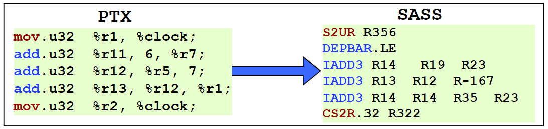
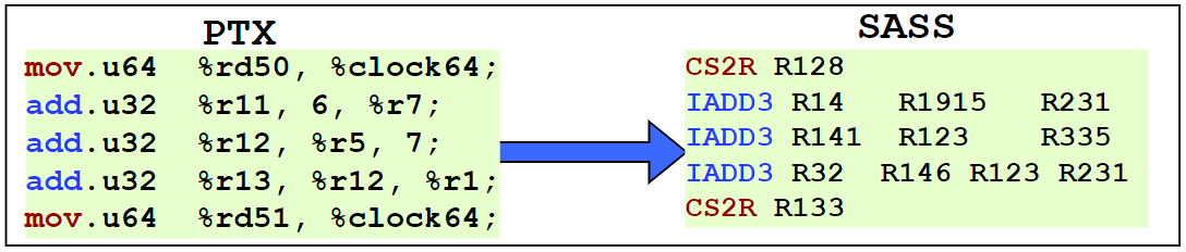
Second, we inspect the sass instruction using the dynamic Tracing Tool from PPT-GPU [18] to ensure that the mapping from PTX to SASS is correct and no additional overhead or instruction is added at runtime by the compiler. The PTX code shown in Figure 4(a) provides an inaccurate latency for the add instruction when storing the clock in 32-bit registers. The dynamic SASS instruction trace shows a barrier between the two clock readings, as shown in the second instruction of the SASS part. This barrier causes a considerable change in the results (around 33 cycles increase in this case). One method to overcome this barrier is to use the 64-bit registers to store the clocks, which remove the barrier and provide an accurate measurement, as shown in Figure 4(b). The CPI for the first and second cases are 13 and 2 cycles, respectively. Finally, we calculate the clock overhead using two consecutive clock reading instructions and find that it equals 2 cycles.
IV-B Memory Units Access Latency
To calculate global, L2, and L1 cache memories latency, we use a pointer chasing technique, in which each array elements are dependent on the previous ones. This technique forces the reading operations to be serialized to calculate the latency correctly. Otherwise, many reading operations can be issued simultaneously, which makes the latency measurements inaccurate. Figure 2 shows the PTX microbenchmark for the memory latency calculations. Line 1 moves the array address to the %r19 register. Then, we start a counter with a zero value in the %r40 register. This counter is used to iterate over the array of elements. Lines 3 and 9-11 represent the loop instructions. Lines 4 to 7 are used to store the array of elements in which each element is dependent on the previous one. After storing the results, we use the instructions from lines 14 to 24 to read the clocks while reading every element in the array. From 16 to 19, we have 4 load instructions to load 4 values, which are repeated to read all the array elements.
The ld instruction can be used with many operators such as cv, ca, and cg. Each operator has its usage. ca is used to cache on all available levels (global-L1-L2) while the cg caches only in L2. On the contrary, we use cv because it bypasses the caches, which we need when we calculate the global memory latency. We use 4 instructions because we found that in many cases, the compiler unrolls the loops by 4 when we inspected the dynamic trace of some Cuda applications that use loops. The difference between the global memory code and the l2 cache code is the operator used with the ld instruction and the number of the elements in the array. For the L2 cache, we use the cg operator, and the total size of the array elements must be less than the L2 size, while for the global memory code, it must be larger than the L2 cache to avoid L2 cache residency. Likewise, we repeat the same methodology with the ca operator to calculate the L1 cache latency.
For the shared memory, we load and store instructions between reading the clocks, as shown in lines 3-12 of Figure 3. However, we needed to add another instruction that depends on the ld or st instructions to prevent the compiler from executing the clock reading instruction before finishing, as shown in lines 4-13.
IV-C Tensor core Instructions Latency and Throughput
The Tensor core (TC) unit is a very trivial unit for accelerating machine learning applications. Each SM in the Ampere architecture contains 4 tensor cores that can run the multiple-add operation on 3 matrices in the form D=A*B+C where A, B are the inputs and C, D are the accumulators. Unlike the Volta, which supports only fp16 precision for the inputs, the Ampere architecture supports many types, such as FP16, bf16, tf32, f64, u8, u4 and the single bit. The general arithmetic instructions use one thread to execute and can communicate only through the global or shared memory. On the other hand, the TC instructions use all the 32 instructions in the dedicated warp. To demystify the Ampere architecture’s TC instructions with the new data types, we designed a special microbenchmark is written in Cuda programming language. The microbenchmarks are inspired by Jia et al. [7] work, which focused on Volta architecture.
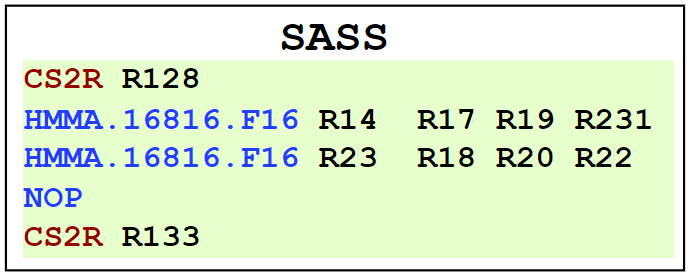
Some of the new data types that were introduced in the Ampere architecture are still in the experimental stage, as mentioned in PTX and CUDA documentation [28]. Moreover, because each data type has its shapes, stride, and layout, we use a different function to calculate the latencies of each type. Figure 5 shows the code used to calculate the TC instruction latency of U8 data type. Lines 5 to 7 create a fragment in which the registers are prepared to get the matrix elements to be stored. We create 4 fragments; however, we do not write all to make the shape smaller. Then, we load the data from memory (lines 10-12), and the same goes for the other fragments. As previously explained, we read the clocks before and after the TC WMMA execution (lines 15 to 22) and subtract them before printing, as shown in lines 28-29. From lines 16 to 21, we run 4 TC instructions (1 per TC) numerous times. We used 4 instructions because we found that calculating the latency from one TC with one instruction provides inaccurate measurement. For example, Figure 6 shows the dynamic SASS instructions of running one instruction on one TC. The NOP instructions refer to a warp synchronization in PTX, and we found that the latency here is not the same as mentioned in the white paper. This also happens when we run one instruction several times. Finally, we calculate the latency per instruction and print them by lines 28-29. A similar method is used to calculate the TC’s WMMA throughput.
V Results
In this section, we present the detailed setup and results. We first show the instructions clock cycles latency. Next, we explain the memory access latencies. Finally, We present the Tensor Core latency and throughput. We run all the microbenchmarks on the Nvidia Tesla AI100 GPU.
V-A Instructions Latency
We found that dependency directly affects the instructions clock cycle latency. Hence, we rerun the microbenchmark with a sequence of dependent instructions (shown in Figure 2), replacing the dependent sequence with another sequence of independent instructions. Table II shows the CPI for dependent and independent sequences for some of the instructions. For instance, single precision add instruction shows 4 and 2 cycles, respectively. We also found that with no dependency, the 3 add.u32 instructions mentioned in Figure 2 are mapped to the same sass instruction (IADD) as shown in Figure 4(a). Nevertheless, PTX instructions may be converted to different instructions when we use three dependent instructions. For example, the add.u32 PTX instruction can be mapped to IADD3 or IMAD.IADD with the dependency case.
Table V depicts the various PTX-SASS instructions with their measured clock cycles latencies. We have a separate PTX kernel (microbenchmark) for each field in the table.
Next, we discuss some additional insights we found while generating the results:
1: The mad instruction runs on the floating pipeline, not the integer pipeline, even if we use it with integer values. This can be proven by the following:
-
•
The PTX instructionmad.lo.u32 in Table V is mapped to the SASS FFMA (floating multiple-add).
-
•
We created a special code that runs two add instructions and two mad instructions using one thread, and we found that the total number of cycles is around 4 cycles. This means that each one of the four instructions takes 1 cycle. It proves that each of the two types is executed simultaneously on different pipelines.
Showing that mad instruction uses another pipeline explains why the dependent PTX add.u23 instruction is mapped to the SASS (IMAD.IADD) instruction in some cases. The compiler is trying to use the floating pipeline while waiting for the integer pipeline to commit.
2: Except for bfind, min and max instructions there is no difference in clock cycles or mapping between PTX to SASS when using a signed or an unsigned instruction. For instance, add.u64 and add.s64 provide the same mapping and the same latency.
3: Usually, a mov or add instruction is used to initialize a register with a value before using this register as an input operand to the instruction that we need to calculate its latency. However, in some cases, we found that the clock cycles and the PTX-SASS mapping change depending on how the inputs are initialized. For example, the PTX neg.f32 is mapped to the SASS FADD when we use add instruction to initialize the inputs. on the other hand, it merges the mov and the neg instructions together in one SASS instruction (IMAD.MOV.u32) when we use mov for initializing. The same happens for the abs.f32 instruction.
| # instrs | CPI for dependent | CPI for independent |
|---|---|---|
| add.f16 | 3 | 2 |
| add.u32 | 4 | 2 |
| add.f64 | 5 | 4 |
| mul.lo.u32 | 3 | 2 |
| mad.rn.f32 | 4 | 2 |
Supported shapes Inputs Accumulators Cycles Measured-theoretical Instructions m16n16k16 - m8n32k16 - m32n8k16 .f16 .f16 16 311-312 GB/s PTX: wmma.mma.sync.aligned.row.row.m16n16k16.f16.f16 SASS: 2*HMMA.16816.F16 – each inst. is 8 cycles m16n16k16 - m8n32k16 - m32n8k16 .f16 .f32 16 310-312 GB/s PTX: wmma.mma.sync.aligned.row.row.m16n16k16.f16.f32 SASS: 2*HMMA.16816.F32 – each inst. is 8 cycles m16n16k16 - m8n32k16 - m32n8k16 .bf16 .f32 16 310-312 GB/s PTX: wmma.mma.sync.aligned.row.row.m16n16k16.f32.bf16.bf16.f32 SASS: 2*HMMA.16816.F32.BF16 – each inst. is 8 cycles m16n16k8 .tf32 .f32 16 132-156 GB/s PTX: wmma.mma.sync.aligned.row.row.m16n16k8.f32.tf32.tf32.f32 SASS: 4*HMMA.1684.F32.TF32 – each inst. is 4 cycles m8n8k4 .f64 .f64 16 19-19.5 GB/s PTX: wmma.mma.sync.aligned.row.row.m8n8k4.f64.f64.f64.f64.rn SASS: 1*DMMA.884 – each inst. is 16 cycles m16n16k16 - m32n8k16 - m8n32k16 .u8 .u32 8 594-624 GB/s PTX: wmma.mma.sync.aligned.row.row.m16n16k16.s32.u8.u8.s32 SASS: 2*IMMA.16816.U8.U8 – each inst. is 4 cycles m8n8k32 .u4 .u32 4 1229-1248 GB/s PTX: wmma.mma.sync.aligned.row.col.m8n8k32.s32.u4.u4.s32 SASS: 1*IMMA.8832.U4.U4 each inst. is 4 cycles
4: Although many PTX instructions have a 1-to-1 mapping to SASS, others such as div, rem, sinf, and cosf are translated to multiple different SASS instructions.
5: Not all instructions with the same data type have the same latency. More specifically, mad.lo.u64 is mapped to an IMAD SASS instruction which takes only 2 cycles. However, the double precision add, sub and fma instructions take 4 cycles each.
6: For the testp instruction, the latency depends on the state.
V-B Memory Access Latencies
The observed latencies of the different types of memories are shown in Table IV. The global memory latency is around 290 cycles. This value does not include the cache misses latencies because we prevent caching at all levels. This number is improved compared to Turing architecture which is 434 cycles [13]. The L2 access latency is 200 cycles compared to 188 cycles for Turing architecture. Furthermore, the L1 cache hit for both Ampere and Truing architectures is 33 and 32 cycles, respectively. For the shared memory, we found that the store access latency takes a smaller value than the load instruction, 23 and 19 for load and store, respectively.
V-C Tensor Core Latencies and Throughput
The Ampere architecture ISA provides various SASS instructions that run on the Tensor Core, which supports the newly added data types. The Volta Architecture’s ISA has only the HMMA.884 SASS instruction handles all Tensor Core operations (single and mixed-precision operations). For Turing, two kinds of the HMMA SASS instructions exist which runs on different input shapes, HMMA.1688 and HMMA.884 [26].
Table III depicts the Ampere architecture’s TC instructions. More specifically, DMMA.884, IMMA.16816 and IMMA.8832 were added to handle the FP64, U8 and U4 data types, respectively. Each PTX instruction of each data type is translated to a different number of SASS instructions. For the FP16 BF16 and U8 inputs, the PTX is translated to 2 instructions. The TensorFloat-32 (TF32) precision is mapped to 4 SASS instructions, while the FP64 and U4 are mapped to only 1 instruction. These differences are related to the difference between the supported PTX shapes and the shapes that the SASS can work on it. For example, in Table III’s first row, the PTX instruction can use many shapes such as 16×16×16, but the SASS can only work on 16×8×16. So, 2 SASS instructions are needed to iterate over the PTX shape. However, the physical TC implementation can perform 8*4*8 [21]. While it is previously mentioned in [25] that the TC latencies are shape-dependent for Turing, we found that different shapes for the same data type do not affect the calculated latency. It can vary from one type to another in Ampere architecture. Our observations for the TC throughput and latencies shown in the table are consistent with the behavior mentioned in the white paper [11]. Finally, We noticed that for all half floating precision (fp16 and bf16) inputs, SASS instruction MOVM.16.MT88 is used for loading a matrix to the TC. In general, the MOVM SASS instruction is used to move a matrix with a transpose. The number of issued MOVM instructions depends on the matrix shape and the layout (row or column major). For example, if we used A and B matrices as row major in the PTX code, then the MOVM instructions are used to transpose the B matrix to multiply each row from A with each column from B. However, when we use both as Column major, the MOVM instruction is used with the A and C matrices. It transposes A and C before execution and transposes C after the execution. Finally, if A is a row-major and B is a column-major, the MOVM instruction does not exist in the trace. We used the same way motioned above for the latency calculations to calculate the memories throughput. The observations are quite similar to the throughput values mentioned in the white paper.
| Memory type | CPI (cycles) |
|---|---|
| Global memory | 290 |
| L2 cache | 200 |
| L1 cache | 33 |
| Shared Memory (ld/st) | (23/19) |
VI Conclusion
This paper demystifies the instructions, memories, and tensor cores for Nvidia Ampere architecture. We perform a detailed analysis of the PTX instructions latency while showing their SASS translation. The presented microbenchmarks are portable and can be extended for future architectures. In addition, we pointed out the microarchitecture instructions of the tensor cores and their latencies for all data types supported by the Ampere architecture. Finally, we calculate the memory latency while building the pointer chasing method for both global memory and L2 cache. This work can help in understating the hardware from the microarchitecture point of view, leading to better-optimized applications and workloads.
PTX SASS cycles PTX SASS cycles Add / sub instruction Min/Max instructions add.u16 UIADD3 2 Min.u16 ULOP3.LUT+UISETP.LT.U32.AND+USEL 8 addc.u32 IADD3.X 2 min.u32 IMNMX.U32 2 add.u32 IADD 2 min.u64 UISETP.LT.U32.AND+2*USEL 8 add.u64 UIADD3.x+ UIADD3 4 min.s16 PRMT+IMNMX 4 add.s64 UIADD3.x+UIADD3 4 min.s32 IMNMX 2 add.f16 HADD 2 Min.s64 UISETP.LT.U32.AND+UISETP.LT.AND.EX+2*USEL 8 add.f32 FADD 2 min.f16 HMNMX2+PRMT 4 add.f64 DADD 4 min.f32 FMNMX 2 Mul instruction min.f364 DSETP.MIN.AND+IMAD.MOV.U32+UMOV+FSEL 10 mul.wide.u16 LOP3.LUT+IMAD 4 Neg instruction mul.wide.u32 IMAD 4 neg.s16 UIADD3+UPRMT 5 mul.lo.u16 LOP3.LUT+IMAD 4 neg.s32 IADD3 2 mul.lo.u32 IMAD 2 neg.s64 IMAD.MOV.U32+HFMA2.MMA+MOV+UIADD3 10 mul.lo.u64 IMAD 2 neg.f32 FADD or IMAD.MOV.U32 * 2 mul24.lo.u32 PRMT + IMAD 3 neg.f64 DADD+(UMOV) 4 mul24.hi.u32 UPRMT+USHF.R.U32.HI+IMAD.U32+PRMT 9 FMA instruction mul.rn.f16 HMUL2 2 fma.rn.f16 HFMA2 2 mul.rn.f32 FMUL 2 fma.rn.f32 FFMA 2 mul.rn.f64 DMUL 4 fma.rn.f64 DFMA 4 MAD Instruction Sqrt Instruction mad.lo.u16 LOP3.LUT+IMAD 4 sqrt.rn.f32 [multiple instrs including MUFU.RSQ] 190-235 mad.lo.u32 FFMA 2 sqrt.approx.f32 [multiple instrs including MUFU.SQRT] 2-18 mad.lo.u64 IMAD 2 sqrt.rn.f64 [multiple insts including MUFU.RSQ64] 260-340 mad24.lo.u32 SGXT.U32 + IMAD 4 Rsqrt Instruction mad24.hi.u32 USHF.R.U32.HI+UIMAD.WIDE.U32+2*UPRMT+IADD3 11 rsqrt.approx.f32 [multiple insts including MUFU.RSQ] 2-18 mad.rn.f32 FFMA 2 rsqrt.approx.f64 MUFU.RSQ64H 8-11 mad.rn.f64 DFMA 4 Rcp Instruction Sad Instruction rcp.rn.f32 [multiple insts including MUFU.RCP] 198 sad.u16/s16 (2*LOP3) +ULOP3+ VABSDIFF 6 rcp.approx.f32 [multiple insts including MUFU.RCP] 23 sad.u32/s32 VABSDIFF +IMAD (1 IMAD + 1 Umov for 3 instrs) 3 rcp.rn.f64 [multiple insts including MUFU.RCP64H] 244 sad.u64/s64 UISETP.GE.U32.AND+UIADD+IADD 10 ex2.approx.f32 FSTEP + FMUL + MUFU.EX2 + FMUL 14 Div / Rem Instruction Pop Instruction rem/div.u16/s16 multiple instructions 290 popc.b32S POPC 6 rem/div.s32/u32 multiple instructions 66 popc.b64 2*UPOPC + UIADD3 7 rem/div.u64/s64 multiple instructions 420 Clz Instruction div.rn.f32 multiple instructions 525 clz.b32 FLO.U32 + IADD 7 div.rn.f64 multiple instructions 426 clz.b64 UISETP.NE.U32.AND+USEL+UFLO.U32+2*UIADD3 13 Abs Instruction Bfind Instruction abs.s16 PRMT+IABS+PRMT 4 bfind.u32 FLO.U32 6 abs.s32 IABS 2 bfind.u64 FLO.U32+ISETP.NE.U32.AND+IADD3+BRA 164 abs.s64 UISETP.LT.AND+UIADD3.X +UIADD3+2*USEL 11 bfind.s32 FLO 6 abs.f16 PRMT 1 bfind.s64 multiple instructions 195 abs.ftz.f32 FADD.FTZ 2 testp Instruction abs.f64 DADD or (DADD+UMOV) 4 testp.normal.f32 IMAD.MOV.U32+2*ISETP.GE.U32.AND 0 or 6 Brev Instruction testp.subnor.f32 ISETP.LT.U32.AND 0 or 6 brev.b32 BREV + SGXT.U32 2 testp.normal.f64 2*UISETP.LE.U32.AND+2*UISETP.GE.U32.AND 13 brev.b64 2*UBREV+MOV 6 testp.subnor.f64 UISETP.LT.U32.AND+2*UISETP.GE.U32.AND.EX 8 copysign Instruction Other Instruction copysign.f32 2*LOP3.LUT or 1.5*LOP3.LUT 4 sin.approx.f32 FMUL + MUFU.SIN 8 copysign.f64 2*ULOP3.LUT+IMAD.U32+*MOV 6 cos.approx.f32 FMUL.RZ+MUFU.COS 8 and/or/xor Instruction lg2.approx.f32 FSETP.GEU.AND+FMUL+MUFU.LG2+FADD 18 and.b16 LOP3.LUT or 1.5*LOP3.LUT 2 ex2.approx.f32 FSETP.GEU.AND+2*FMUL+MUFU.EX2 18 and.b32 LOP3.LUT 2 ex2.approx.f16 MUFU.EX2.F16 6 and.b64 ULOP3.LUT 2-3 tanh.approx.f32 MUFU.TANH 6 Not Instruction tanh.approx.f16 MUFU.TANH.F16 6 not.b16 LOP3.LUT 2 bar.warp.sync; NOP changes not.b32 LOP3.LUT 2 fns.b32 multiple instructions 79 not.b64 2*ULOP3.LUT 4 cvt.rzi.s32.f32 F2I.TRUNC.NTZ 6 lop3 Instruction setp.ne.s32 ISETP.NE.AND 10 lop3.b32 IMAD.MOV.U32+LOP3.LUT 4 mov.u32 clock CS2R.32 2 cnot Instruction Bfi Instruction cnot.b16 ULOP3.LUT+ISETP.EQ.U32.AND+SEL 5 bfi.b32 3*PRMT+2*IMAD.MOV+SHF.L.U32+BMSK+LOP3.LUT 11 cnot.b32 UISETP.EQ.U32.AND+USEL 4 bfi.b64 UMOV+USHF.L.U32+(UIADD3+ULOP3.LUT)* 5 cnot.b64 multiple instructions 11 dp4a.u32/s32 Instruction bfe Instruction dp4a.u32.u32 IMAD.MOV.U32+IDP.4A.U8.U8 135-170 bfe.s32/.u32 3*PRMT+2*IMAD.MOV+SHF.R.U32.HI+SGXT/.U32 11 dp2a.u32/s32 Instruction bfe.u64 UMOV+USHF.L.U32+(UIADD3+ULOP3.LUT)* 5 dp2a.lo.u32.u32 IMAD.MOV.U32+IDP.2A.LO.U16.U8 135-170 bfe.s64 multiple instructions 14
References
- [1] Meta AI Supercomputer, 2022. [Online]. Available: https://ai.facebook.com/blog/ai-rsc/
- [2] Top500 List. [Online]. Available: https://www.top500.org/lists/top500/2022/06/
- [3] X. Zhang, G. Tan, S. Xue, J. Li, K. Zhou, and M. Chen, “Understanding the gpu microarchitecture to achieve bare-metal performance tuning,” in Proceedings of the 22nd ACM SIGPLAN Symposium on Principles and Practice of Parallel Programming, 2017, pp. 31–43.
- [4] N.-M. Ho and W.-F. Wong, “Exploiting half precision arithmetic in nvidia gpus,” in 2017 IEEE High Performance Extreme Computing Conference (HPEC), IEEE, 2017, pp. 1–7.
- [5] D. Lustig, S. Sahasrabuddhe, and O. Giroux, “A formal analysis of the nvidia ptx memory consistency model,” in Proceedings of the Twenty-Fourth International Conference on Architectural Support for Programming Languages and Operating Systems, 2019, pp. 257–270.
- [6] H. Wong, M.-M. Papadopoulou, M. Sadooghi-Alvandi, and A. Moshovos, “Demystifying gpu microarchitecture through microbenchmarking,” in 2010 IEEE International Symposium on Performance Analysis of Systems and Software (ISPASS), IEEE, 2010, pp. 235–246.
- [7] Z. Jia, M. Maggioni, B. Staiger, and D. P. Scarpazza, “Dissecting the nvidia volta gpu architecture via microbenchmarking,” arXiv preprint, arXiv:1804.06826, 2018.
- [8] Z. Jia, M. Maggioni, J. Smith, and D. P. Scarpazza, “Dissecting the nvidia turing t4 gpu via microbenchmarking,” arXiv preprint, arXiv:1804.06826, 2019.
- [9] R. van Stigt, S. N. Swatman, and A.-L. Varbanescu, “Isolating gpu architectural features using parallelism-aware microbenchmarks,” in Proceedings of the 2022 ACM/SPEC on International Conference on Performance Engineering, 2022, pp. 77–88.
- [10] M. Andersch, J. Lucas, M. A. LvLvarez-Mesa, and B. Juurlink, “On latency in gpu throughput microarchitectures,” in 2015 IEEE International Symposium on Performance Analysis of Systems and Software (ISPASS), IEEE, 2015, pp. 169–170.
- [11] NVIDIA A100 Tensor Core GPU Architecture, 2022. [Online]. Available: https://images.nvidia.com/aem-dam/en-zz/Solutions/datacenter/nvidia-ampere-architecture-whitepaper.pdf.
- [12] Parallel Thread Execution ISA Version 7.7, 2022. [Online]. Available: https://docs.nvidia.com/cuda/parallel-threadexecution/index.htmlinstruction-set.
- [13] Y. Arafa, A.-H. A. Badawy, G. Chennupati, N. Santhi, and S. Eidenbenz, “Low overhead instruction latency characterization for nvidia gpgpus,” in 2019 IEEE High Performance Extreme Computing Conference (HPEC), IEEE, 2019, pp. 1–8.
- [14] V. Volkov, “A microbenchmark to study gpu performance models,” in ACM SIGPLAN Notices, vol. 53, no. 1, pp. 421–422, 2018.
- [15] A. Bakhoda, G. L. Yuan, W. W. Fung, H. Wong, and T. M. Aamodt, “Analyzing cuda workloads using a detailed gpu simulator,” in 2009 IEEE international symposium on performance analysis of systems and softwar, IEEE, 2009, pp. 163–174.
- [16] M. Samadi, D. A. Jamshidi, J. Lee, and S. Mahlke, “Paraprox: Patternbased approximation for data parallel applications,” in Proceedings of the 19th international conference on Architectural support for programming languages and operating systems, 2014, pp. 35–50.
- [17] Y. Arafa, A.-H. Badawy, A. ElWazir, A. Barai, A. Eker, G. Chennupati, N. Santhi, and S. Eidenbenz, “Hybrid, scalable, trace-driven performance modeling of gpgpus,” in Proceedings of the International Conference for High Performance Computing, Networking, Storage and Analysis, 2021, pp. 1–15.
- [18] Y. Arafa, A.-H. A. Badawy, G. Chennupati, N. Santhi, and S. Eidenbenz, “Ppt-gpu: Scalable gpu performance modeling,” IEEE Computer Architecture Letters, vol. 18, no. 1, pp. 55–58, 2019.
- [19] Y. Arafa, A. ElWazir, A. ElKanishy, Y. Aly, A. Elsayed, A.-H. Badawy, G. Chennupati, S. Eidenbenz, and N. Santhi, “Verified instruction-level energy consumption measurement for nvidia gpus,” in Proceedings of the 17th ACM International Conference on Computing Frontiers, 2020, pp. 60–70.
- [20] X. Mei and X. Chu, “Dissecting gpu memory hierarchy through microbenchmarking,” IEEE Transactions on Parallel and Distributed Systems, vol. 28, no. 1, pp. 72–86, 2016.
- [21] W. Sun, A. Li, T. Geng, S. Stuijk, and H. Corporaal, “Dissecting tensor cores via microbenchmarks: Latency, throughput and numerical behaviors,” arXiv preprint arXiv:2206.02874, 2022.
- [22] S. Markidis, S. W. Der Chien, E. Laure, I. B. Peng, and J. S. Vetter, “Nvidia tensor core programmability, performance & precision,” in 2018 IEEE international parallel and distributed processing symposium workshops (IPDPSW), IEEE, 2018, pp. 522–531.
- [23] M. Fasi, N. J. Higham, M. Mikaitis, and S. Pranesh, “Numerical behavior of nvidia tensor cores,” PeerJ Computer Science, vol. 7, p. e330, 2021.
- [24] N. Bombieri, F. Busato, F. Fummi, and M. Scala, “Mipp: A microbenchmark suite for performance, power, and energy consumption characterization of gpu architectures,” in 2016 11th IEEE Symposium on Industrial Embedded Systems (SIES), IEEE, 2016, pp. 1–6.
- [25] M. A. Raihan, N. Goli, and T. M. Aamodt, “Modeling deep learning accelerator enabled gpus,” in 2019 IEEE International Symposium on Performance Analysis of Systems and Software (ISPASS), IEEE, 2019, pp. 79–92.
- [26] D. Yan, W. Wang, and X. Chu, “Demystifying tensor cores to optimize half-precision matrix multiply,” in 2020 IEEE International Parallel and Distributed Processing Symposium (IPDPS), IEEE, 2020, pp. 634–643.
- [27] M. V. Kothiya et al, “Understanding the isa impact on gpu architecture,” 2014.
- [28] NVIDIA CUDA programming. User’s guide, 2022. [Online]. Available: https://docs.nvidia.com/cuda/cuda-c-programming-guide/index.html.