![[Uncaptioned image]](/html/2208.04834/assets/x2.png)
![]()
|
|
Discovery of Superconductivity in \ceNb4SiSb2 with a \ceV4SiSb2-Type Structure and Implications of Interstitial Doping on its Physical Properties |
| Manuele D. Balestra,ab Omargeldi Atanov c, Robin Lefèvre,b Olivier Blacque,b Yat Hei Ng,c Rolf Lortz,c Fabian O. von Rohra∗ | |
|
|
We report on the discovery, structural analysis, and the physical properties of \ceNb4SiSb2 – a hitherto unknown compound crystallizing in the \ceV4SiSb2-type structure with the tetragonal space group I4/mcm and unit cell parameters a = 10.3638(2) Å and c = 4.9151(2) Å. We find \ceNb4SiSb2 to be a metal undergoing a transition to a superconducting state at a critical temperature of 1.6 K. The bulk nature of the superconductivity in this material is confirmed by the observation of a well defined discontinuity in specific heat with a normalized specific heat jump of . We find that for \ceNb4SiSb2, the unoccupied sites on the 4b Wyckoff position can be partially occupied with Cu, Pd, or Pt. Low-temperature resistivity measurements show transitions to superconductivity for all three compounds at for \ceNb4Cu_0.2SiSb2, and for \ceNb4Pd_0.2SiSb2 as well as for \ceNb4Pt_0.14SiSb2. The addition of electron-donor atoms into these void positions, henceforth, lowers the superconducting transition temperature in comparison to the parent compound. |
1 Introduction
A promising approach for the discovery of new superconducting materials is based on the substitution or incorporation of elements into existing structures with crystallographic void positions. Substituting or incorporating atoms into a structure allows for the precise chemical modification of the density of electronic states at the Fermi-level. This may induce superconductivity or tune superconducting properties.1, 2, 3, 4, 5 Recent examples of this include the increase in the superconducting transition temperature of \ceNb5Ge3 – in the tetragonal \ceCr5B3 type-structure – from to 15.3 K by the incorporation of carbon atoms into void positions,6 or the stabilization of -carbide superconductors in a filled \ceTi2Ni-type structure, with remarkably high upper critical fields.7, 4
The results presented in this paper refer to structures, crystallizing in a defect variant of the \ceW5Si3-type structure, commonly known as the \ceV4SiSb2 structure. The \ceW5Si3 structure itself exhibits the tetragonal space group I4/mcm8 and is a bulk superconductor with a critical temperature of .9 Other compounds crystallizing in the same structure-type and exhibiting superconducting properties are \ceNb5Si3 with a critical temperature of = 0.7 K10, and the ternary \ceW5Si3-type compounds \ceNb5Sn2Ga, \ceTa5SnGa2, and \ceZr5Sb_2.36Ru_0.36 with critical temperatures of 1.8 K, 1.8 K, and 5 K, respectively.11, 12, 13. In the \ceV4SiSb2 structure, the 4b Wyckoff position of the \ceW5Si3 structure is unoccupied, forming void channels along the c-direction. These channels are filled by Sb centred, essentially unhybridized 5p orbitals forming a 2D net stacking along the -direction leading to "electron-filled" voids.14 The prospect of intercalating these voids with electrophilic species has been theoretically proposed by Rytz et al..14
To date, only six compounds have been reported to crystallize in this structure-type, namely \ceV4SiSb2 and the compound series of \ceTi4TBi2 with T = Cr, Mn, Fe, Co, Ni). All of these compounds are known to be non-magnetic metals.15, 16 Furthermore, 5 pseudo-quaternary antimonides with the general formula \ceNb4Pd_0.5ZSb2 with Z = Cr, Fe, Co, Ni, Si have been reported.17 These compounds contain three transition metals in an ordered arrangement; hence they are isostructural to each other and crystallize in substitutional variants of the \ceW5Si3-type structure, or alternatively, they can be interpreted as \ceV4SiSb2-type compounds with half occupied channels.
Here, we report on the discovery of the compound \ceNb4SiSb2, which crystallizes in a \ceV4SiSb2-type structure with the tetragonal space group I4/mcm. We show that this material exhibits bulk superconductivity at a critical temperature of K. Furthermore, we find that the 4b Wyckoff void position can be partially occupied by the transition metals Cu, Pd or Pt, leading to the compounds \ceNb4Cu_0.2SiSb2, \ceNb4Pd_0.2SiSb2, and \ceNb4Pt_0.14SiSb2. All three compounds are bulk superconductors with critical temperatures of 1.2 K, 0.8 K, and 0.8 K, respectively.
2 Experimental
Synthesis: Polycrystalline samples of all compounds were obtained by solid state reaction of the pressed elemental powders at high temperatures. These were synthesized using pure elements as received and stored in air of niobium (powder, 99.99%, Alfa Aesar), silicon (pieces, 99.95%, Alfa Aesar), antimony (shots, 99.999%, Alfa Aesar), copper (powder, 99.7%, Merck), palladium (powder, 99.999%, Arcos Organics) and platinum (powder, 99.999%, Arcos Organics). The elements were thoroughly mixed and ground in their stoichiometric ratios, then pressed into pellets, and subsequently sealed in quartz ampoules under 400 mbar of Ar. The quartz ampoules were heated to C with a heating rate of 180 ∘C/h, and annealed at this temperature for 7 days. Diffraction: Single crystal X-ray diffraction (SXRD) data were collected at on a Rigaku XtaLAB Synergy, Dualflex, Pilatus 200K diffractometer using a monochromatic X-ray source (Cu radiation: Å) from a micro-focus sealed X-ray tube and cooled using an Oxford liquid-nitrogen Cryostream device. The selected suitable single crystals were mounted using polybutene oil. Pre-experiment, data collection, data reduction and analytical absorption correction 18 were performed with the program suite CrysAlisPro. Using Olex2 19, the structure was solved with the SHELXT 20 small molecule structure solution program and refined with the SHELXL2018/3 program package 21 by full-matrix least-squares minimization on F2. PLATON 22 was used to check the result of the X-ray analysis. CCDC 2166026 (for \ceNb4Cu_0.2SiSb2), 2166027 (for \ceNb4Pd_0.2SiSb2), 2166028 (for \ceNb4Pt_0.14SiSb2) and 2166029 (for \ceNb4SiSb2) contain the supplementary crystallographic data for these compounds, and can be obtained free of charge from the Cambridge Crystallographic Data Centre via www.ccdc.cam.ac.uk/data_request/cif.
Powder X-ray diffraction (PXRD) measurements were performed on a Rigaku SmartLab diffractometer using a Cu X-ray source ( Å, Å) with Cu filter and collected using a range of . The machine is equipped with a 3 kW sealed X-ray tube, CBO optics and a D/teX Ultra 250 silicon strip detector. Data was recorded using the SmartLab Studio II software. Rietveld refinements were performed using the FULLPROF software package23 and fitting of the diffracted data was done using the Thompson-Cox-Hastings pseudo-Voigt function with asymmetry correction.24
Physical Properties: Physical property measurements were carried out on sintered, flat pellets. Temperature-dependent resistivity measurements were performed with a Quantum Design Physical Property Measurement System (PPMS) using a He-3 insert for temperature measurements down to 500 mK. A four-point resistivity measurement method, using silver wires ( diameter) was employed.
Specific heat measurements were performed from 300 mK to 2 K in a He-3 15 T magnet cryostat with a custom-developed modulated-temperature AC calorimetry technique using an SR830 digital lock-in amplifier, and from 2 - 10 K with a long relaxation technique in a He-4 cryostat. For the latter, each relaxation provides about 1000 data points over a temperature interval of 30-40% of the base temperature, which has been varied between 2 K and 10 K. The relaxation technique provides a high precision up to 1% while the AC technique is less accurate but provides high resolutions of of 10-5 at a high density of data points.25 Temperature-dependent magnetization measurements were performed using a Quantum Design Magnetic Properties Measurement System (MPMSXL) equipped with a reciprocating sample option (RSO) and a 7 T magnet.
3 Results and Discussion
3.1 Crystal Structure of \ceNb4SiSb2
| Parameters | \ceNb4SiSb2 | \ceNb4Cu_0.2SiSb2 | \ceNb4Pd_0.2SiSb2 | \ceNb4Pt_0.14SiSb2 |
| Crystal system | tetragonal | tetragonal | tetragonal | tetragonal |
| Structure-type | \ceV4SiSb2 | \ceW5Si3(defect) | \ceW5Si3(defect) | \ceW5Si3(defect) |
| Space group | I4/mcm (No. 140) | I4/mcm (No. 140) | I4/mcm (No. 140) | I4/mcm (No. 140) |
| Absorption correction method | analytical | analytical | spherical | analytical |
| Temperature [K] | 160(1) | 160(1) | 160(1) | 160(1) |
| Lattice parameters [Å] | a = 10.3638(2) | a = 10.3954(2) | a = 10.3991(2) | a = 10.3803(2) |
| c = 4.9151(2) | c = 4.9233(2) | c = 4.93619(16) | c = 4.9348(2) | |
| Cell volume [Å3] | 527.92(3) | 532.03(3) | 533.81(3) | 531.73(3) |
| Formula unit/cell | 4 | 4 | 4 | 4 |
| [g cm] | 8.093 | 8.189 | 8.268 | 8.376 |
| [mm-1] | 149.393 | 532.03(3) | 153.021 | 155.001 |
| Crystal size [mm] | 0.018 x 0.016 x 0.013 | 0.005 x 0.003 x 0.002 | 0.01 x 0.01 x 0.01 | 0.015 x 0.015 x 0.01 |
| F(000) | 1120.0 | 1143.0 | 1157.0 | 1164.0 |
| Radiation type | Cu ( = 1.54184) | Cu ( = 1.54184) | Cu ( = 1.54184) | Cu ( = 1.54184) |
| 2 range [∘] | 12.078 to 146.58 | 12.04 to 148.58 | 12.036 to 147.576 | 12.058 to 147.716 |
| Index range | h[-9,12] | h[-11,9] | h[-11,12] | h[-12,12] |
| k[-12,12] | k[-12,12] | k[-12,12] | k[-12,12] | |
| l[-5,6] | l[-6,6] | l[-6,5] | l [-6,5] | |
| Observed reflections | 1466 | 838 | 2368 | 2381 |
| Independent reflections (2 ) | 165 | 166 | 166 | 167 |
| 0.0278 | 0.0385 | 0.0312 | 0.0298 | |
| 0.0127 | 0.0314 | 0.0107 | 0.0117 | |
| Refined parameters | 14 | 16 | 16 | 17 |
| GOF | 1.363 | 1.142 | 1.252 | 1.240 |
| (all data) (%) | 1.69 | 3.33 | 1.64 | 1.60 |
| ( 2) (%) | 1.69 | 2.96 | 1.62 | 1.57 |
| (all data) (%) | 4.32 | 7.53 | 3.71 | 3.67 |
| ( 2) (%) | 4.33 | 7.37 | 3.71 | 3.66 |
| Max/min residual electron density [e Å-3] | 1.41/-0.94 | 1.12/-1.52 | 0.97/-0.98 | 1.13/-0.85 |
| \ceNb4SiSb2 | |||||||||
| Atom | Wyckoff | x | y | z | U(eq) [Å2] | U11 / U22 | U33 | U12 | Occ. |
| Symbol | |||||||||
| Nb | 16k | 0.29305(6) | 0.58530(6) | 1/2 | 0.0111(3) | 10.6(4) / 10.9(4) | 11.8(4) | 0.2(2) | 4.00 |
| Si | 4a | 1/2 | 1/2 | 3/4 | 0.0122(3) | 10.1(11) / 10.1(11) | 16(2) | 0 | 1.00 |
| Sb | 8h | 0.14037(5) | 0.35963(5) | 1/2 | 0.0119(9) | 11.8(3) / 11.8(3) | 13.0(5) | -1.5(3) | 2.00 |
| \ceNb4Cu_0.2SiSb2 | |||||||||
| Atom | Wyckoff | x | y | z | U(eq) [Å2] | U11 / U22 | U33 | U12 | Occ. |
| Symbol | |||||||||
| Nb | 16k | 0.29297(9) | 0.41603(9) | 1/2 | 0.0080(4) | 6.2(6) / 6.4(6) | 11.4(6) | 0.3(4) | 4.00 |
| Cu | 4b | 0 | 1/2 | 3/2 | 0.021(7) | 24(8) / 24(8) | 16(12) | 0 | 0.199(16) |
| Si | 4a | 1/2 | 1/2 | 3/2 | 0.0063(12) | 3.2(17) / 3.2(17) | 12(3) | 0 | 1.00 |
| Sb | 8h | 0.14385(8) | 0.35615(2) | 1/2 | 0.0110(4) | 8.8(5) / 8.8(5) | 15.3(7) | 2.3(4) | 2.00 |
| \ceNb4Pd_0.2SiSb2 | |||||||||
| Atom | Wyckoff | x | y | z | U(eq) [Å2] | U11 / U22 | U33 | U12 | Occ. |
| Symbol | |||||||||
| Nb | 16k | 0.29305(4) | 0.58369(4) | 1/2 | 0.0125(2) | 12.1(3) / 12.8(3) | 12.7(3) | -0.01(17) | 4.00 |
| Pd | 4b | 0 | 1/2 | 1/4 | 0.0147(15) | 13.6(16) / 13.6(16) | 17(2) | 0 | 0.199(5) |
| Si | 4a | 1/2 | 1/2 | 3/2 | 0.0131(6) | 13.1(8) / 13.1(8) | 13.0(14) | 0 | 1.00 |
| Sb | 8h | 0.14470(4) | 0.35530(4) | 1/2 | 0.0170(2) | 15.8(2) / 15.8(2) | 19.5(3) | -3.5(2) | 2.00 |
| \ceNb4Pt_0.14SiSb2 | |||||||||
| Atom | Wyckoff | x | y | z | U(eq) [Å2] | U11 / U22 | U33 | U12 | Occ. |
| Symbol | |||||||||
| Nb | 16k | 0.58429(5) | 0.29284(5) | 1/2 | 0.0063(2) | 6.3(3) / 6.2(3) | 6.5(4) | -0.08(18) | 4.00 |
| Pt | 4b | 1/2 | 0 | 3/2 | 0.0122(5) | 12.5(17) / 12.5(17) | 12(3) | 0 | 0.140(3) |
| Si | 4a | 1/2 | 1/2 | 3/2 | 0.0020(6) | 2.7(8) / 2.7(8) | 0.7(16) | 0 | 1.00 |
| Sb | 8h | 0.35697(4) | 0.14303(4) | 1/2 | 0.0101(3) | 9.0(3) / 9.0(3) | 12.5(4) | -3.1(2) | 2.00 |
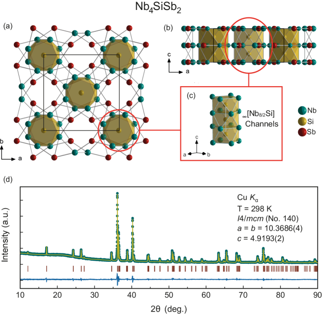
In Figure 1a and b, we present the crystal structure and the unit cell of the single-crystal refinement of \ceNb4SiSb2, shown along the c-direction and along the b-direction, respectively. The structure of \ceNb4SiSb2 was determined by means of single crystal X-Ray diffraction (SXRD) at 160 K and the elemental composition was confirmed using EDX analysis at ambient temperature (Supplementary Information).
We find \ceNb4SiSb2 to crystallize in the tetragonal space group I4/mcm with the lattice parameters a = b = 10.3638(2) Å and c = 4.9151(2) Å with the corresponding calculated cell volume of V = 527.92(3) Å3. Hence, it is found to adopt the same centrosymmetric structure type that was previously reported for \ceV4SiSb215, 16. The crystallographic data and the details of the structure refinement are summarised in Table 1. All crystallographic positions as well as the anisotropic displacement parameters are presented in Table 2.
In the structure of \ceNb4SiSb2 each atom occupies one atomic site: The niobium atoms are located at the 16k Wyckoff position, silicon occupies the 4a and antimony the 8h Wyckoff positions. Silicon forms thereby columns which can be interpreted as ∞[Nb8/2Si] chains along the c-direction as shown in Figure 1(c). The Si–Si bonding distance in \ceNb4SiSb2 within the columns is 2.4576(1) Å, which is in good agreement with the ones found in \ceV4SiSb215 and comparable to Si–Si bond distances in similar structures.26, 17 Each Si atom is surrounded by eight Nb atoms with a distance of 2.6252(6) Å forming antiprisms with the surrounding neighbour atoms. Nb has a coordination number (CN) of 13 consisting of six Nb neighbours located in the ∞[Nb8/2Si] column, one Nb in the adjacent ∞[Nb8/2Si] column, two Si, and four Sb neighbours located in between the two columns. The Nb–Nb distances range from 3.0275(8) to 3.2807(9) Å. These distances, together with the relatively short intercolumn distance between two Nb atoms of 3.0449(13) Å are in good agreement with distances found in comparable structures.27, 28 Also, the Nb–Sb distance ranging from 2.8238(7) Å to 2.9781(4) Å is in good agreement with the distances found in the related compounds, such as e.g. in \ceNb5Sb4.28 Each Sb has eight Nb neighbours and therefore a CN of 8. Another feature of this structure are the voids at the 4b Wyckoff position. These void positions are surrounded by four Sb atoms. These form void channels along the c-direction. If these void positions were fully occupied, then the \ceV4SiSb2 structure would be equivalent to the \ceW5Si3 structure.15
The validity of the structural model, the phase purity, and the homogeneity of the sample were confirmed by means of PXRD at ambient temperature and SXRD at 160 K. The reliability factors of the SXRD refinement can be found in the supplementary information. In figure 3(d) the PXRD pattern of the polycrystalline sample is shown, with its respective Rietveld refinement. We find the lattice parameters of a = b = 10.3686(4) Å , and c = 4.9193(2) Å , as well as a calculated cell volume of V = 528.86(3) Å3. Hence, the SXRD and PXRD refinements and structural solutions are in excellent agreement with each other (Supplementary Information).
3.2 Superconducting Properties of \ceNb4SiSb2
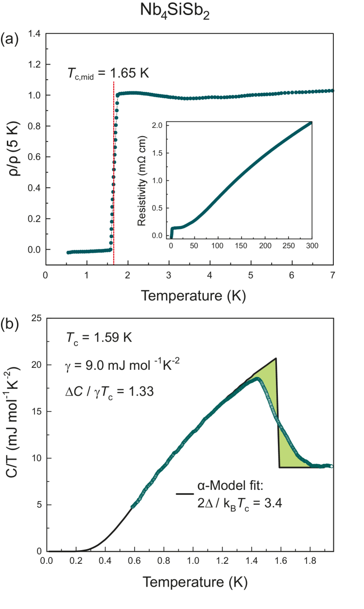
In Figure 2(a), we show the temperature-dependant resistivity of \ceNb4SiSb2 in zero field as between T = 300 K and 500 mK (inset) and in the vicinity of the superconducting transition. A sharp drop in the resistivity is observed at low temperature, corresponding to a transition to a superconducting state. The transition midpoint of K and reaches a state of zero resistance at K. The transition is comparably sharp with a transition width of K in the resistivity. The residual resistivity (1.8 K) = 0.14 m cm at 1.8 K and the room temperature resistivity value of K) = 2.06 m cm, result in a residual resistivity ratio (RRR) here defined as RRR = . This RRR value corresponds to the value of a good metal.
The bulk nature of the superconductivity in \ceNb4SiSb2 is confirmed by low-temperature specific-heat measurements. Temperature-dependent specific-heat measurements are of particular importance to prove the bulk nature of a superconductor.29, 30
In Figure 2(b), we present the temperature-dependent specific heat of \ceNb4SiSb2 in a temperature range between 600 mK and 2 K. We find a clearly pronounced discontinuity in the specific heat, resulting from the superconducting transition. The data was fitted using the -model.31, 32 Thereby, an entropy conserving construction was used to determine the critical temperature, 1.6 K. This value is in good agreement with the critical temperature from the resistivity measurement. From the -model fit, we obtained and the Sommerfeld constant of = 9.00 mJ mol-1 K-2. We find a ratio for the normalized specific-heat jump of C/ = 1.33 mJ mol-1 K-2, which confirms the bulk nature of the superconductivity, as this value is close to the weak-coupling BCS ratio of 1.43. This corresponds to a value of the superconducting gap of .
Under the assumption of a degenerate electron gas of non-interacting particles, the electronic contribution to the heat capacity in a solid at low temperatures is proportional to the density of states at the Fermi level and linear in . With the previously determined value of = 9.00 mJ mol-1 K-2, the density of states at the Fermi level can be calculated as described by F. Heiniger et al.33 according to
| (1) |
We obtain for \ceNb4SiSb2 a density of states at the Fermi level of states eV-1.
Magnetic susceptibility measurements of \ceNb4SiSb2 were conducted in the normal-state, i.e. in a temperature range between = 10 K to 300 K, in an external field of T. The observed temperature-independent positive magnetic moment corresponds to a Pauli-paramagnet (see Supplementary Information). A summary of all obtained physical parameters can be found in Table 3.
| Parameter | Units | \ceNb4SiSb2 | \ceNb4Cu_0.2SiSb2 | \ceNb4Pd_0.2SiSb2 | \ceNb4Pt_0.14SiSb2 |
| K | 1.65 | 1.16 | 0.76 | 0.84 | |
| K | 1.59 | - | - | - | |
| RRR | - | 14.96 | 4.54 | 1.56 | 1.70 |
| mJ cm | 2.06 | 0.70 | 8.46 | 2.49 | |
| mJ cm | 0.13 | 0.15 | 5.43 | 1.46 | |
| Type of magnetism | - | Pauli-paramagnetic | Pauli-paramagnetic | Pauli-paramagnetic | Pauli-paramagnetic |
| mJ mol-1 K-2 | 9.00 | 7.5 | - | ||
| - | 1.33 | 1.2 | - | ||
| meV | 0.47 | 12 | - | ||
| states eV-1 per f.u. | 3.82 | 3.18 | - |
3.3 Crystal Structures of \ceNb4Cu_0.2SiSb2, \ceNb4Pd_0.2SiSb2, and \ceNb4Pt_0.14SiSb2
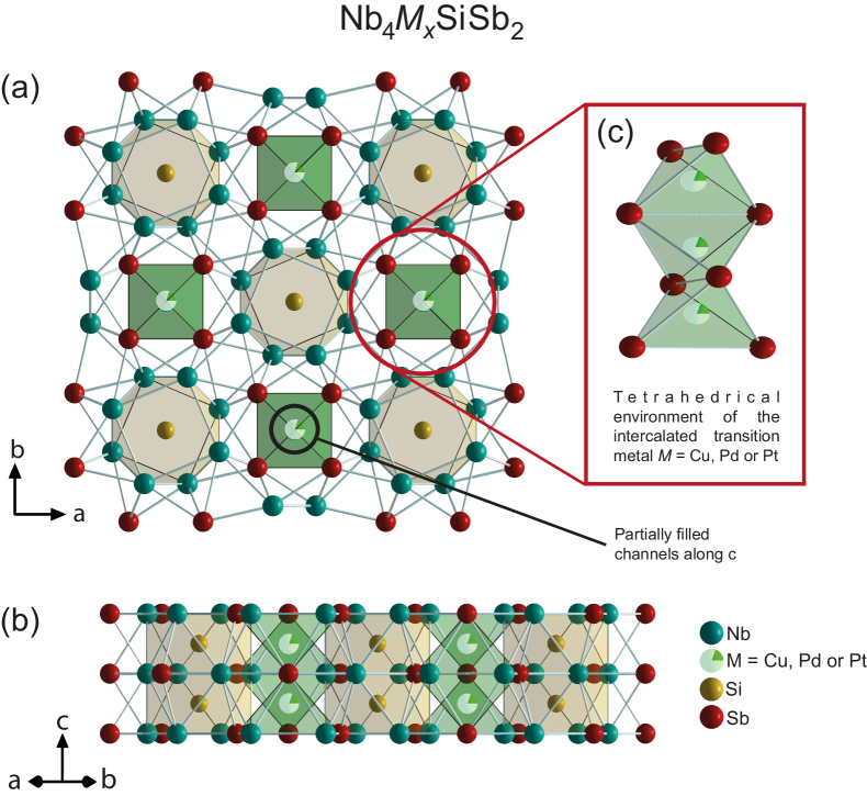
We have synthesized the three compounds \ceNb4Cu_0.2SiSb2, \ceNb4Pd_0.2SiSb2, and \ceNb4Pt_0.14SiSb2. Here, the void 4b Wyckoff positions in \ceNb4SiSb2 are partially filled with a transition metal M = Cu, Pd, or Pt, respectively. In Figure 3, we show a schematic representation of the unit cell along the c-direction and a high symmetry-direction of \ceNb4M_xSiSb2, where M = Cu, Pt and Pd with = 0.2, 0.14 and 0.2. The crystal structures of all three compounds were determined using SXRD at 160 K and PXRD diffraction at room temperature.
All samples were found to be single phase by means of PXRD measurements and corresponding Rietveld refinements (Supplementary Information). Atomic compositions were confirmed using EDX analysis (Supplementary Information).
All three structures are in good agreement with the previously reported structure for \ceNb4Pd_0.5ZSb2 with Z = Cr, Fe, Co, Ni, Si, where it was thought that a half-occupied Pd 4b site was necessary to stabilize these compounds.17 In contrary to this previous assumption, we found here that the channels were in our case either unoccupied or filled with 0.2 or 0.14 respectively (in case of Pt), independent of the initially used starting stoichiometry. These results indicate that, with improved synthesis methodologies, the continuous solid solution might be accessible in the future. All information regarding the lattice parameters, crystallographic data, and details of the structure refinements are summarized in Table 1.
3.4 Electronic Properties of \ceNb4Cu_0.2SiSb2, \ceNb4Pd_0.2SiSb2 and \ceNb4Pt_0.14SiSb2
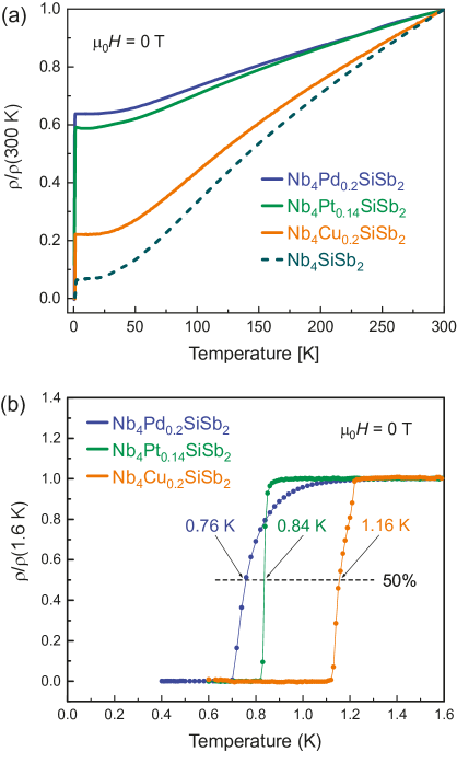
In Figure 4 we present the temperature-dependent resistivity and the normalized low-temperature resistivity in a temperature range between = 400 mK and 1.6 K for \ceNb4Cu_0.2SiSb2, \ceNb4Pd_0.2SiSb2 and \ceNb4Pt_0.14SiSb2, measured in zero field .
We find all three compounds to undergo a transition to a superconducting state at low temperatures. The critical temperature midpoints are determined as K for \ceNb4Cu_0.2SiSb2, K for \ceNb4Pd_0.2SiSb2 and K for \ceNb4Pt_0.14SiSb2. All three compounds with atoms in the void position of \ceNb4SiSb2 have lower transition temperatures than the parent compound.
For comparison, we have performed specific heat measurements in the normal state of \ceNb4SiSb2 and \ceNb4Pt_0.14SiSb2 (shown in the SI). For \ceNb4SiSb2 we find values for and of 8.40 mJ mol-1 K-2 and 0.16 mJ mol-1 K-4, respectively. The value of this fit is in good agreement with the more accurate low-temperature value discussed above. For \ceNb4Pt_0.14SiSb2 we find values for and of 9.10 mJ mol-1 K-2 and 0.31 mJ mol-1 K-4, respectively. We note that the values for differ only slightly, indicating a small change of the electronic properties upon void position filling. We find, however, that changes quite strongly. These findings indicate that the decrease of the superconducting transition temperature is likely caused by a change in the phonons, and the vibrations, respectively.
Nb4Pd_0.2SiSb2 has the lowest critical temperature of the doped compounds, as well as the lowest RRR value of RRR = . \ceNb4Cu_0.2SiSb2 with RRR = 4.54 and \ceNb4Pt_0.14SiSb2 with RRR = 1.70 follow the descending trend observed for the critical temperatures accordingly. These low RRR values correspond to a poor metallic behaviour and are 3 to 24 times smaller than the RRR of the parent compound \ceNb4SiSb2. The pronounced effect on the physical properties on void position doping becomes clearly apparent in the large change of the RRR values. The nature of the change is, however, not only affected by the electronic states, but also by the phonons and by impurity state scattering.
4 Conclusion
We have reported on the discovery of the centrosymmetric structure compound \ceNb4SiSb2. This phase was found to crystallize in the tetragonal \ceV4SiSb2-type structure. We found \ceNb4SiSb2 to undergo a transition to a superconducting state at a critical temperature of . The bulk nature of the superconducting transition was evidenced by a clear discontinuity in specific heat, with a normalized specific heat jump of 1.33 mJ mol-1 K-2, close to the weak-coupling BCS value. Furthermore, we have shown that the unoccupied 4b Wyckoff site in \ceNb4SiSb2 can be partially occupied with the transition metals Cu, Pd, or Pt.
These compounds crystallize in a tetragonal variant of the \ceW5Si3-type structure with partially occupied channels, extending along the c-direction. All three compounds were found to be superconductors with transitions temperatures of for \ceNb4Cu_0.2SiSb2, for \ceNb4Pd_0.2SiSb2 and for \ceNb4Pt_0.14SiSb2. We find that the insertion of a host atom into the void positions strongly affects the electronic and superconducting properties of this material.
Hence, our results indicate that this and related compounds might be promising host structures for the discovery of new superconducting materials, as they allow for a controlled manipulation of the electronic and phononic properties by chemical manipulation.
Conflicts of Interest
There are no conflicts to declare.
Acknowledgements
This work was supported by the Swiss National Science Foundation under Grant No. PCEFP2_194183 and by grants from the Research Grants Council of the Hong Kong Special Administrative Region, China (GRF-16302018 & C6025-19G-A).
Notes and references
- Yazici et al. 2013 D. Yazici, K. Huang, B. D. White, I. Jeon, V. W. Burnett, A. J. Friedman, I. K. Lum, M. Nallaiyan, S. Spagna and M. B. Maple, Phys. Rev. B - Condens. Matter Mater. Phys., 2013, B 87, 1–8.
- Zhang et al. 2017 Y. Zhang, B. Wang, Z. Xiao, Y. Lu, T. Kamiya, Y. Uwatoko, H. Kageyama and H. Hosono, npj Quantum Mater., 2017, 2, 45.
- Akimitsu 2019 J. Akimitsu, Proc. Jpn. Acad. Ser. B Phys. Biol. Sci., 2019, 95, 321–342.
- Ma et al. 2021 K. Ma, K. Gornicka, R. Lefèvre, Y. Yang, H. M. Rønnow, H. O. Jeschke, T. Klimczuk and F. O. von Rohr, ACS Mater. Au, 2021, 1, 55–61.
- Wang et al. 2019 B. Wang, Y. Zhang, S. Xu, K. Ishigaki, K. Matsubayashi, J.-G. Cheng, H. Hosono and Y. Uwatoko, Chin. Physics B, 2019, 28, 107401.
- Bortolozo et al. 2012 A. D. Bortolozo, C. A. Dos Santos, R. F. Jardim, C. Ritter, A. Devishvili, M. Rotter, F. G. Gandra and A. J. MacHado, J. Appl. Phys., 2012, 111, 1–6.
- Ma et al. 2021 K. Ma, R. Lefèvre, K. Gornicka, H. O. Jeschke, X. Zhang, Z. Guguchia, T. Klimczuk and F. O. von Rohr, Chem. Mater., 2021, 33, 8722–8732.
- Aronsson et al. 1955 B. Aronsson, O. Tjomsland, R. Lundén and H. Prydz, Acta Chem. Scand., 1955, 9, 1107–1110.
- Kawashima et al. 2009 K. Kawashima, T. Muranaka, Y. Kousaka, S. Akutagawa and J. Akimitsu, J. Phys. Conf. Ser., 2009, 150, 1–4.
- Willis 1979 J. O. Willis, J. Appl. Phys., 1979, 50, 2863–2865.
- Shishido et al. 1989 T. Shishido, K. Ukei, N. Toyota, T. Sasaki, Y. Watanabe, K. Motai, T. Fukuda, H. Takeya and H. Takei, J. Cryst. Growth, 1989, 96, 1–6.
- Shishido et al. 1989 T. Shishido, J. Ye, N. Toyota, K. Ukei, T. Sasaki, H. Horiuchi and T. Fukuda, Jpn. J. Appl. Phys., 1989, 28, 1519–1520.
- Xie et al. 2015 W. Xie, H. Luo, B. F. Phelan and R. J. Cava, J. Mater. Chem. C, 2015, 3, 8235–8240.
- Rytz and Hoffmann 1999 R. Rytz and R. Hoffmann, Inorg. Chem., 1999, 38, 1609–1617.
- Wollesen and Jeitschko 1996 P. Wollesen and W. Jeitschko, J. Alloys Compd., 1996, 243, 67–69.
- Richter et al. 1997 G. C. Richter, W. Jeitschko, B. Künnen and H. M. Gerdes, Inorg. Chem., 1997, 133, 400–406.
- Wang et al. 2001 M. Wang, W. C. Sheets, R. McDonald and A. Mar, Inorg. Chem., 2001, 40, 5199–5205.
- Clark and Reid 1995 R. Clark and J. Reid, Acta Crystallographica Section A: Foundations of Crystallography, 1995, 51, 887–897.
- Dolomanov et al. 2009 O. V. Dolomanov, L. J. Bourhis, R. J. Gildea, J. A. Howard and H. Puschmann, Journal of applied crystallography, 2009, 42, 339–341.
- Sheldrick 2015 G. M. Sheldrick, Acta Crystallographica Section A: Foundations and Advances, 2015, 71, 3–8.
- Sheldrick 2015 G. M. Sheldrick, Acta Crystallographica Section C: Structural Chemistry, 2015, 71, 3–8.
- Spek 2009 A. L. Spek, Acta Crystallographica Section D: Biological Crystallography, 2009, 65, 148–155.
- Rodríguez-Carvajal 1993 J. Rodríguez-Carvajal, Physica B: Condensed Matter, 1993, 192, 55–69.
- Finger et al. 1994 L. Finger, D. Cox and A. Jephcoat, Journal of applied Crystallography, 1994, 27, 892–900.
- Mak et al. 2013 H. K. Mak, P. Burger, L. Cevey, T. Wolf, C. Meingast and R. Lortz, Phys. Rev. B Condens. Matter, 2013, 87, 214523.
- Badding and DiSalvo 1990 M. E. Badding and F. J. DiSalvo, Inorg. Chem., 1990, 29, 3952–3954.
- Janger and Rasmussen 1975 S. Janger and S. E. Rasmussen, Acta Crystallogr., 1975, B31, 2881 – 2883.
- Lomnytska and Kuz’ma 2006 Y. F. Lomnytska and Y. B. Kuz’ma, J. Alloys Compd., 2006, 413, 114–117.
- Carnicom et al. 2019 E. M. Carnicom, W. Xie, Z. Yang, K. Górnicka, T. Kong, T. Klimczuk and R. J. Cava, Chem. Mater., 2019, 31, 2164–2173.
- Witteveen et al. 2021 C. Witteveen, K. Górnicka, J. Chang, M. Månsson, T. Klimczuk and F. O. von Rohr, Dalt. Trans., 2021, 50, 3216–3223.
- Padamsee et al. 1973 H. Padamsee, J. E. Neighbor and C. A. Shiffman, J. Low Temp. Phys., 1973, 12, 387–411.
- Johnston 2013 D. C. Johnston, Supercond. Sci. Technol., 2013, 26, 1–19.
- Heiniger et al. 1966 F. Heiniger, E. Bucher and J. Muller, Phys. der Kondens. Mater., 1966, 5, 243–284.