Impact of disorder on the distribution of gate coupling strengths in a spin qubit device
Sathish R. Kuppuswamy1*, Hugo Kerstens1, Chun-Xiao Liu1, 2, Lin Wang1 and Anton Akhmerov1
1 Kavli Institute of Nanoscience, Delft University of Technology, Delft 2600 GA, The Netherlands
2 Qutech, Delft University of Technology, Delft 2600 GA, The Netherlands
* rksathish09@gmail.com
Abstract
A scalable spin-based quantum processor requires a suitable semiconductor heterostructure and a gate design, with multiple alternatives being investigated. Characterizing such devices experimentally is a demanding task, with the full development cycle taking at least months. While numerical simulations are more time-efficient, their predictive power is limited due to unavoidable disorder and device-to-device variation. We develop a spin-qubit device simulation for determining the distribution of the coupling strengths between the electrostatic gate potentials and the effective device Hamiltonian in presence of disorder. By comparing our simulation results with the experimental data, we demonstrate that the coupling of the gate voltages to the dot chemical potential and the interdot tunnel coupling match up to disorder-induced variance. To demonstrate the flexibility of our approach, we also analyze an alternative non-planar geometry inspired by FinFET devices.
1 Introduction
Spin qubits are an actively developed platform for building a quantum computer with both single- and two-qubit gate fidelity exceeding the error threshold required for achieving fault tolerance [1, 2, 3]. In general, this approach follows the Loss and DiVincenzo proposal [4] and traps single electrons in an array of coupled quantum dots. Time-dependent manipulation of chemical potentials and quantum dot couplings using plunger and barrier electrostatic gates implements coherent operations on the electron spins—the quantum gates [5]. Prototype implementations of a few quantum dot devices were demonstrated in several material platforms, for example in \ceGaAs [6, 5, 7, 8], \ceSi/SiGe [9, 10, 11, 12], \ceGe/SiGe [13, 14] and \ceSi/SiO_2 [15, 16, 17] heterostructures.
To go beyond a few qubit devices, the ongoing effort is invested into designing and operating larger-scale quantum dot arrays [8, 12, 18] necessary to implement more complex quantum circuits without compromising qubit performance. For example, the change from \ceGaAs to \ceSi avoids decoherence due to the hyperfine coupling to the nuclear spins [19]. Because the electron effective mass is larger in \ceSi, the electrostatic gates must be smaller and closer to each other due to the higher electron localization [11, 12]. Another ongoing development—2D quantum dot arrays [14, 8]—improves qubit connectivity, and more directly corresponds to the error correcting codes. Although such new designs are vital for future progress, they require going beyond the state of the art in device complexity and precision.
Spin qubit gate designs are commonly characterized by performing the full experimental cycle: fabricating, tuning, and then measuring the device. This pipeline can be partially tested using numerical simulations [20]. Numerical simulations begin with discretizing the continuum Hamiltonian which describes the two-dimensional (2DEG) electron gas in a semiconductor heterostructure. The potential landscape of the 2DEG is shaped to host quantum dots by optimizing the electrostatic environment using non-linear optimizers. In this process, electrostatic potential due to gates is calculated by solving Poisson’s equation. Finally, the discretized Hamiltonian is diagonalized to obtain eigenenergies and eigenvectors of the electron states confined in quantum dots. Numerical simulations, despite being complex and demanding, require not longer than days to run, and therefore they are still much faster than fabrication and measurement that lasts months.
Structural variation due to the fabrication as well as electrostatic disorder [21, 22] limits the usefulness of numerical simulations. In addition, although gates are designed to predominantly control only one parameter, changing the voltage of one plunger or barrier gate affects all the dot Hamiltonian parameters instead of a single chemical potential or a tunnel coupling [23]. Because of these complications, a significant amount of effort is dedicated to automating the tuning of an experimental device using either an effective model combined with a measurement protocol [23] or using a more general machine learning techniques [24, 25, 26, 27].
The final tuning step determines the virtual gates [23]—linear combinations of physical gates that couple to a single quantum dot Hamiltonian parameter—that enable efficient time-dependent manipulation of spin qubit devices [28]. Here we demonstrate that such gate coupling strengths are efficiently predicted by numerical simulations even in the presence of disorder. We also provide a reference implementation for performing this procedure, available at [29]. Our simulation of an experimental device agrees with the measurements up to the expected uncertainty due to electrostatic disorder. We also demonstrate the flexibility of our approach by applying it to a non-planar geometry inspired by a FinFET transistor setup [17, 30]. Furthermore, by implementing relevant optimizations, we can reduce the simulation time of a single device to a few minutes of CPU time.
2 Methods
In the continuum approximation, the Hamiltonian of the 2DEG confined in a semiconductor heterostructure is
| (1) |
where is the effective mass and is the gate-defined electrostatic potential. We ignore the spin degree of freedom in this work and only focus on finding the relation between gate potential and electrostatic potential of the 2DEG in the presence of disorder. We further discretize Eq. (1) on a two-dimensional regular grid with nearest-neighbor hoppings to form the tight-binding Hamiltonian H.
Electrostatic potential is a solution to the Poisson’s equation
| (2) |
where is the vacuum permittivity, and is the relative permittivity. We apply Dirichlet boundary conditions with potential at the -th gate electrode boundary and at the simulation boundary. The source term is the charge density which only includes the possible impurity charges
| (3) |
where the summation is carried out over all the positions of the charged impurities, and is the elementary charge. Because we are interested in the single particle Hamiltonian, we neglect the interaction of electrons in different quantum dots, which can be added at later steps. This makes the Poisson equation linear. To reduce the finite-size effects, we simulate a sufficiently large volume surrounding the sample. We use the electrostatic solver of Ref. [31] to construct the finite volume mesh of the simulation area and solve the discretized Poisson equation. To improve performance, we use a coarser grid in the empty space. The general solution of Eq. (2) is
| (4) |
where is the solution with all , and is the solution with and the Kronecker symbol. Recasting the solution in this form allows us to compute the LU-decomposition of the Laplace operator once, and apply it only once per gate electrode and impurity charge distribution.
We transform the lowest few eigenstates of H that correspond to the ground state of each dot into a maximally localized form along x with the projected position operator
| (5) |
where , with N the number of quantum dots. The matrix diagonalizing is the transformation to the basis of the Wannier orbitals maximally localized in the -direction, with the eigenvalues of being the Wannier centers—the expected -positions of these orbitals. We compute the effective Hamiltonian for the quantum dots in the basis of Wannier functions using
| (6) |
where is a diagonal matrix with lowest eigenvalues of H. Reformulating the Hamiltonian into the sum of a constant term and the term which changes as a function of the gate k
| (7) |
allows us to compute the onsite and off-diagonal elements of as a function of the gate voltages
| (8) | ||||
where is the chemical potential of dot and is the tunnel coupling between the nearest-neighboring dots and . The partial derivatives and are the coupling strengths between the -th gate and the -th chemical potential and the -th interdot tunnel coupling respectively.
To tune the device into the optimal operating region, we numerically optimize the gate voltages to trap a single electron state in each quantum dot and to set all interdot couplings to the same value. We achieve this result using the cost function
| (9) |
where is the desired chemical potential and is the desired interdot tunnel coupling. Since varies exponentially as a function of the barrier height [28], we apply the natural logarithm to the tunnel couplings in Eq. (9), to make the relative significance of two contributions to the cost function comparable.
In presence of charge impurities in concentrations expected in realistic devices, the optimization using the cost function of Eq. (9) fails to tune the device into the proper tunneling regime or even form quantum dots due to the highly nonlinear nature of the problem. To enable convergence in the presence of disorder we add the disorder potential with a Lagrange multiplier to Eq. (7) and add to the cost function. In addition, we optimize dots to be confined to the specific regions by using soft thresholds
| (10) |
where is the desired range. Combining all terms, we end up with the regularized cost function
| (11) |
with the -coordinate of the -th Wannier orbital, is the desired position of the -th dot center, and , the dot position tolerance. Optimizing has a high success rate and converges close to the tuned point in the majority of cases. We follow the optimization of with an additional optimization of to ensure that the final configuration corresponds to .
3 Results
3.1 Planar geometry
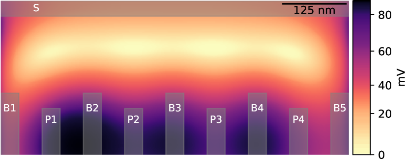
We benchmark the numerical simulations by comparing them with the measured data of silicon-doped \ceGaAs/AlGaAs heterostructure measured in Ref. [28]. This device consists of a 2DEG with the dopant density . We approximate the electron density of the undepleted 2DEG—the region away from the dots and the gates—to be equal to the dopant density. Plunger and barrier gates are deposited at above the 2DEG to selectively deplete the 2DEG and form quantum dots. Plunger gates mainly couple to , while barrier gates control . Following Ref. [28] we consider four plunger gates (P1 to P4) and five barrier gates (B1 to B5) to form an array of four quantum dots. We numerically optimize the gate voltages to trap a single electron in each quantum dot and tune to the experimental operating point. The 2DEG electrostatic potential of a tuned clean device is shown in Fig. 1.
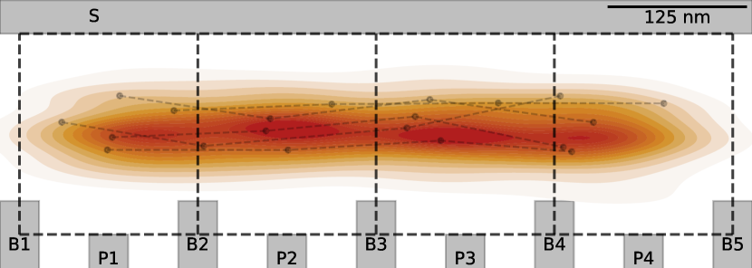
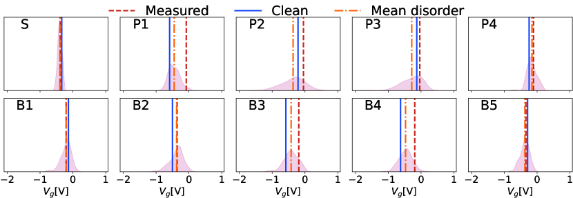
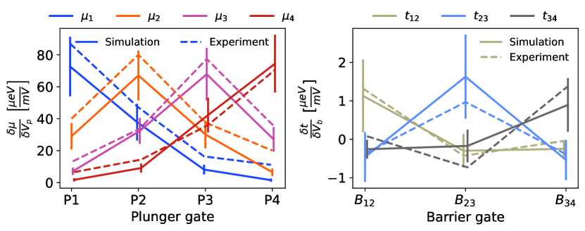
Following the analysis of Ref. [32], we focus on the dopant charge distribution as the main source of disorder. We simulate the dopants by making the charge of the mesh volumes in the dopant layer Poisson-distributed random variables with the average charge density equal to the dopant density and consider 200 disorder realizations. The target Hamiltonian for the optimization has (assuming the Fermi energy in the 2DEG is at ) and all the interdot couplings are set to . The optimization converges to the desired result in 65% of disorder realizations. While it is likely that further improvements to the optimization algorithm would increase the convergence rate, we consider this performance sufficient since we expect that this value is higher than the experimental yield—the percentage of devices that could be tuned to the proper operating regime compared to the total number of devices attempted in the experiments. The positions of the dot centers in the converged samples exhibit a variation comparable to the dot size, as shown in Fig. 2. We benchmark our numerical simulations by comparing the gate voltages and the gate coupling strengths with the experimentally measured ones in Fig. 3 and Fig. 4 respectively. While the operating point varies strongly across disorder realizations, we find that most measured gate coupling strengths and gate voltages lie within the standard deviation of the computed ones.
3.2 Non-planar geometry
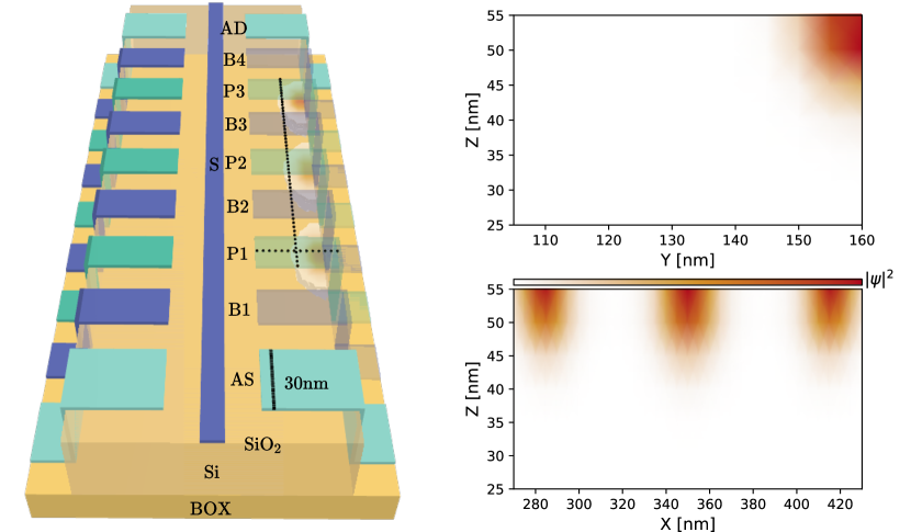
To demonstrate the universality of our approach, we calculate the gate coupling strengths in a non-planar geometry. We consider the Si-heterostructure from Ref. [30, 17]. This device consists of a slab of \ceSi grown on an insulator as shown in Fig. 5. The \ceSi is surrounded by \ceSiO_2 on the four faces with plunger and barrier gates deposited on the top, right, and left faces. We tune the gates on one side of the device to form quantum dots underneath. The other side is used for sensing and plays no role in our simulations. Similar to the planar geometry, the plunger gates P1, P2, and P3 control the dot occupation, while the barrier gates B2 and B3 tune the tunnel barrier strengths. We apply the optimization procedure of Sec. 2 to tune the device to its operating point. Due to the device geometry, electron wave functions localize near the sample edge under the plunger gates as shown in Fig. 5.
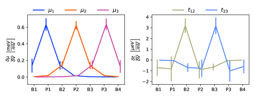
We simulate disorder in the \ceSi potential landscape by randomly distributing positive charges in \ceSiO_2 with a surface charge density of which is close to the experimentally observed value in the \ceSiO_2 [33] and We perform numerical optimization in two stages. Due to the larger effective mass in \ceSi, the tuning of the non-planar device is less stable. We resolve this by excluding the contribution of interdot coupling to in the first optimization step. In the second step, we optimize with . We repeat this process for 200 realizations of surface charge disorder. After the two-stage optimization, we compute the gate coupling strengths using Eq. (8) only for those samples for which the optimization converges with precision , and . Finally, we filter out several outlier disorder realizations with . After performing the two filtering steps, just over 50 % of realizations remain. In Fig. 6, we show the plunger and barrier gate coupling strengths to the dot chemical potential and interdot tunnel couplings for the filtered realizations. We find that due to the stronger localization of the wave functions and smaller distance between the gates and the bound states, the non-local gate couplings are strongly suppressed in the non-planar geometry, compared to the planar one.
4 Summary
We developed a software tool to predict the disorder-induced variation in spin qubit devices. Our approach relies on an automated tuning procedure able to tune devices with realistic disorder in the majority of disorder realizations to their operating point. To benchmark our result, we compared the predicted gate voltage and gate coupling strengths distributions to those measured in a \ceGaAs device and found an agreement within a standard deviation of the predicted parameters. We demonstrated that our tool also functions with a comparable efficiency when applied to a non-planar \ceSi device.
Currently, our package disregards interdot Coulomb repulsion as well as lattice strain. We expect that after extending the simulation to include these phenomena in the simulation, our approach will become sufficiently general to optimize device geometry and guide the tuning of experimentally realized devices.
Acknowledgements
We would like to thank I. Araya Day, J. David, C. J. van Diepen, T.-K. Hsiao, A. Lacerda, and S. Miles for useful discussions.
Data Availability
All code and data used in the manuscript are available at Zenodo [29].
Author contributions
S.R.K. and A.A. formulated the project goal with input from L.W.; A.A. and S.R.K. designed the project approach; S.R.K. and H.K. established electrostatic simulations with input from C.X.L.; under the supervision of A.A., S.R.K. and H.K. carried out numerical simulations of the planar and the non-planar geometry respectively; S.R.K., C.X.L., and A.A. interpreted the results; S.R.K., H.K., and A.A. wrote the manuscript with input from C.X.L. and L.W.
Funding information
This work was supported by the the Netherlands Organisation for Scientific Research (NWO/OCW) as part of the Frontiers of Nanoscience program, an ERC Starting Grant 638760, a subsidy for top consortia for knowledge and innovation (TKl toeslag) and a NWO VIDI Grant (016.Vidi.189.180).
References
- [1] D. A. Lidar and T. A. Brun, Quantum error correction (2013).
- [2] X. Xue, M. Russ, N. Samkharadze, B. Undseth, A. Sammak, G. Scappucci and L. M. K. Vandersypen, Quantum logic with spin qubits crossing the surface code threshold, Nature 601(7893), 343 (2022), 10.1038/s41586-021-04273-w.
- [3] A. Noiri, K. Takeda, T. Nakajima, T. Kobayashi, A. Sammak, G. Scappucci and S. Tarucha, Fast universal quantum gate above the fault-tolerance threshold in silicon, Nature 601(7893), 338 (2022), 10.1038/s41586-021-04182-y.
- [4] D. Loss and D. P. DiVincenzo, Quantum computation with quantum dots, Phys. Rev. A 57, 120 (1998), 10.1103/PhysRevA.57.120.
- [5] J. R. Petta, A. C. Johnson, J. M. Taylor, E. A. Laird, A. Yacoby, M. D. Lukin, C. M. Marcus, M. P. Hanson and A. C. Gossard, Coherent manipulation of coupled electron spins in semiconductor quantum dots, Science 309(5744), 2180 (2005), 10.1126/science.1116955, https://www.science.org/doi/pdf/10.1126/science.1116955.
- [6] J. M. Elzerman, R. Hanson, J. S. Greidanus, L. H. Willems van Beveren, S. De Franceschi, L. M. K. Vandersypen, S. Tarucha and L. P. Kouwenhoven, Few-electron quantum dot circuit with integrated charge read out, Phys. Rev. B 67, 161308 (2003), 10.1103/PhysRevB.67.161308.
- [7] C. Volk, A. M. J. Zwerver, U. Mukhopadhyay, P. T. Eendebak, C. J. van Diepen, J. P. Dehollain, T. Hensgens, T. Fujita, C. Reichl, W. Wegscheider and L. M. K. Vandersypen, Loading a quantum-dot based “qubyte” register, npj Quantum Information 5(1), 29 (2019), 10.1038/s41534-019-0146-y.
- [8] P.-A. Mortemousque, E. Chanrion, B. Jadot, H. Flentje, A. Ludwig, A. D. Wieck, M. Urdampilleta, C. Bäuerle and T. Meunier, Coherent control of individual electron spins in a two-dimensional quantum dot array, Nature Nanotechnology 16(3), 296 (2021), 10.1038/s41565-020-00816-w.
- [9] R. Vrijen, E. Yablonovitch, K. Wang, H. W. Jiang, A. Balandin, V. Roychowdhury, T. Mor and D. DiVincenzo, Electron-spin-resonance transistors for quantum computing in silicon-germanium heterostructures, Phys. Rev. A 62, 012306 (2000), 10.1103/PhysRevA.62.012306.
- [10] T. F. Watson, S. G. J. Philips, E. Kawakami, D. R. Ward, P. Scarlino, M. Veldhorst, D. E. Savage, M. G. Lagally, M. Friesen, S. N. Coppersmith, M. A. Eriksson and L. M. K. Vandersypen, A programmable two-qubit quantum processor in silicon, Nature 555(7698), 633 (2018), 10.1038/nature25766.
- [11] D. M. Zajac, T. M. Hazard, X. Mi, K. Wang and J. R. Petta, A reconfigurable gate architecture for Si/SiGe quantum dots, Applied Physics Letters 106(22), 223507 (2015), 10.1063/1.4922249.
- [12] D. M. Zajac, T. M. Hazard, X. Mi, E. Nielsen and J. R. Petta, Scalable gate architecture for a one-dimensional array of semiconductor spin qubits, Phys. Rev. Applied 6, 054013 (2016), 10.1103/PhysRevApplied.6.054013.
- [13] N. W. Hendrickx, D. P. Franke, A. Sammak, G. Scappucci and M. Veldhorst, Fast two-qubit logic with holes in germanium, Nature 577(7791), 487 (2020), 10.1038/s41586-019-1919-3.
- [14] W. I. L. Lawrie, H. G. J. Eenink, N. W. Hendrickx, J. M. Boter, L. Petit, S. V. Amitonov, M. Lodari, B. Paquelet Wuetz, C. Volk, S. G. J. Philips, G. Droulers, N. Kalhor et al., Quantum dot arrays in silicon and germanium, Applied Physics Letters 116(8), 080501 (2020), 10.1063/5.0002013, https://doi.org/10.1063/5.0002013.
- [15] W. H. Lim, H. Huebl, L. H. Willems van Beveren, S. Rubanov, P. G. Spizzirri, S. J. Angus, R. G. Clark and A. S. Dzurak, Electrostatically defined few-electron double quantum dot in silicon, Applied Physics Letters 94(17), 173502 (2009), 10.1063/1.3124242, https://doi.org/10.1063/1.3124242.
- [16] M. Veldhorst, C. H. Yang, J. C. C. Hwang, W. Huang, J. P. Dehollain, J. T. Muhonen, S. Simmons, A. Laucht, F. E. Hudson, K. M. Itoh, A. Morello and A. S. Dzurak, A two-qubit logic gate in silicon, Nature 526(7573), 410 (2015), 10.1038/nature15263.
- [17] W. Gilbert, A. Saraiva, W. H. Lim, C. H. Yang, A. Laucht, B. Bertrand, N. Rambal, L. Hutin, C. C. Escott, M. Vinet and A. S. Dzurak, Single-electron operation of a silicon-CMOS quantum dot array with integrated charge sensing, Nano Letters 20(11), 7882 (2020), 10.1021/acs.nanolett.0c02397.
- [18] A. M. J. Zwerver, T. Krähenmann, T. F. Watson, L. Lampert, H. C. George, R. Pillarisetty, S. A. Bojarski, P. Amin, S. V. Amitonov, J. M. Boter, R. Caudillo, D. Corras-Serrano et al., Qubits made by advanced semiconductor manufacturing (2021), 2101.12650.
- [19] B. M. Maune, M. G. Borselli, B. Huang, T. D. Ladd, P. W. Deelman, K. S. Holabird, A. A. Kiselev, I. Alvarado-Rodriguez, R. S. Ross, A. E. Schmitz, M. Sokolich, C. A. Watson et al., Coherent singlet-triplet oscillations in a silicon-based double quantum dot, Nature 481(7381), 344 (2012), 10.1038/nature10707.
- [20] X. Gao, E. Nielsen, R. P. Muller, R. W. Young, A. G. Salinger, N. C. Bishop, M. P. Lilly and M. S. Carroll, Quantum computer aided design simulation and optimization of semiconductor quantum dots, Journal of Applied Physics 114(16), 164302 (2013), 10.1063/1.4825209, https://doi.org/10.1063/1.4825209.
- [21] D. Sabbagh, N. Thomas, J. Torres, R. Pillarisetty, P. Amin, H. George, K. Singh, A. Budrevich, M. Robinson, D. Merrill, L. Ross, J. Roberts et al., Quantum transport properties of industrial , Phys. Rev. Applied 12, 014013 (2019), 10.1103/PhysRevApplied.12.014013.
- [22] E. P. Nordberg, G. A. T. Eyck, H. L. Stalford, R. P. Muller, R. W. Young, K. Eng, L. A. Tracy, K. D. Childs, J. R. Wendt, R. K. Grubbs, J. Stevens, M. P. Lilly et al., Enhancement-mode double-top-gated metal-oxide-semiconductor nanostructures with tunable lateral geometry, Phys. Rev. B 80, 115331 (2009), 10.1103/PhysRevB.80.115331.
- [23] C. J. van Diepen, P. T. Eendebak, B. T. Buijtendorp, U. Mukhopadhyay, T. Fujita, C. Reichl, W. Wegscheider and L. M. K. Vandersypen, Automated tuning of inter-dot tunnel coupling in double quantum dots, Applied Physics Letters 113(3), 033101 (2018), 10.1063/1.5031034, https://doi.org/10.1063/1.5031034.
- [24] H. Moon, D. T. Lennon, J. Kirkpatrick, N. M. van Esbroeck, L. C. Camenzind, L. Yu, F. Vigneau, D. M. Zumbühl, G. A. D. Briggs, M. A. Osborne, D. Sejdinovic, E. A. Laird et al., Machine learning enables completely automatic tuning of a quantum device faster than human experts, Nature Communications 11(1), 4161 (2020), 10.1038/s41467-020-17835-9.
- [25] N. M. van Esbroeck, D. T. Lennon, H. Moon, V. Nguyen, F. Vigneau, L. C. Camenzind, L. Yu, D. M. Zumbühl, G. A. D. Briggs, D. Sejdinovic and N. Ares, Quantum device fine-tuning using unsupervised embedding learning, New Journal of Physics 22(9), 095003 (2020), 10.1088/1367-2630/abb64c.
- [26] J. D. Teske, S. S. Humpohl, R. Otten, P. Bethke, P. Cerfontaine, J. Dedden, A. Ludwig, A. D. Wieck and H. Bluhm, A machine learning approach for automated fine-tuning of semiconductor spin qubits, Applied Physics Letters 114(13), 133102 (2019), 10.1063/1.5088412, https://doi.org/10.1063/1.5088412.
- [27] O. Krause, A. Chatterjee, F. Kuemmeth and E. van Nieuwenburg, Learning Coulomb diamonds in large quantum dot arrays, 10.48550/ARXIV.2205.01443 (2022).
- [28] T.-K. Hsiao, C. van Diepen, U. Mukhopadhyay, C. Reichl, W. Wegscheider and L. Vandersypen, Efficient orthogonal control of tunnel couplings in a quantum dot array, Phys. Rev. Applied 13, 054018 (2020), 10.1103/PhysRevApplied.13.054018.
- [29] S. R. Kuppuswamy, H. Kerstens, L. Wang, C.-X. Liu and A. Akhmerov, Impact of disorder on the distribution of gate coupling strengths in a spin qubit device, 10.5281/zenodo.4421028 (2022).
- [30] E. Chanrion, D. J. Niegemann, B. Bertrand, C. Spence, B. Jadot, J. Li, P.-A. Mortemousque, L. Hutin, R. Maurand, X. Jehl, M. Sanquer, S. De Franceschi et al., Charge detection in an array of CMOS quantum dots, Phys. Rev. Applied 14, 024066 (2020), 10.1103/PhysRevApplied.14.024066.
- [31] P. Armagnat, A. Lacerda-Santos, B. Rossignol, C. Groth and X. Waintal, The self-consistent quantum-electrostatic problem in strongly non-linear regime, SciPost Physics 7(3) (2019), 10.21468/scipostphys.7.3.031.
- [32] P. Barthelemy and L. M. K. Vandersypen, Quantum dot systems: a versatile platform for quantum simulations, Annalen der Physik 525(10-11), 808 (2013), 10.1002/andp.201300124, https://onlinelibrary.wiley.com/doi/pdf/10.1002/andp.201300124.
- [33] H. Roh, H.-L. Kim, K. Khumaini, H. Son, D. Shin and W.-J. Lee, Effect of deposition temperature and surface reactions in atomic layer deposition of silicon oxide using bis(diethylamino)silane and ozone, Applied Surface Science 571, 151231 (2022), https://doi.org/10.1016/j.apsusc.2021.151231.