Qubits made by advanced semiconductor manufacturing
Abstract
1 QuTech and Kavli Institute of Nanoscience, Delft University of Technology, 2600 GA Delft, The Netherlands
2 Intel Components Research, Intel Corporation, 2501 NW 229th Avenue, Hillsboro, OR, USA
∗ Corresponding authors: l.m.k.vandersypen@tudelft.nl; james.s.clarke@intel.com
Full-scale quantum computers require the integration of millions of quantum bits campbell_roads_2017 ; wecker_gate-count_2014 . The promise of leveraging industrial semiconductor manufacturing to meet this requirement has fueled the pursuit of quantum computing in silicon quantum dots. However, to date, their fabrication has relied on electron-beam lithography veldhorst_addressable_2014 ; maurand_cmos_2016 ; petit_spin_2018 ; yang_operation_2020 ; harvey-collard_spin-orbit_2019 ; xue_benchmarking_2019 ; yoneda_quantum-dot_2018 ; watson_programmable_2018 ; zajac_resonantly_2018 ; andrews_quantifying_2019 ; wu_two-axis_2014 ; li_flexible_2020 and, with few exceptions maurand_cmos_2016 ; harvey-collard_spin-orbit_2019 ; li_flexible_2020 , on academic style lift-off processes. Although these fabrication techniques offer process flexibility, they suffer from low yield and poor uniformity. An important question is whether the processing conditions developed in the manufacturing fab environment to enable high yield, throughput, and uniformity of transistors are suitable for quantum dot arrays and do not compromise the delicate qubit properties. Here, we demonstrate quantum dots hosted at a 28Si/28SiO2 interface, fabricated in a 300 mm semiconductor manufacturing facility using all-optical lithography and fully industrial processing pillarisetty_qubit_2018 . As a result, we achieve nanoscale gate patterns with remarkable homogeneity. The quantum dots are well-behaved in the multi-electron regime, with excellent tunnel barrier control, a crucial feature for fault-tolerant two-qubit gates. Single-spin qubit operation using magnetic resonance reveals relaxation times of over s at Tesla and coherence times of over ms, matching the quality of silicon spin qubits reported to date veldhorst_addressable_2014 ; maurand_cmos_2016 ; harvey-collard_spin-orbit_2019 ; petit_spin_2018 ; yang_operation_2020 ; xue_benchmarking_2019 ; yoneda_quantum-dot_2018 ; watson_programmable_2018 ; zajac_resonantly_2018 ; andrews_quantifying_2019 ; wu_two-axis_2014 . The feasibility of high-quality qubits made with fully-industrial techniques strongly enhances the prospects of a large-scale quantum computer.
The idea of exploiting quantum mechanics to build computers with computational powers beyond the abilities of any classical device has gathered momentum since the 1980’s feynman_simulating_nodate . However, in order for full-fledged quantum computers to become a reality, they need to be fault-tolerant, i.e. errors from unavoidable decoherence must be reversed faster than they occur campbell_roads_2017 . The most promising architectures require a scalable qubit system of individually-addressable qubits with a gate fidelity over and tunable nearest-neighbour couplings bravyi_quantum_1998 ; fowler_surface_2012 .
Spin qubits in gate-defined quantum dots (QDs) offer great potential for quantum computation due to their small size and relatively long coherence times loss_quantum_1998 ; zwanenburg_silicon_2013 ; vandersypen_quantum_2019 . Single-qubit gate fidelities over 99.9% yoneda_quantum-dot_2018 ; yang_silicon_2019 as well as two-qubit gates veldhorst_two-qubit_2015 ; zajac_resonantly_2018 ; huang_fidelity_2019 ; xue_benchmarking_2019 ; hendrickx_fast_2020 , algorithms watson_programmable_2018 , conditional teleportation qiao_conditional_2020 , three-qubit entanglement takeda_quantum_nodate and four-qubit universal control hendrickx_four-qubit_2020 have already been demonstrated. Moreover, silicon spin qubits have been operated at relatively high temperatures of 1-4 K petit_universal_2020 ; yang_operation_2020 , where the higher cooling power enables scaling strategies with integration of control electronics vandersypen_interfacing_2017 ; veldhorst_silicon_2017 ; li_crossbar_2018 ; pauka_cryogenic_2019 ; xue_cmos-based_2020 .
A major advantage of silicon spin qubits is that they could leverage decades of technology development in the semiconductor industry. Today, industry is able to make uniform transistors with gate lengths of several tens of nanometers and spaced apart by nm (fins) to nm (gates), feature sizes that are well below the nm wavelength of the light used in the lithography process auth2017 . This engineering feat and the high yield that allows integrated circuits containing billions of transistors to function, are enabled by adhering to strict design rules and by advanced semiconductor manufacturing techniques such as multiple patterning for pitch doubling, subtractive processing, chemically-selective plasma etches, and chemical mechanical polishing (CMP) zant2014 . While these processing conditions are more intrusive than the metal lift-off processing conditions typically used on academic devices, they will be key to achieving the extremely high yield necessary for the fabrication of thousands or millions of qubits in a functional array.
A quantum dot device bears a strong similarity to a transistor, taken to the limit where the gate above the channel controls the flow of electrons one at a time averin86 . In linear qubit arrays, the transistor gate is replaced by multiple gates, used to shape the potential landscape of the channel into multiple potential minima (quantum dots), to control the occupation of each dot down to the last electron, and to precisely tune the wavefunction overlap (tunnel coupling) of electrons in neighbouring dots van_der_wiel_electron_2002 . In addition, qubit devices commonly rely on integrated nearby charge sensors to enable single-shot spin readout and high-fidelity initialisation hanson_spins_2007 ; vandersypen_quantum_2019 . A first key question is then whether the reliable but strict design rules of industrial patterning can produce suitable qubit device layouts. A separate consideration is that qubit coherence is easily affected by microscopic charge fluctuations from interface, surface and bulk defects. Therefore, a second key question is whether the coherence properties of the qubits survive the processing conditions needed to achieve high yield and uniformity. Although the first qubits in quantum dots fabricated on wafer-scale in industrial foundries have been presented maurand_cmos_2016 ; chanrion_charge_2020 , they rely on electron-beam lithography and avoid CMP for the active device area. CMP requires a uniform metal density across the wafer, which introduces its own complexities for quantum dot devices, due to the large amount of floating metal and added capacitance.
In this letter, we demonstrate optically-patterned quantum dots and qubits, made in a state-of-the-art 300 mm wafer process line, similar to those used for commercial advanced integrated circuits.
A dedicated mask set based on 193 nm immersion lithography is created for patterning quantum dot arrays of various lengths, as well as a number of test structures, such as transistors of various sizes and Hall bars. These test structures allow us to directly extract important metrics at both room temperature and low temperature such as mobility, threshold voltage, subthreshold slope and interface trap density. Analysed together, these metrics give us understanding of the gate oxide and contact quality along with the electrostatics to help troubleshoot process targeting pillarisetty_qubit_2018 .
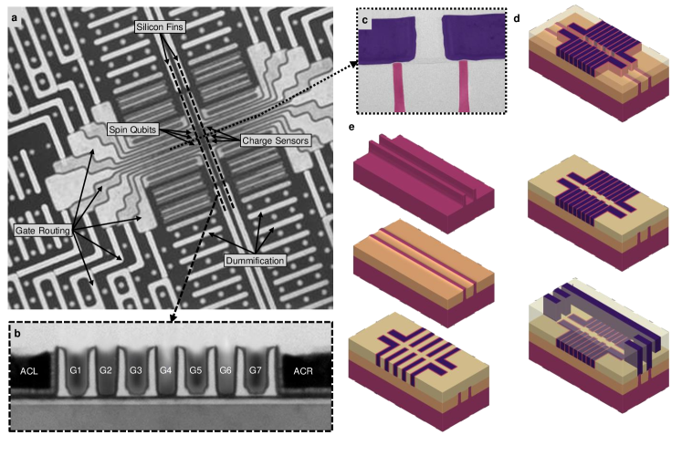
As in current complementary metal-oxide-semiconductor (CMOS) transistors, the active region of these quantum dot devices consists of a fin etched out of the silicon substrate auth2017 . Nested top-gates with a pitch of nm, separated from the fin by a composite SiO2/high-k dielectric, are used to form and manipulate quantum dots. Figure 1a shows a high-angle annular dark-field scanning transmission electron microscopy (HAADF-STEM) image of the active device area. A cross-section transmission electron microscopy (TEM) image along a fin with quantum dot gates is shown in Fig. 1b. N-type ion implants on both ends of the fin, well separated from the active region, serve as Ohmic contacts to the fins. We pattern two such linear quantum dot arrays, separated by 100 nm (see Fig. 1c for a TEM image across both fins). In our experiments, we use a quantum dot in one array as a charge sensor for the quantum dots and qubits in the other array. A 3D device schematic is shown in Fig. 1d.
The process flow starts from a conventional transistor flow but is adapted to fabricate two sets of gates in successive steps using a combination of 300 mm optical lithography, thin film deposition, plasma etch, and chemical mechanical polish processes. The main steps are illustrated in Fig. 1e. First, the fins are defined in a Si substrate. The area between the fins is filled in with a shallow trench isolation dielectric material and polished. The first gate layer (with even numbers) is defined using an industry standard replacement metal gate process natarajan_32nm_2008 ; auth_22nm_2012 ; mistry_logic_2007 and the second gate layer (with odd numbers) is then formed adjacent to the first gate layer. Finally, a contact layer is patterned to enable routing to bond pads, as well as ohmic and gate contacts. In the devices intended for coherent experiments (discussed in Fig. 4), a metal wire that shunts a coplanar stripline (connected to an on-chip coplanar waveguide) is placed parallel to the fins in the contact layer (Extended Data Fig. 2). The samples used only for quantum dot formation are fabricated on natural silicon substrates, whereas the samples used for qubit readout and manipulation are fabricated on an isotopically enriched 28Si epilayer with a residual 29Si concentration of 800 ppm sabbagh_quantum_2019 . This reduces the hyperfine interaction of the qubits with nuclear spins in the host material and thus increases the qubit coherence zwanenburg_silicon_2013 .
A single 300 mm wafer contains more than quantum dot arrays of various lengths, with up to 55 gates per fin. The impact of the industrial fabrication is immediately clear when we compare the TEM image of a 7-gate device in Fig. 1b to a TEM image of an academic Si-MOS device (see Extended Data Fig. 1); the gate uniformity is remarkable and there are no traces of residual metallic pieces. This uniformity is reflected in e.g. the threshold voltage of individual gates within quantum dot arrays, as well as across quantum dot arrays throughout the wafer, measured at room temperature (see Extended Data Fig. 3).
All quantum dot and qubit measurements are carried out in a dilution refrigerator, operated at base temperature. The measurements have been performed on a plethora of different devices from different process flow generations, measured in three different dilution refrigerators in different laboratories. Samples of the same generation taken from anywhere across the wafer show very reproducible quantum dot behaviour.
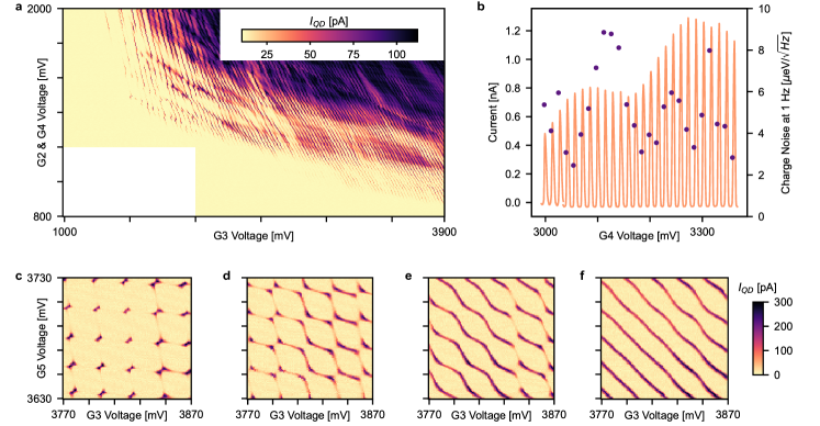
We form quantum dots by tuning the gates individually to define a suitable potential landscape (dots can be controllably formed below any of the inner 5 gates). Figure 2a shows a typical result, where we measure the current through a QD while sweeping three gate voltages, one of which mostly controls the electrochemical potential (labeled G3 in Fig. 1b) of the quantum dot and the others (G2 and G4) mostly control the tunnel barriers. Starting at a G3 gate voltage of 3.9 V, we count more than 80 lines, known as Coulomb peaks, separating regions with a stable number of electrons on the QD. This number is changed by exactly one when passing a Coulomb peak. While the Coulomb peaks are parallel and evenly spaced at a high G3 voltage ( 3 V), they become irregular and also further separated towards the few-electron regime (around 1.5 V on G3). Such irregular behaviour is characteristic of Si-MOS devices, due to their close proximity to the dielectric interface veldhorst_addressable_2014 ; maurand_cmos_2016 ; petit_spin_2018 ; yang_operation_2020 ; veldhorst_two-qubit_2015 ; huang_fidelity_2019 ; harvey-collard_spin-orbit_2019 ; li_flexible_2020 .
Analysing these first-generation dots through so-called Coulomb diamonds hanson_spins_2007 , gives an average charging energy of meV (all error bars are 1 from the mean) per dot in the multi-electron regime (see Extended Data Fig. 4). This indicates the dot diameter to be on the order of nm, which is about the width of a single gate. Next, we measure charge noise in the multi-electron regime, by measuring the current fluctuations at a fixed gate voltage, on the flank of a Coulomb peak. The power spectral density shows a 1/ slope that is characteristic of charge noise in solid-state devices paladino_1_2014 . The charge noise amplitude is in the range of eV/ at Hz, with some variation between Coulomb peaks (Fig. 2b). These are common charge noise values in Si-MOS QD samples petit_spin_2018 .
Figure 2c shows the transport through a double QD as a function of the gate voltages that (mostly) control the electrochemical potential of each dot, G3 and G5. Characteristic points of conductance are measured, so-called triple points. At these points, the electrochemical potentials of the reservoirs are aligned with the electrochemical potentials of the left and the right dot, such that electrons can tunnel sequentially through the two dots van_der_wiel_electron_2002 . Increasing the voltage applied to the intermediate gate G4 is expected to lower the tunnel barrier between the dots, eventually reaching the point where one large dot is formed. This behaviour is seen in Figs. 2c-f, as the gradual transition from triple points to single, parallel and evenly spaced Coulomb peaks. This shows the tunability of the interdot tunnel coupling in this double dot, which is advantageous for two-qubit control in such a system zajac_resonantly_2018 ; yang_operation_2020 ; takeda_quantum_nodate ; xue_cmos-based_2020 .
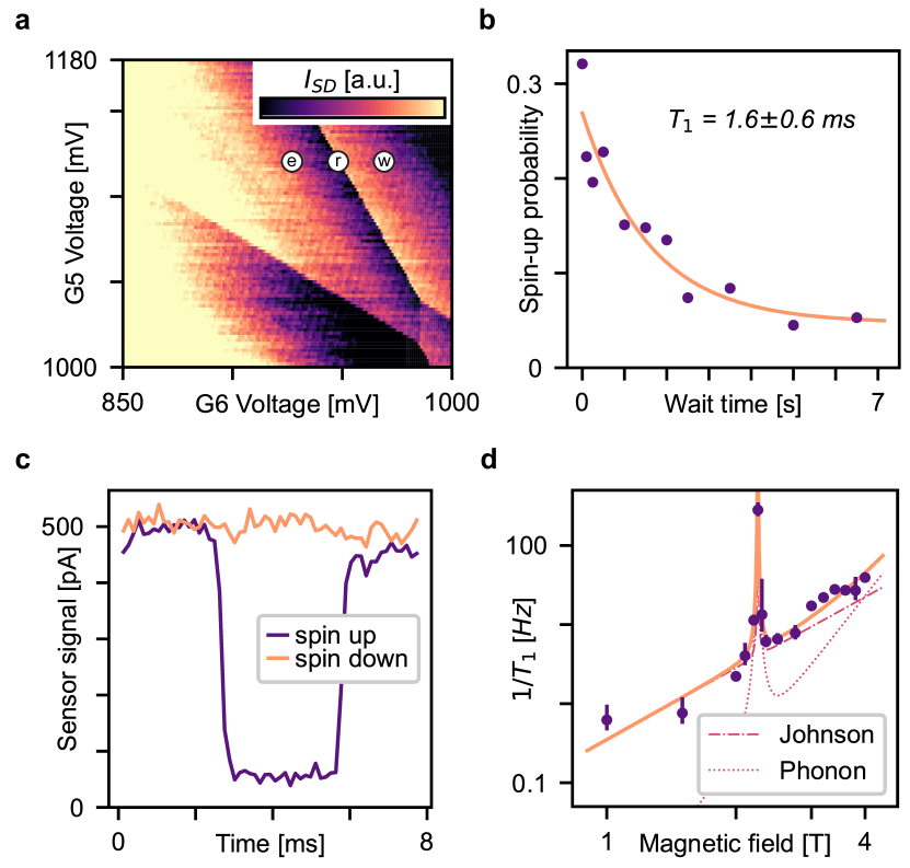
In a next step, we use a QD in one fin as a charge sensor for the charge occupation of the QDs in the other fin. This allows us to unambiguously map the charge states of the qubit dots down to the last electron hanson_spins_2007 . A characteristic charge stability diagram showing the last electron transition is shown in Fig. 3a. The current through the sensor is measured as a function of the voltage on two gates controlling the qubit dot. In the few-electron regime, we can usually distinguish lines with several different slopes, indicating the formation of additional, spurious dots next to the intended dot. However, we consistently are able to find a clean region in the charge stability diagram with an isolated addition line corresponding to the last electron. Several iterations of geometry and material changes improved the charge sensing by orders of magnitude, resulting in a sensing step of about pA for a source-drain voltage of 500 V. This allows single-shot readout of the spin of a single electron by means of spin-dependent tunneling and real-time charge detection (Fig. 3c) elzerman_single-shot_2004 .
In order to define a qubit via the electron spin states, we apply a magnetic field in the -direction, parallel to the fins, separating the spin-up and spin-down levels in energy. We apply a three-stage pulse to gate G6 to measure the spin relaxation time, elzerman_single-shot_2004 . We find exceeding s at a magnetic field of 1 Tesla (Fig. 3b). This long is comparable to those reported previously for silicon quantum dots petit_spin_2018 ; yang_operation_2020 and indicates that the more complicated processing conditions of the 300 mm-scale fabrication do not degrade the spin relaxation time. Upon measuring as a function of magnetic field, we find a striking, non-monotonic dependence, which is well described in the literature and the result of the valley structure in the conduction band of silicon. Following yang_spin-valley_2013 ; petit_spin_2018 , we fit the magnetic field dependence of the spin relaxation rate () with a model including the effect of Johnson noise and phonons inducing spin transitions mediated by spin-orbit coupling, and taking into account the lowest four valley states (Fig. 3d). The peak in the relaxation rate around T corresponds to the situation where the Zeeman energy equals the valley splitting energy, from which we extract a valley splitting of eV, well above the thermal energy and qubit splitting in this system.
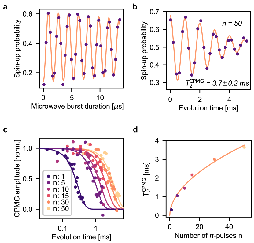
To coherently control the spin states, we apply an ac current to the stripline in order to generate an oscillating magnetic field at the QD koppens_driven_2006 . Electron spin resonance occurs when the driving frequency matches the spin Larmor frequency of GHz, which is set by the static magnetic field at the dot. By pulsing the spin-down level below the Fermi reservoir, we load the QD with a spin-down electron. We then pulse deep in the Coulomb blockade regime to manipulate the spin with microwave bursts. Finally, we pulse to the readout point and perform spin-dependent tunneling readout. The spin-up probability as a function of microwave burst duration shows clear Rabi oscillations, (Fig. 4a). We have studied Rabi oscillations in three devices; the main figures show data for qubit 1 (Q1) and the Extended figures (11, 12 and 13) show data for qubit 2 (Q2), formed on the same device, and qubit 3. As expected, the Rabi frequency is linear in the driving amplitude, reaching up to about kHz for Q2.
The spin dephasing time is measured through a Ramsey interference measurement (see Extended Data Fig. 8). Fitting this Ramsey pattern with a Gaussian-damped oscillation, yields a decay time of when averaging data over 100 s (the error bar here refers to the statistical variation between 41 post-selected repetitions of 100 s segments). As we repeat such Ramsey measurements, we observe slow jumps in the qubit frequency. Averaging the free induction decay over 2 hours and 40 minutes still gives a of , see Methods section for more details.
To analyse the single-qubit gate fidelity, we employ randomised benchmarking knill_randomized_2008 (Extended Fig. 10). A number, , of random Clifford gates is applied to the qubit, followed by a gate that ideally returns the spin to either the spin-up or spin-down state. In reality, the probability to reach the target state decays with due to imperfections. The standard analysis gives a single-qubit gate fidelity of for Q1 and for Q2. With the Rabi decay being dominated by low-frequency noise, the present combination of and Rabi frequency should allow an even higher fidelity veldhorst_two-qubit_2015 ; petit_universal_2020 ; yang_operation_2020 . We suspect the single-qubit gate fidelity to be limited by improper calibration. Nonetheless, the fidelity is already around the fault-tolerant threshold for the surface code fowler_surface_2012 .
Finally, we study the limits of spin coherence by performing dynamical decoupling by means of Carr-Purcell-Meiboom-Gill (CPMG) sequences (see Fig. 4b for the coherence decay using 50 pulses). These sequences eliminate the effect from quasi-static noise sources. Figure 4c shows the normalised amplitude of the CPMG decay as a function of evolution time for different numbers of -pulses, . By fitting these curves we extract . We use a Gaussian decay envelope which yields distinctly better agreement than an exponential decay. The times are plotted as a function of in Fig. 4d. We obtain a of over ms for CPMG pulses, more than 100 times larger than , with room for further increases through additional decoupling pulses. The CPMG data for Q1 is consistent with charge noise as the limiting mechanism (see Methods). For Q2, an additional noise mechanism is likely present. Again, all the decay timescales are comparable to the results reported earlier for 28Si-MOS devices veldhorst_addressable_2014 ; veldhorst_two-qubit_2015 ; petit_spin_2018 ; yang_operation_2020 ; harvey-collard_spin-orbit_2019 ; maurand_cmos_2016 .
In summary, despite the industrial processing conditions used to fabricate the qubit samples, key performance indicators such as charge noise, the charge sensing signal, , and , are already state-of-the-art. The formation of easily tunable double dots bodes well for the implementation of two-qubit gates in this system. Several further improvements are possible. First, the ESR stripline can be redesigned to lower resistance and dissipation by increasing the trace width up to the short and using lower resistivity materials. Furthermore, bringing the quantum dots on the inside of the stripline koppens_driven_2006 will increase the ratio of magnetic field and (unwanted) electric fields and heating. Finally, spurious dots in the few electron regime and two-level systems can be removed by reducing the presence of material charge defects nicollian82 ; schulz83 . While growth conditions for high-quality Si/dielectric interfaces have been identified, performance-limiting defects can be formed through downstream processing. Further work is ongoing to optimise the process flow and recipes (temperature budget, plasma conditions, chemical exposure, and annealing conditions) to reduce defects at the end of line.
These fabrication methods can be adapted to allow for 2D quantum dot arrays as well. Moreover, these processing steps are by default integratable with any other CMOS technology, which opens up the potential to integrate classical circuits next to the qubit chip. Eventually, industrial processing has the potential to achieve the very high quantum dot uniformity that would enable cross-bar addressing schemes li_crossbar_2018 . The compatibility of silicon spin qubits with fully-industrial processing demonstrated here, highlights their potential for scaling and for realising a fault-tolerant full-stack quantum computer.
References
- (1) Campbell, E. T., Terhal, B. M. & Vuillot, C. Roads towards fault-tolerant universal quantum computation. Nature 549, 172–179 (2017).
- (2) Wecker, D., Bauer, B., Clark, B. K., Hastings, M. B. & Troyer, M. Gate-count estimates for performing quantum chemistry on small quantum computers. Phys. Rev. A 90, 022305 (2014).
- (3) Veldhorst, M. et al. An addressable quantum dot qubit with fault-tolerant control-fidelity. Nat. Nanotechnol. 9, 981–985 (2014).
- (4) Maurand, R. et al. A CMOS silicon spin qubit. Nat. Commun. 7, 13575 (2016).
- (5) Petit, L. et al. Spin lifetime and charge noise in hot silicon quantum dot qubits. Phys. Rev. Lett. 121, 076801 (2018).
- (6) Yang, C. H. et al. Operation of a silicon quantum processor unit cell above one kelvin. Nature 580, 350–354 (2020).
- (7) Harvey-Collard, P. et al. Spin-orbit interactions for singlet-triplet qubits in silicon. Phys. Rev. Lett. 122, 217702 (2019).
- (8) Xue, X. et al. Benchmarking gate fidelities in a Si/SiGe two-qubit device. Phys. Rev. X 9, 021011 (2019).
- (9) Yoneda, J. et al. A quantum-dot spin qubit with coherence limited by charge noise and fidelity higher than 99.9%. Nat. Nanotechnol. 13, 102–106 (2018).
- (10) Watson, T. F. et al. A programmable two-qubit quantum processor in silicon. Nature 555, 633–637 (2018).
- (11) Zajac, D. M. et al. Resonantly driven CNOT gate for electron spins. Science 359, 439–442 (2018).
- (12) Andrews, R. W. Quantifying error and leakage in an encoded Si/SiGe triple-dot qubit. Nat. Nanotechnol. 14, 5 (2019).
- (13) Wu, X. et al. Two-axis control of a singlet-triplet qubit with an integrated micromagnet. Proc. Natl. Acad. Sci. USA 111, 11938–11942 (2014).
- (14) Li, R. et al. A flexible 300 mm integrated Si MOS platform for electron- and hole-spin qubits exploration. In International Electron Devices Meeting 38.3.1–38.3.4 (IEEE, 2020).
- (15) Pillarisetty, R. et al. Qubit device integration using advanced semiconductor manufacturing process technology. In International Electron Devices Meeting 133–136 (IEEE, 2018).
- (16) Feynman, R. P. Simulating physics with computers. Int. J. Theor. Phys. 21, 467–488 (1982).
- (17) Bravyi, S. B. & Kitaev, A. Y. Quantum codes on a lattice with boundary. Preprint at arXiv:quant-ph/9811052 (1998).
- (18) Fowler, A. G., Mariantoni, M., Martinis, J. M. & Cleland, A. N. Surface codes: towards practical large-scale quantum computation. Phys. Rev. A 86, 032324 (2012).
- (19) Loss, D. & DiVincenzo, D. P. Quantum computation with quantum dots. Phys. Rev. A 57, 120–126 (1998).
- (20) Zwanenburg, F. A. et al. Silicon quantum electronics. Rev. Mod. Phys. 85, 961–1019 (2013).
- (21) Vandersypen, L. M. K. & Eriksson, M. A. Quantum computing with semiconductor spins. Physics Today 72, 38–45 (2019).
- (22) Yang, C. H. et al. Silicon qubit fidelities approaching incoherent noise limits via pulse engineering. Nat. Electron. 2, 151–158 (2019).
- (23) Veldhorst, M. et al. A two-qubit logic gate in silicon. Nature 526, 410–414 (2015).
- (24) Huang, W. et al. Fidelity benchmarks for two-qubit gates in silicon. Nature 569, 532–536 (2019).
- (25) Hendrickx, N., Franke, D., Sammak, A., Scappucci, G. & Veldhorst, M. Fast two-qubit logic with holes in germanium. Nature 577, 487–491 (2020).
- (26) Qiao, H. et al. Conditional teleportation of quantum-dot spin states. Nat. Commun. 11, 3022 (2020).
- (27) Takeda, K., Noiri, A., Nakajima, T., Yoneda, J. & Kobayashi, T. Quantum tomography of an entangled three-spin state in silicon. Preprint at arXiv:2010.10316 21.
- (28) Hendrickx, N. W. et al. A four-qubit germanium quantum processor. Preprint at arXiv:2009.04268 (2020).
- (29) Petit, L. et al. Universal quantum logic in hot silicon qubits. Nature 580, 355–359 (2020).
- (30) Vandersypen, L. M. K. et al. Interfacing spin qubits in quantum dots and donors—hot, dense, and coherent. npj Quant. Inf. 3, 34 (2017).
- (31) Veldhorst, M., Eenink, H. G. J., Yang, C. H. & Dzurak, A. S. Silicon CMOS architecture for a spin-based quantum computer. Nat. Commun. 8, 1766 (2017).
- (32) Li, R. et al. A crossbar network for silicon quantum dot qubits. Sci. Adv. 4 (2018).
- (33) Pauka, S. J. et al. A cryogenic interface for controlling many qubits. Preprint at arXiv:1912.01299 (2019).
- (34) Xue, X. et al. CMOS-based cryogenic control of silicon quantum circuits. Preprint at arXiv:2009.14185 (2020).
- (35) Auth, C. et al. A 10nm high performance and low-power CMOS technology featuring 3rd generation FinFET transistors, self-aligned quad patterning, contact over active gate and cobalt local interconnects. In International Electron Devices Meeting 29.1.1–29.1.4 (IEEE, 2017).
- (36) Van Zant, P. Microchip Fabrication: A Practical Guide to Semiconductor Processing, 6th Edition (McGraw-Hill, New York, 2014).
- (37) Averin, D. V. & Likharev, K. K. Coulomb blockade of single-electron tunnelling, and coherent oscillations in small tunnel junctions. J. Low Temp. Phys. 62, 345–373 (1986).
- (38) van der Wiel, W. G. et al. Electron transport through double quantum dots. Rev. Mod. Phys. 75, 1–22 (2002).
- (39) Hanson, R., Kouwenhoven, L. P., Petta, J. R., Tarucha, S. & Vandersypen, L. M. K. Spins in few-electron quantum dots. Rev. Mod. Phys. 79, 1217–1265 (2007).
- (40) Chanrion, E. et al. Charge detection in an array of CMOS quantum dots. Phys. Rev. Applied 14, 024066 (2020).
- (41) Natarajan, S. et al. A 32nm logic technology featuring 2nd-generation high-k + metal-gate transistors, enhanced channel strain and 0.171m2 sram cell size in a 291mb array. In International Electron Devices Meeting 1–3 (IEEE, 2008).
- (42) Auth, C. et al. A 22nm high performance and low-power CMOS technology featuring fully-depleted tri-gate transistors, self-aligned contacts and high density MIM capacitors. In Symposium on VLSI Technology (VLSIT) 131–132 (VLSIT, 2012).
- (43) Mistry, K. et al. A 45nm logic technology with high-k+metal gate transistors, strained silicon, 9 Cu interconnect layers, 193nm dry patterning, and 100% Pb-free packaging. In International Electron Devices Meeting 247–250 (IEEE, 2007).
- (44) Sabbagh, D. et al. Quantum transport properties of industrial 28Si/28SiO2. Phys. Rev. Applied 12, 014013 (2019).
- (45) Paladino, E., Galperin, Y., Falci, G. & Altshuler, B. 1/f noise: implications for solid-state quantum information. Rev. Mod. Phys. 86, 361–418 (2014).
- (46) Elzerman, J. M. et al. Single-shot read-out of an individual electron spin in a quantum dot. Nature 430, 431–435 (2004).
- (47) Yang, C. H. et al. Spin-valley lifetimes in a silicon quantum dot with tunable valley splitting. Nat. Commun. 4, 2069 (2013).
- (48) Koppens, F. H. L. et al. Driven coherent oscillations of a single electron spin in a quantum dot. Nature 442, 766–771 (2006).
- (49) Knill, E. et al. Randomized benchmarking of quantum gates. Phys. Rev. A 77, 012307 (2008).
- (50) Nicollian, E. & Brews, J. MOS (Metal Oxide Semiconductor) Physics and Technology (John Wiley & sons, New York, 1982).
- (51) Schulz, M. Interface states at the SiO2-Si interface. Surface Science 132, 422–455 (1983).
- (52) Bylander, J. et al. Noise spectroscopy through dynamical decoupling with a superconducting flux qubit. Nat. Phys. 7, 565–570 (2011).
- (53) Cywinski, L., Lutchyn, R. M., Nave, C. P. & Das Sarma, S. How to enhance dephasing time in superconducting qubits. Phys. Rev. B 77, 11 (2008).
Methods
Setup and instrumentation
The measurements were performed on two different setups on different continents, setup 1 (S1, Delft) and setup 2 (S2, Hillsboro). The samples were cooled down in a dilution refrigerator, operated at the base temperature of around mK (S1: Oxford Triton dry dilution refrigerator, S2: Bluefors XLD dry dilution refrigerator). DC voltages were applied via Delft in-house built, battery-powered voltage sources (S1 and S2). The printed circuit board onto which the sample was mounted contained bias tees with a cut-off frequency of 3 Hz to allow for the application of gate voltage pulses (S1 and S2). The pulses were generated by an arbitrary waveform generator (AWG, S1: Tektronix AWG5014, S2: Zurich Instruments HDAWG). The baseband current through the sensing dot was converted to a voltage by means of a home-built amplifier, filtered through a room-temperature low-pass filter (S1: 3 kHz, S2: 1.5 kHz) and sampled by a digitiser (S1: M4i spectrum, S2: Zurich Instruments MFLI). Microwave bursts for driving ESR were generated by a vector source with an internal IQ mixer (S1 and S2: Keysight PSG8267D), with the I and Q channels controlled by two output channels of the AWG.
Charge noise measurements
Each charge noise data point in Fig. 2c is obtained by recording a 140 second time trace (at 28 Hz sampling rate) of the current through the QD with the plunger gate voltage fixed at the steepest point of the Coulomb peak flank. To convert the current signal to energy, we proceed as follows. First, we convert the current to gate voltage by multiplying the data by the slope of the Coulomb peak at the operating point. Then, we multiply with the lever arm to convert from plunger gate voltage to energy. To obtain the power spectral density (PSD), we divide the data in 10 equally long segments, take the single-sided fast Fourier transform (FFT) of the segments and average these. Fitting the PSD to we extract the energy fluctuations at 1 Hz () for each Coulomb peak. We extract a mean value of .
Spin readout
In order to read out the spin eigenstate we use energy-selective tunneling to the electron reservoir elzerman_single-shot_2004 . The spin levels are aligned with respect to the Fermi reservoir, such that a spin-up electron can tunnel out of the QD, while for a spin-down electron it is energetically forbidden to leave the QD. Thus, depending on the spin state, the charge occupation in the QD will change. To monitor the charge state, we apply a fixed voltage bias across the sensing dot and measure the baseband current signal through the sensing dot, filtered with a low-pass filter and sampled via the digitiser. In post-analysis we threshold the sensing dot signal and accordingly assign a spin-up or spin-down to every single shot experiment. After readout, we empty the QD to repeat the sequence. As is commonly seen in spin-dependent tunneling, the readout errors are not symmetric, which is reflected in the range of the oscillations in Figs. 4a,b.
Qubit operations
When addressing the qubit, we phenomenologically observe that the qubit resonance frequency shifts depending on the burst duration. The precise origin of this resonance shift is so-far unclear, but appears to be caused by heating. Similar observations have been made in recent spin qubit experiments watson_programmable_2018 ; yoneda_quantum-dot_2018 ; xue_cmos-based_2020 that used electric-dipole spin resonance via micromagnets as the driving mechanism. To ensure a reproducible qubit frequency in the experiments, we apply an off-resonant microwave burst prior to the intended manipulation phase to saturate this frequency shift. We further investigate this frequency shift in Extended Data Figs. 6 and 7.
Ramsey oscillation
We observe that the qubit resonance frequency in the devices exhibits jumps of several 100 s of kHz on a timescale of 5-10 minutes. To extract meaningful results, we monitor this frequency shift throughout the experiments and accordingly discard certain data traces, such that we only take into account data acquired with the qubit in a narrow frequency window.
To illustrate the frequency shift, we show the FFT of 100 repetitions of a Ramsey interference measurement of qubit 1 (measurement time 2 hours 40 min) in Extended Data Fig. 8a, which tracks the qubit frequency over time. In order to estimate the of qubit 1, we fit each of the 100 repetitions of the Ramsey measurement (measurement time per repetition 100 s) and extract a value. Evidently, some of the data quality is rather poor due to the previously described frequency jumps in which case the extracted value is meaningless. We calculate the mean square error of each fit and disregard all the measurements with a high error. The average of the 41 remaining traces is s (Extended Data Fig. 8b). Averaging the data traces of all 41 traces and then fitting a decay curve yields a dephasing time of s (Extended Data Fig. 8c); averaging the data of all 100 traces still gives a dephasing time of s (Extended Data Fig. 8d).
CPMG coherence measurements and power spectral density
To ensure robust fitting, the CPMG sequences are applied with artificial detuning. We fit the resulting curves with a Gaussian damped cosine function: . If, instead of using a Gaussian decay, we leave the exponent of the decay open as a fitting parameter, we obtain values for the exponent between 2.3 and 2.6, but the use of the additional parameter results in less robust fits. The offset is included to compensate for the loss of readout visibility for long microwave burst duration. We attribute this to heating generated while driving the spin rotations. The measurement is divided into segments, each consisting of 200 single shots. Each segment includes a simple calibration part, based on which we post-select repetitions for which the spin-up probability after applying a -pulse is above 25 percent. In this way, we can exclude repetitions where the qubit resonance frequency has shifted drastically. The remaining repetitions are averaged to obtain the characteristic decay curves for each choice of , one of which is shown in Fig. 4b.
From fitting the decay curves, we extract the times as a function of , shown in Fig. 4d. To extract the CPMG amplitude as a function of evolution time from the data, we demodulate the measured values with the parameters extracted from the fit, according to , with the measured data. Due to experimental noise, points where the denominator is small, do not yield meaningful results. Hence, we exclude data points for which the absolute value of the expected denominator is smaller than 0.4. The extracted CPMG amplitudes are plotted in Fig. 4c.
In a commonly used simplified framework bylander_noise_2011 ; cywinski_how_nodate , we can relate the data of Fig. 4d to a noise power spectral density of the form . Specifically, fitting the data to gives . Alternatively, we can estimate by fitting the noise power spectral density extracted from the individual data points in the CPMG decays cywinski_how_nodate in Extended Data Fig. 9(a). This analysis gives . Either way, the extracted power spectral density is close to the dependence that is characteristic of charge noise. Charge noise can affect spin coherence since the spin resonance frequency is sensitive to the gate voltage, as also reported before for Si-MOS based spin qubits veldhorst_addressable_2014 . We next estimate how large charge noise would need to be in order to dominate spin decoherence. To do so, we extrapolate the extracted spectral density in the range between and Hz to an amplitude at Hz, which after conversion to units of charge noise gives eV/. With the caveat that this extrapolation is not very precise, we note that this value is only slightly larger than the charge noise amplitude in the multi-electron regime of eV/. Considering that charge noise values are typically higher in the few-electron regime, this suggests that coherence of Q1 may be limited by charge noise cywinski_how_nodate . For Q2, which is another qubit in the same sample, the same procedure gives an extrapolated noise at 1 Hz that is an order of magnitude larger. Possibly a two-level fluctuator is active in the vicinity of this qubit in the regime where the qubit data was taken.
Acknowledgements
We thank Luca Petit and Sander de Snoo for software support and Raymond Schouten, Raymond Vermeulen, Marijn Tiggelman, Jason Mensingh, Olaf Benningshof and Matt Sarsby for technical support. Moreover, we thank all people from the QuTech spin qubit group and from the Intel Components research group for discussions. We acknowledge financial support from Intel Corporation and the QuantERA ERA-NET Cofund in Quantum Technologies implemented within the European Union’s Horizon 2020 Program.
Author contributions
A.M.J.Z., T.K., T.F.W., L.L. and F.L. performed the quantum dot and qubit measurements. J.B., D.C.S., J.P.D., G.D., R.K., D.J.M., R.P., N.S., G.S., M.V., L.M.K.V. and J.C. designed the devices. S.A.B., H.C.G., E.M.H. and B.K.M. fabricated the devices. P.A., J.M.B., R.C., T.K., L.L., F.L., D.M., S.N., R.P., T.F.W., O.K.Z., G.Z. and A.M.J.Z. characterised the test structures and devices. M.L. characterised the Si-MOS stacks. S.V.A. contributed to the preparation of the experiments. A.M.J.Z., T.K., T.F.W., L.L. and F.L. analysed the data. J.R., L.M.K.V. and J.S.C. conceived and supervised the project. A.M.J.Z., T.K. and L.M.K.V. wrote the manuscript with input from all authors.
Additional information
Data availability
Datasets and analysis scripts supporting the conclusions of this paper are available at https://doi.org/10.5281/zenodo.4478855.
Competing interests
The authors declare no competing interests.