Inverse Design of Whispering-gallery Nanolasers with Tailored Beam Shape and Polarization
Abstract
Control over the shape and polarization of the beam emitted by a laser source is important in applications such as optical communications, optical manipulation and high-resolution optical imaging. In this paper, we present the inverse design of monolithic whispering-gallery nanolasers which emit along their axial direction with a tailored laser beam shape and polarization. We design and experimentally verify three types of sub-micron cavities, each one emitting into a different laser radiation mode: an azimuthally polarized doughnut beam, a radially polarized doughnut beam and a linearly polarized gaussian-like beam. The measured output laser beams yield a field overlap with respect to the target mode of 92%, 96% and 85% for the azimuthal, radial and linearly polarized cases, respectively, thereby demonstrating the generality of the method in the design of ultra-compact lasers with tailored beams.
keywords:
inverse design, topology optimization, nanolasers, whispering-gallery mode, far-field, beam tailoringUniversity of Exeter] College of Engineering, Mathematics and Physical Sciences, University of Exeter, EX4 4QF, Exeter, United Kingdom University of Sheffield] EPSRC National Epitaxy Facility, University of Sheffield, S1 3JD, Sheffield, United Kingdom University of Exeter] College of Engineering, Mathematics and Physical Sciences, University of Exeter, EX4 4QF, Exeter, United Kingdom \abbreviationsWGM, QW, TO, FoM, AP, RP, LP {tocentry}
![[Uncaptioned image]](/html/2207.09836/assets/threeNanolasers.png)
1 Introduction
Spatial control over the shape and polarization of the beam emitted by a laser source is becoming increasingly relevant for applications such as polarization multiplexing in optical communications 1, 2, stiffer optical trapping 3 and high-resolution optical imaging 4. This tailoring of the beam is conventionally done with optics external to the source, but recently there has been interest in structuring light at the source5. This is specially relevant to meet the growing demand for higher density photonic integration and for further miniaturization of laser sources6, 7. However, on-chip generation of tailored laser beams has not yet been realized for cavities under the sub-micron footprint.
One of the most compact types of integrated cavities are the optical whispering-gallery mode microdisc laser, which exhibit large quality factors and low mode volumes, thereby enhancing the light-matter interaction resulting in low lasing threshold. These properties make them excellent systems for applications such as biochemical sensing 8, 9, cell barcoding and tracking10, 11 and optical communications 12. However, due to their circular geometry, the laser light is radiated in-plane and isotropically 11, 13. This limits their range of use due to the poor collection efficiency in the axial direction and to date there has been little effort to engineer the emission beam shape and/or polarization.
Previous work to achieve vertical emission from WGM lasers has focused on the addition of an angular grating that scatters the light out of the plane. The gratings have been fabricated by metal deposition on top of the microdisc cavity 14, by etching at the inner wall of a microring cavity 15, 16 or at the outer wall of a microdisc cavity 17. In all these examples, the cavities present a lateral footprint larger than 2 m in diameter and polarization control over the radiated beam was only demonstrated for a microring cavity of 120 m diameter 16.
In this work, we present an alternative approach, whereby an inverse design algorithm is applied to optimize a sub-micron scale WGM-cavity design for axial emission, with on-demand laser beam shape and polarization. Inverse design is a powerful tool for discovering novel geometries and for optimizing performance, which is not reliant on the intuition of the user. The inverse design process follows an iterative optimization strategy that allows exploration of the whole design parameter space and has been shown to be effective in a variety of applications, including: maximization of band gaps in photonic crystals 18; wide-angle diffractive optical elements 19; photon extractors for nitrogen-vacancy centers 20, 21; power splitters in integrated photonics 22; coupling of an optical antenna-LED to a single-mode waveguide 23 and on-chip resonators24.
Here, we implement a topology optimization (TO) algorithm 25, 26 for tailoring the laser beam shape and polarization. To show the generality of the method we apply it to the design of three WGM-cavities, each one emitting into a different radiation mode: two spatially varying polarization doughnut beams with azimuthal (AP) and radial (RP) polarization; and a spatially homogeneous linearly polarized (LP) gaussian-like beam. The three different designs are achieved for the same WGM and for a wavelength in the range 650 – 700 nm (chosen to coincide with the QW gain spectral range). The nanocavity designs are fabricated from a GaInP/AlGaInP double quantum well (QW) wafer and their lasing and far-field verified by Fourier microscopy, k-space polarimetry and photoluminescence spectroscopy.
2 Inverse Design Problem
The inverse design of the nanocavity geometry is performed using an adjoint-based topology optimization (TO) method, illustrated schematically in Figure 1. TO is a computational technique for inverse design that can handle extensive design spaces considering the dielectric permittivity at every spatial point as a design variable. The algorithm maximizes the overlap between the mode radiated by the cavity, , and the desired radiation mode, in free space: ; this overlap is the Figure of Merit (FoM) or objective function of our TO problem. This approach gives control over the final output beam shape and polarization by allowing the user to select an appropriate target mode . The adjoint method allows the efficient computation of the optimization gradient, which indicates how to evolve the cavity geometry with only two electromagnetic simulations, known as the forward and adjoint simulations, regardless of the number of degrees of freedom 25, 26, 27, 28, 29. The electromagnetic simulations are computed using a finite-difference time-domain Maxwell’s equation solver (Lumerical).

The iterative optimization procedure is initiated with the geometry shown in Figure 1(b), consisting of an inner disk of diameter 754 nm, surrounded by an external 100 nm wide annulus, both with a fixed thickness of 180 nm. The dielectric permittivity of the inner disc was fixed at , by the QW wafer, and the annulus had an initial random distribution of dielectric permittivity ranging from to , with air being the background medium. The optimization is performed only for the annulus in order to keep the cavity structure as a continuous object, i.e. without holes. This initial disc cavity supports a WGM of order 8 in the azimuthal direction and fundamental order along the radial and axial direction, for the target wavelength of .
The simulation space was parametrized with the density parameter , which is a linear transformation on the dielectric permittivity so that the density values range from 0 to 1, i.e. 30.
| (1) |
The spatial resolution of the parametrization was 10 nm in the three directions , , and .
The steps of the iterative TO process are as follows:
- 1.
-
2.
The forward simulation is run. The source used for exciting the WGM inside the cavity was an electric dipole polarized along the radial direction of the disc and placed close to the disc contour, where an antinode of the WGM would be expected. The electric field throughout the design region, and the electric field throughout the FoM plane (field monitor on Figure 1(a)) are recorded. The FoM plane is placed at a distance of m above the top surface of the cavity. We compute the FoM value with:
(2) -
3.
The adjoint simulation is run. The adjoint source is a mode launched from free space above the cavity with the conjugate of the desired spatial distribution of intensity and polarization: . At the end of the simulation, the electric field throughout the design region is recorded.
The resonant wavelength of the particular WGM of interest shifts at each iteration due to the variation in the dielectric distribution within the design region, and therefore must be tracked. The wavelength at which and are recorded is therefore updated at each iteration according to the maximum of the Purcell enhancement.
-
4.
The gradient of the FoM with respect to the density distribution is calculated 26 as: . This gradient indicates whether the dielectric permittivity of each point within the design region should be increased () or decreased (), in order to maximize .
-
5.
Finally, the density distribution is updated: , where is a hyperparameter that controls the evolution rate, but taking into consideration that the new density value is bounded: . In our simulations we chose to approach to infinitesimal changes in the dielectric permittivity while keeping a large enough value to maintain a reasonable run-time for the optimization.
This process is repeated for 100 iterations to check the stability of the optimized design, but can be stopped as soon as converges to a value. The final designs are obtained by binarizing the density distribution from the last iteration with the threshold being 0.5:
3 Results and Discussion
The TO procedure is used to design cavities that radiate into the three different target output beams: azimuthally polarized doughnut (AP), radially polarized doughnut (RP) and linearly polarized gaussian-like (LP). The resulting optimized designs are shown in Figure 1(a).
The convergence to the optimized design can be seen in the evolution of in Figure 2(a). For the three designs, increases gradually up to a saturation value which is stable within . This saturation indicates the TO algorithm has found a local optimum solution for the optimization problem, given the initial density distribution and constraints such as the design region size and the spatial filtering. for the binarized geometries is plotted with a rhombus of the same color as the respective solid lines. There is a drop in value for AP and RP binarized cavities, whereas there is an increase in value for the LP cavity. Figure 2(a) shows the evolution of evaluated by using the near-field recorded at the field monitor. Even though the algorithm is maximizing the near-field overlap, the far-field overlap increases accordingly. The evolution of computed with a far-field projection is shown in the S.I.
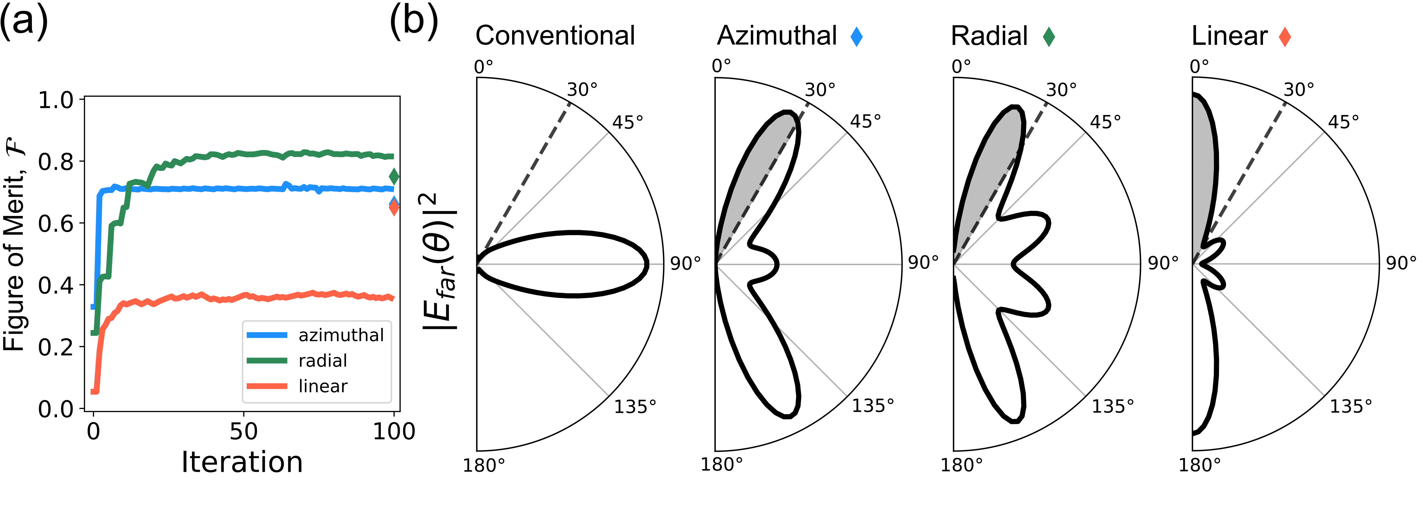
As a consequence of optimizing for a target radiation mode above the cavity, the power radiated out of the plane is increased. This effect can be seen in the radiation diagrams of the optimized cavities plotted in Figure 2(b). These plots show the far-field intensity radiated at each polar angle , upon integration of all azimuthal angles. As discussed in the introduction, the conventional circular cavity radiates most of its power in the plane of the cavity, with a maximum intensity at . In comparison, the optimized designs have maximum intensity at 26.3∘ (AP), 22.3∘ (RP) and 0∘ (LP). Furthermore, the radiated intensity transmitted to a hypothetical objective lens, of numerical aperture 0.5 (maximum acceptance angle 30∘), placed above the cavity is also increased. As summarized in Table 1, the fraction of intensity that is collected by such objective, i.e. the transmitted power , is 21.8% (AP), 20.8% (RP) and 33.7% (LP). Compared to the 2.5% that would be collected from a conventional circular cavity, this corresponds to an enhancement in power collection of 8.7, 8.3 and 13.5, respectively.
| Cavity type | () | Power collection enhancement |
|---|---|---|
| Conventional | 2.5 % | 1 |
| Azimuthal | 22 % | 8.7 |
| Radial | 21 % | 8.3 |
| Linear | 34 % | 13.5 |
3.1 Experimental Verification
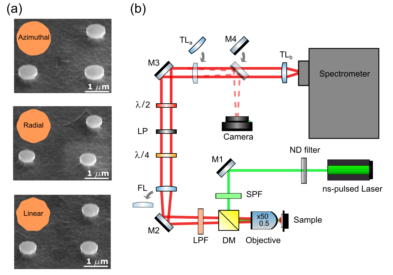
To validate the inverse design approach, we fabricate nanolasers from a GaInP/AlGaInP wafer (simple schematic of the QW in Figure 1(c); full layer structure in S.I.) in the shape of the three different optimized cavity designs (Figure 3(a)) via electron-beam lithography followed by dry and wet etching processes. The nanolasers are characterized using the experimental setup shown schematically in Figure 3(b), and assessed against the following criteria: the overlap between the experimental and desired far-field; the maximum output power; the lasing threshold; and the quality factor. The experimental far-field intensity distributions are obtained by Fourier microscopy and their polarization distribution measured with k-space polarimetry 32. The maximum output power, the lasing threshold and the quality factor are obtained from photoluminescence spectra at different excitation powers. Further detail on the fabrication procedure and optical characterization can be found in the Methods section.
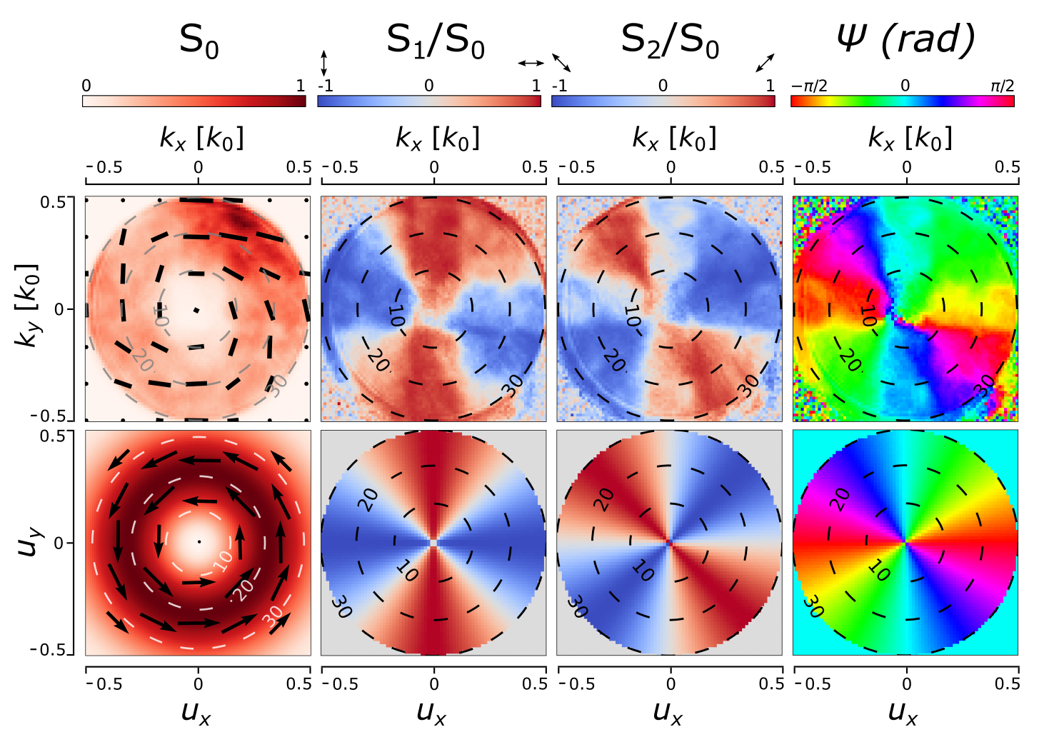
To characterize the nanolasers far-field and polarization, we measure the spatial distribution of the Stokes parameters: is the total intensity; represents the balance between linearly polarized light intensity at 0∘ and 180∘; refers to the balance between linearly polarized light intensity at 45∘ and 135∘; and represents the polarization ellipse orientation 32. With this information it is possible to recreate the polarization (orientation) of the electric field in the far-field , except for its phase. Further details can be found in the S.I.. In the experiment, the Stokes parameters are presented in Fourier space (), where the direction of emission is given by the polar angle obtained as . The Stokes parameters of the target mode are calculated by a far-field projection of the target mode over a hemispherical surface. The target far-field is presented as a top view of this surface with the direction cosines as coordinates (), where the polar angle is obtained as )
Figure 4 presents the experimentally measured spatial distribution of the Stokes parameters for an AP-nanolaser, in comparison to the that of the simulated target AP beam. The experimental shows the expected doughnut shape with an almost uniform intensity distribution and a null-field at as a consequence of its polarization singularity, thus corroborating the vortex nature of the beam33. The vectorial nature of the beam is confirmed by the inhomogeneous polarization distribution shown over . , and are in good agreement with the expected distribution but slightly rotated. This rotation is translated into the beam not being purely azimuthally polarized but actually having a small radial component 34.
A similar comparison is made for RP- and LP-nanolasers, with the experimental and simulated presented in Figure 5 and a full analysis in the S.I. For the RP-nanolaser, shows the expected doughnut shape with a central null-field and radial polarization throughout (Figure 5(a)). For the LP beam, a gaussian-like intensity distribution is obtained; as shown in Figure 5(b). The center of the beam is more intense than the periphery and the majority of the intensity is collected within a cone of . The beam is off the optical axis (Z-axis) by –. Also the null-field or polarization singularity of the RP beam seems to be off axis. This might be due to a small misalignment of the sample stage relative to the optical axis of the objective lens.
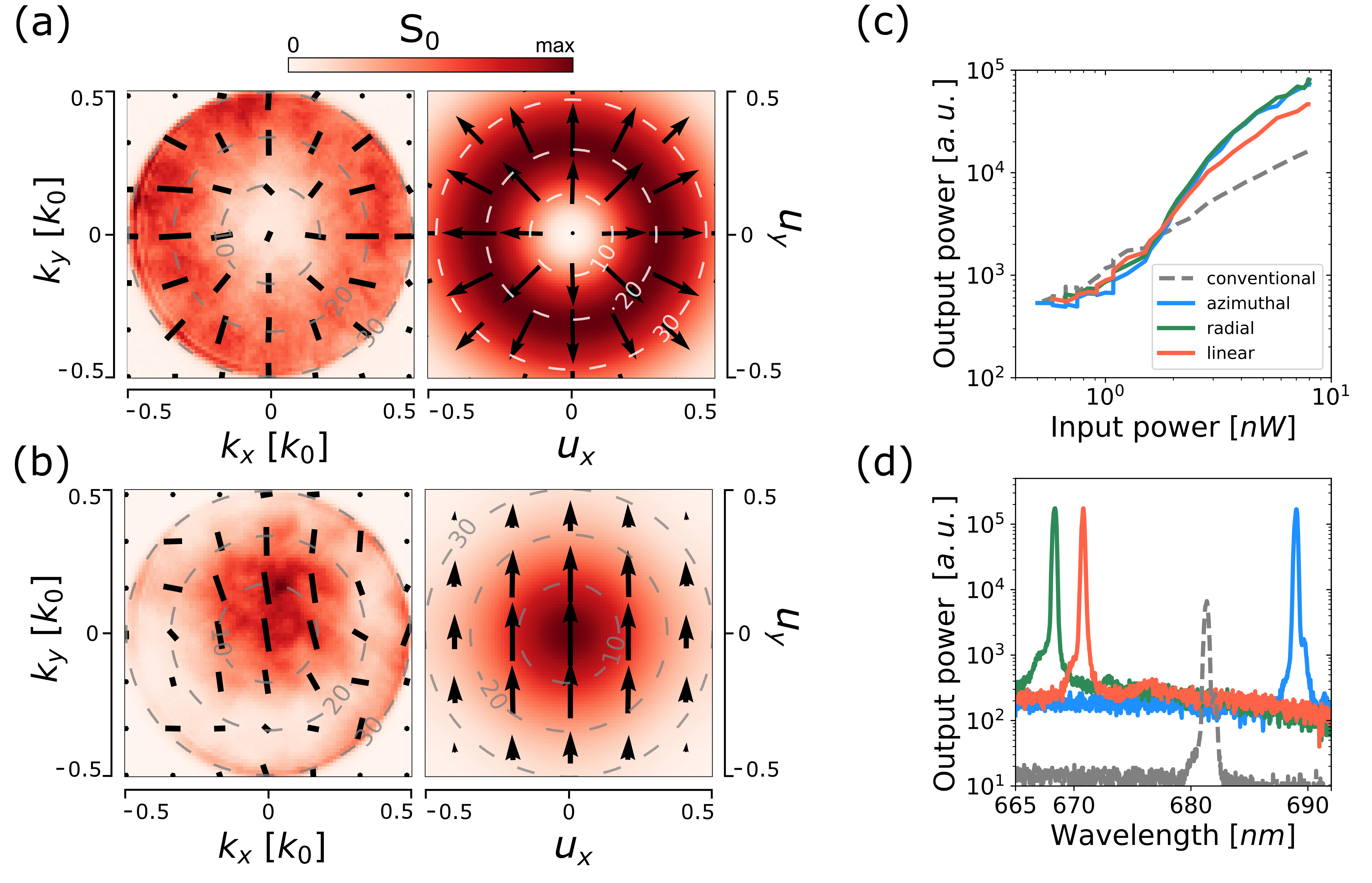
A quantitative assessment of the experimentally obtained far-field modes is calculated by overlapping the experimental far-field with that of the target mode for each nanolaser. The three different far-field modes were described as a superposition of Hermite-Gaussians modes; as indicated in the S.I. This experimental overlap is performed in a similar way as from Equation 2, but not taking into account the phase information: exp. overlap . The overlaps for the AP, RP and LP beams shown in Figure 4 and 5 are 0.92, 0.96 and 0.85, respectively.
To compare the lasing behavior of the different designs, we measured the light-in Vs light-out (L–L) curve for several nanolasers of each type, all of which have an exp. overlap and lasing wavelength between 655 nm and 695 nm (see S.I. for details). To take into account the variation of the lasing mode wavelength and its overlap with the gain spectrum of the QW, we compare the average L–L curve of the ensemble for each type of cavity in Figure 5(c). From fits to these curves, the lasing thresholds were found to be nW (AP), nW (RP), nW (LP), which correspond to pulse energies of 17 pJ (AP), 16.3 pJ (RP), 14.6 pJ (LP), 4.66 pJ (Conv). These values are x3.1 – x3.6 larger than the threshold shown by a conventional cavity of similar size: 0.466 0.032 nW.
The increase in input-output power conversion efficiency of inverse-designed nanolasers when compared to that of the conventional nanolasers was 5.5 (AP), 5.7 (RP), 3.4 (LP) and the increase in maximum output power (at 8 nW input power) was 4.9 (AP), 5.1 (RP) and 2.9 (LP) . This enhancement in the measured output power can be attributed to the enhancement in collection due to the axial emission obtained for the inverse-designed, as shown in Figure 2(b).
The Q-factor of each cavity was obtained from from the photoluminescence spectrum (Figure 5(d)) by obtaining the Full Width Half Maximum, FWHM, of a gaussian fit to the lasing peak. The maximum value of the Q-factors were obtained for input powers near the lasing threshold, with values: 2365 (AP), 2181 (RP), 3250 (LP) and 2239 (Conv).
4 Conclusions
We have shown, using an adjoint-based topology optimization algorithm, that the output beam emitted by a whispering-gallery nanolaser can be tailored in terms of polarization and shape through the design of the contour of its cavity. The generality of this method has been demonstrated through the design of three cavities with different output beam shape and polarization, with the inverse-designed nanolasers exhibiting similar Q-factor and lasing threshold to conventional WGM lasers of comparable size. This control has been achieved within a footprint of less than 1 m2 and opens up the possibility of producing monolithically integrated sub-micron laser sources with on-demand beam characteristics, which has potential in applications such as on-chip label-free biosensing 35, optical manipulation by integrated optical tweezers 36 and free-space optical communications 1.
5 Methods
5.1 Fabrication procedure
The three cavity designs were fabricated on a III-V semiconductor platform with a 180-nm-thick GaInP/AlGaInP double quantum well on a GaAs substrate (EPSRC National Centre for III-V Technologies, Sheffield).
The full layer composition was: 10nm- Ga0.51In0.49P / 58nm- Al0.357Ga0.153In0.49P / 10nm- Al0.255GaIn0.49P / 7nm- Ga0.41In0.59P / 10nm- Al0.255GaIn0.49P / 7nm- Ga0.41In0.59P / 10nm- Al0.255GaIn0.49P / 58nm- Al0.357Ga0.153In0.49P / 10nm- Ga0.51In0.49P.
The semiconductor wafer was cleaved into 1 cm2 chips. Each of the chips were cleaned with sequential ultrasonicated baths in acetone and isopropanol for 10 min each, and then blow-dried with nitrogen. The chips were spin-coated with TI-Prime and then with a 300 nm-thick layer of the negative-tone resist ma-N 2403, and crosslinked on a hot plate at 90 ∘C for 2 min. The pattern was written by electron-beam lithography at 80 kV and beam current 1 nA with a Nanobeam nb4 system. Then the pattern was developed with MF-319 for 20 s and rinsed with deionized-water. The written pattern was transferred from the resist layer to the QW layer by Inductively-Coupled - Reactive Ion Etching (ICP-RIE) with the following conditions: gas-mixture 36 sccm Ar + 4 sccm Cl2, chamber pressure 10 mTorr, RIE power 80 W, ICP power 700 W, sample stage at room temperature and etching time 1 min. The remaining resist was removed by an ultrasonicated bath in hot acetone. Finally, the pedestal under the cavities was formed by a selective wet-underetch with a hydrofluoric acid solution (2.5% w/w in deionized-water) for 1 min.
5.2 Optical characterization
The nanolasers emission was characterized at room temperature via Fourier microscopy and k-space polarimetry. These two techniques allow the imaging of the nanolasers far-field intensity and polarization, respectively. A diagram of the optical setup is shown in Figure 3.
The nanolasers were optically-pumped by a nanosecond-pulsed laser diode at 520 nm (NPL52B, Thorlabs) at a repetition rate of 100 Hz, with a pulse duration of 5 ns. This excitation was coupled through a dichroic beamsplitter (550 nm) into the objective lens (Nikon, x50, numerical aperture 0.5), which focused the excitation light into a 1 m2 diameter spot on the sample. The nanolaser emission was collected by the same objective. A SPF and a LPF with cut-on/-off wavelength 550 nm were placed before and after the DM, respectively, to further spectrally filter the excitation and collection light. The back-focal plane of the objective is directly imaged by a Fourier lens (FL, focal length = 20 cm), which is placed 20 cm away from the back focal plane of the objective, and projected by the infinitely-conjugated tube lens (TL, focal length = 5 cm) onto the fully-open entry slit of the spectrometer (Oxford Instruments - Kymera). The final image is projected onto a CCD camera (Andor iDus 416) by the spectrometer’s diffraction grating at zero-order.
For the polarimetry analysis a quarter-wave plate () and a linear polarizer (LP) were added in the beam path. Different orientations of these two optical components allowed the measurement of the Stokes parameters of the nanolasers emitted far-field. In addition, we needed to introduce a half-wave plate () to rotate the linearly polarized light emerging after the LP to vertical polarization (perpendicular to the optical table) because the spectrometer grating has a larger scattering efficiency for this polarization.
For obtaining the photoluminescence spectrum of a nanolaser the FL is flipped out of the beam path and the spectrometer’s grating (1200 l/mm, blaze 750 nm) is oriented to measure wavelengths within the photoluminescence wavelength range of the QW; from 650 nm to 700 nm. A neutral density (ND) filter was added after the source for varying the excitation power and acquire the L–L curves.
The authors thank S. Wedge for the use of the ICP-RIE at the David Bullet nanofabrication facilities at University of Bath and A. Elliot from the Geography department at University of Exeter for the access to the hydrofluoric acid etching facilities, S. Russo and K.J. Riisnaes for help with preliminary optical characterization experiments. This work was supported by the Engineering and Physical Sciences Research Council (Grant numbers EP/L015331/1 and EP/S001557/1).
The Supporting Information includes further details about: spatial filtering applied in the topology optimization method, Figure of Merit in the far-field, Stokes parameters, polarimetry analysis and experimental overlap calculation, characterization of all measured nanolasers, full layer structure of the quantum well Wafer.
References
- Giovanni Milione, Martin P. J. Lavery, Hao Huang, Yongxiong Ren, Guodong Xie, Thien An Nguyen, Ebrahim Karimi, Lorenzo Marrucci, Daniel A. Nolan, Robert R. Alfano, and Alan E. Willner 2015 Giovanni Milione, Martin P. J. Lavery, Hao Huang, Yongxiong Ren, Guodong Xie, Thien An Nguyen, Ebrahim Karimi, Lorenzo Marrucci, Daniel A. Nolan, Robert R. Alfano, and Alan E. Willner , 4 × 20 Gbit/s mode division multiplexing over free space using vector modes and a q-plate mode (de)multiplexer. Optics Letters 2015, 40, 1980–1983
- D. Ivanovich, C. Zhao, X. Zhang, R. D. Chamberlain, A. Deliwala and V. Gruev 2020 D. Ivanovich, C. Zhao, X. Zhang, R. D. Chamberlain, A. Deliwala and V. Gruev, Chip-to-chip Optical Data Communications using Polarization Division Multiplexing. 2020 IEEE High Performance Extreme Computing Conference 2020, 1–8
- Masaki Michihata, Terutake Hayashi, and Yasuhiro Takaya 2009 Masaki Michihata, Terutake Hayashi, and Yasuhiro Takaya , Measurement of axial and transverse trapping stiffness of optical tweezers in air using a radially polarized beam. Applied Optics 2009, 48, 6143–6151
- Yuichi Kozawa, Daichi Matsunaga, and Shunichi Sato 2018 Yuichi Kozawa, Daichi Matsunaga, and Shunichi Sato, Superresolution imaging via superoscillation focusing of a radially polarized beam. Optica 2018, 5, 86–92
- Andrew Forbes 2019 Andrew Forbes, Structured Light from Lasers. Laser & Photonics Reviews 2019, 13
- Zhou et al. 2015 Zhou, Z.; Yin, B.; Michel, J. On-chip light sources for silicon photonics. Light: Science & Applications 2015, 4
- Wu et al. 2019 Wu, Y.; Hu, X.; Wang, F.; Yang, J.; Lu, C.; Liu, Y.-C.; Yang, H.; Gong, Q. Ultracompact and Unidirectional On-Chip Light Source Based on Epsilon-Near-Zero Materials in an Optical Communication Range. Phys. Rev. Applied 2019, 12, 054021
- Toropov, N., Cabello, G., Serrano, M.P., Gutha, R. R., Rafti, M. and Vollmer, F. 2021 Toropov, N., Cabello, G., Serrano, M.P., Gutha, R. R., Rafti, M. and Vollmer, F., Review of biosensing with whispering-gallery mode lasers. Light Sci Appl 2021, 10
- W. Fang, D. B. Buchholz, R. C. Bailey, J. T. Hupp, R. P. H. Chang, and H. Cao 2004 W. Fang, D. B. Buchholz, R. C. Bailey, J. T. Hupp, R. P. H. Chang, and H. Cao, Detection of chemical species using ultraviolet microdisk lasers. Appl. Phys. Lett. 2004, 85
- Fikouras et al. 2018 Fikouras, A. H.; Schubert, M.; Karl, M.; Kumar, J. D.; Powis, S. J.; Di Falco, A.; Gather, M. C. Non-obstructive intracellular nanolasers. Nature Communications 2018, 9, 4817
- Shui-Jing Tang, Paul H. Dannenberg, Andreas C. Liapis, Nicola Martino, Yue Zhuo, Yun-Feng Xiao and Seok-Hyun Yun 2021 Shui-Jing Tang, Paul H. Dannenberg, Andreas C. Liapis, Nicola Martino, Yue Zhuo, Yun-Feng Xiao and Seok-Hyun Yun, Laser particles with omnidirectional emission for cell tracking. Light Sci Appl 2021, 10
- Zhukov, A.E., Kryzhanovskaya, N.V., Moiseev, E.I., Maximov, M. V. 2021 Zhukov, A.E., Kryzhanovskaya, N.V., Moiseev, E.I., Maximov, M. V., Quantum-dot microlasers based on whispering gallery mode resonators. Light Sci Appl 2021, 10
- S. Yang, Y. Wang and H. Sun 2015 S. Yang, Y. Wang and H. Sun, Advances and Prospects for Whispering Gallery Mode Microcavities. Adv. Opt. Mat. 2015, 3, 1136–1162
- Mahler et al. 2009 Mahler, L.; Tredicucci, A.; Beltram, F.; Walther, C.; Faist, J.; Witzigmann, B.; Beere, H. E.; Ritchie, D. A. Vertically emitting microdisk lasers. Nature Photonics 2009, 3, 46–49
- Zhang et al. 2020 Zhang, Z.; Qiao, X.; Midya, B.; Liu, K.; Sun, J.; Wu, T.; Liu, W.; Agarwal, R.; Jornet, J. M.; Longhi, S.; Litchinitser, N. M.; Feng, L. Tunable topological charge vortex microlaser. Science 2020, 368, 760–763
- Zengkai Shao, Jiangbo Zhu, Yanfeng Zhang, Yujie Chen, and Siyuan Yu 2018 Zengkai Shao, Jiangbo Zhu, Yanfeng Zhang, Yujie Chen, and Siyuan Yu, On-chip switchable radially and azimuthally polarized vortex beam generation. Optics Letters 2018, 43, 1263–1266
- Al-Attili et al. 2018 Al-Attili, A. Z.; Burt, D.; Li, Z.; Higashitarumizu, N.; Gardes, F. Y.; Oda, K.; Ishikawa, Y.; Saito, S. Germanium vertically light-emitting micro-gears generating orbital angular momentum. Optics Express 2018, 26, 34675
- Kao et al. 2005 Kao, C. Y.; Osher, S.; Yablonovitch, E. Maximizing band gaps in two-dimensional photonic crystals by using level set methods. Applied Physics B: Lasers and Optics 2005, 81, 235–244
- Kim et al. 2020 Kim, D. C.; Hermerschmidt, A.; Dyachenko, P.; Scharf, T. Inverse design and demonstration of high-performance wide-angle diffractive optical elements. Optics Express 2020, 28, 22321
- Chakravarthi et al. 2020 Chakravarthi, S.; Chao, P.; Pederson, C.; Molesky, S.; Ivanov, A.; Hestroffer, K.; Hatami, F.; Rodriguez, A. W.; Fu, K.-M. C. Inverse-designed photon extractors for optically addressable defect qubits. Optica 2020, 7, 1805
- Wambold et al. 2020 Wambold, R. A.; Yu, Z.; Xiao, Y.; Bachman, B.; Jaffe, G.; Kolkowitz, S.; Choy, J. T.; Eriksson, M. A.; Hamers, R. J.; Kats, M. A. Adjoint-optimized nanoscale light extractor for nitrogen-vacancy centers in diamond. Nanophotonics 2020, 10, 393–401
- Piggott et al. 2017 Piggott, A. Y.; Petykiewicz, J.; Su, L.; Vučković, J. Fabrication-constrained nanophotonic inverse design. Scientific Reports 2017, 7, 1–7
- Andrade et al. 2019 Andrade, N. M.; Hooten, S.; Fortuna, S. A.; Han, K.; Yablonovitch, E.; Wu, M. C. Inverse design optimization for efficient coupling of an electrically injected optical antenna-LED to a single-mode waveguide. Optics Express 2019, 27, 19802
- Geun Ho Ahn, Ki Youl Yang, Rahul Trivedi, Alexander D. White, Logan Su, Jinhie Skarda, and Jelena Vučković 2022 Geun Ho Ahn, Ki Youl Yang, Rahul Trivedi, Alexander D. White, Logan Su, Jinhie Skarda, and Jelena Vučković, Photonic Inverse Design of On-Chip Microresonator. ACS Photonics 2022, 9, 1875–1881
- Molesky et al. 2018 Molesky, S.; Lin, Z.; Piggott, A. Y.; Jin, W.; Vucković, J.; Rodriguez, A. W. Inverse design in nanophotonics. Nature Photonics 2018, 12, 659–670
- Lalau-Keraly et al. 2013 Lalau-Keraly, C. M.; Bhargava, S.; Miller, O. D.; Yablonovitch, E. Adjoint shape optimization applied to electromagnetic design. Optics Express 2013, 21, 21693
- Jensen and Sigmund 2011 Jensen, J. S.; Sigmund, O. Topology optimization for nano-photonics. Laser and Photonics Reviews 2011, 5, 308–321
- Miller 2013 Miller, O. D. Photonic Design: From Fundamental Solar Cell Physics to Computational Inverse Design. Ph.D. thesis, University of California, Berkeley, 2013
- Giles and Pierce 2000 Giles, M. B.; Pierce, N. A. An introduction to the adjoint approach to design. Flow, Turbulence and Combustion 2000, 65, 393–415
- Jensen and Sigmund 2005 Jensen, J. S.; Sigmund, O. Topology optimization of photonic crystal structures: a high-bandwidth low-loss T-junction waveguide. Journal of the Optical Society of America B 2005, 22, 1191
- Sigmund 2007 Sigmund, O. Morphology-based black and white filters for topology optimization. Structural and Multidisciplinary Optimization 2007, 33, 401–424
- Osorio et al. 2015 Osorio, C. I.; Mohtashami, A.; Koenderink, A. F. K-space polarimetry of bullseye plasmon antennas. Scientific Reports 2015 5:1 2015, 5, 1–7
- Yan Zhou and Minghui Hong 2021 Yan Zhou and Minghui Hong, Formation of polarization-dependent optical vortex beams via an engineered microsphere. Opt. Express 2021, 29, 11121–11131
- Moh et al. 2007 Moh, K. J.; Yuan, X. C.; Bu, J.; Burge, R. E.; Gao, B. Z. Generating radial or azimuthal polarization by axial sampling of circularly polarized vortex beams. Applied Optics 2007, 46, 7544–7551
- Yeseul Kim and Hansuek Lee 2019 Yeseul Kim and Hansuek Lee, On-chip label-free biosensing based on active whispering gallery mode resonators pumped by a light-emitting diode. Optics Express 2019, 27, 34405–34415
- Kenan Cicek, Adem Kocyigit, Ramazan Topkaya, and Xinlun Cai 2020 Kenan Cicek, Adem Kocyigit, Ramazan Topkaya, and Xinlun Cai, Integrated vortex beam emitter device for optical manipulation. Applied Optics 2020, 59, 3179–3182