Raman Photogalvanic Effect: photocurrent at inelastic light scattering
Abstract
We show theoretically that electromagnetic waves propagating in the transparency region of a non-centrosymmetric medium can induce a dc electric current. The origin of the effect is the Raman scattering of light by free carriers in the system. Due to the photon scattering, electrons undergo real quantum transitions resulting in the formation of their anisotropic momentum distribution and in shifts of electronic wavepackets giving rise to a steady state photocurrent. We present microscopic theory of the Raman Photogalvanic effect (RPGE) focusing on two specific situations: (i) generic case of a bulk gyrotropic semiconductor and (ii) a quantum well structure where the light is scattered by intersubband excitations. We uncover the relation of the predicted RPGE and the traditional photogalvanic effect at the light absorption.
Introduction. Photogalvanic and photon drag effects (PGE and PDE) resulting in the dc electric current generation under steady-state illumination belong to a class of non-linear high-frequency transport phenomena and bridge optics and transport [1, 2, 3, 4, 5, 6, 7, 8]. The dc current magnitude and direction depend on the light intensity, propagation direction, and polarization. The processes of the photocurrent generation are highly sensitive to the symmetry of the system, fine structure of the electron energy spectrum, and microscopic processes of the optical transitions and scattering [4, 5]. Furthermore, the photocurrent generation can be related in some cases to the topological properties of the charge carriers Bloch functions [9, 10, 11, 12, 13]. It makes polarization-dependent photocurrents an important tool to study the delicate features of the electronic spectrum and kinetic properties of charge carriers in metals and semiconductors and opens up prospects to develop polarization detectors based on these effects [14, 15].
Usually, photogalvanic and photon drag currents are observed under the conditions of light absorption, see Fig. 1(a). The PGEs are studied in conventional bulk semiconductors like Te and GaAs [16, 4], in low-dimensional structures such as quantum wells [17, 18], and in a wide range of emergent material systems including topological insulators [19, 20, 21, 22, 23, 24], Weyl semimetals [25, 26], graphene based nanosystems [27, 28, 29, 8], and transition metal dichalcogenides [30, 31, 32]. Both inter- and intraband optical transitions can be involved in the dc current generation.
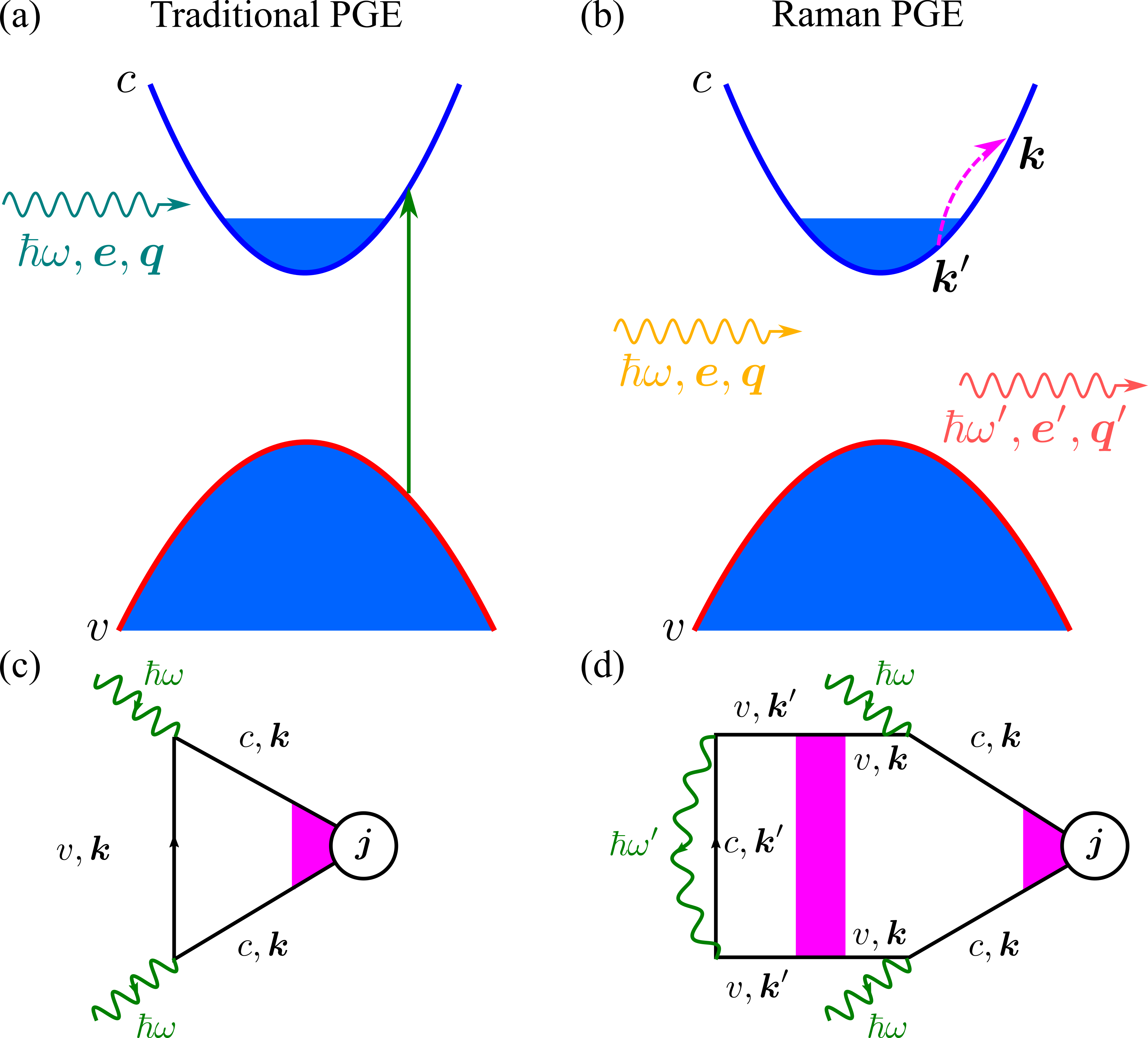
It is commonly assumed that, if the light propagates in the transparency region of the crystal, no dc current is formed [33, 4, 34]. It is indeed the case provided real electronic transitions and corresponding changes of the electromagnetic field are absent in the system. In such a situation, the irradiation results solely in renormalization of the energy dispersion. Thus, after a transient process the current vanishes [33]; otherwise, in violation of the energy conservation law, such current could generate the Joule heating in the external circuit.
Here we show that even in the absence of photon absorption, the dc electric current can be generated if the light is scattered by the free carriers in the medium. The Raman scattering of light leads to the electronic transitions, Fig. 1(b), resulting in the asymmetry of the electron distribution in the steady state and, eventually, in the dc current. A similar idea has been put forward in Ref. [35] without detailed analysis, here we present an explanation of the effect and transparent microscopic model. We develop the microscopic theory of the Raman photogalvanic effect (RPGE) in noncentrosymmetric semiconductors and semiconductor nanostructures. We mainly focus on the case of the circular RPGE where the current reverses its sign under reversal of the radiation helicity. We address the situation where the photon energy is smaller than the fundamental energy gap. We take as examples (i) a non-resonant Raman scattering in bulk semiconductors and (ii) the intersubband resonant Raman scattering in quantum wells.
General description. We recall that the dc current linear in the radiation intensty arising in the non-centrosymmetric media can be written in the most general form as [4, 5]
| (1) |
where is the complex polarization vector of the incident electromagnetic field, with being the circular polarization degree and being the unit vector along the light propagation axis describes the light helicity. Tensors and describe circular and linear photocurrents, respectively; are the Cartesian components. Notably, the first and second terms in Eq. (1) have different properties under time reversal, . Particularly, since both current and light helicity change their signs at the time reversal, tensor is even and the tensor is odd at .
We assume that the light propagates in the transparency region of the direct-gap semiconductor
| (2) |
where is the frequency of radiation, is the band gap, and is the conduction electron momentum scattering time. Here, for definiteness, we assume that the system is -doped. First condition in Eq. (2) ensures that the real interband transitions are forbidden, while the second one allows us to neglect the intraband Drude-like absorption.
Under condition (2) absorption of light is absent and the only possible real processes are the free-carrier light scattering as illustrated in Fig. 1(a). The incident photon with the frequency , polarization , and wavevector scatters and gives rise to a secondary photon with the frequency , polarization and wavevector while a resident electron undergoes a transition from the to state. Thus, the dc current density can be readily expressed as
| (3) |
with the ballistic
| (4a) | |||
| and shift | |||
| (4b) | |||
contributions, respectively [4, 5, 36, 37]. Here is the electron charge, is the normalization volume, is the velocity operator and is the electron density matrix calculated in the second-order in the incident electromagnetic field amplitude. In Eqs. (4), factors ‘2’ account for the spin degeneracy, is the electron dispersion, is the equilibrium Fermi-Dirac distribution function, is the electron velocity, is the probability of electron scattering at the incident light polarization averaged over the polarization and propagation direction of the final photon, and is the electron shift at the quantum transition .
The lack of the inversion center allows for odd in the electron wavevector terms in and even in the wavevector terms in the . It makes contributions (4) non-zero. The contribution (4a) has a clear physical interpretation: In the course of quantum transitions electrons acquire an ‘‘average’’ velocity depending on the light polarization. The velocity generation rate is given by the rate of electron transitions and the velocity relaxation rate is given by the momentum relaxation rate . As a result, the dc current according to this mechanism is formed during the ballistic propagation of electrons between the scattering events and given by the balance of the generation and relaxation processes [4]
| (5) |
The shift photocurrent in Eq. (4b) can be estimated in the same manner with the replacement in Eq. (5) by the ‘‘average’’ shift of the wavepacket in the course of scattering [4]. Equation (5) underlies that the current generation requires real electronic transitions and can be expressed via the light intensity and the extinction coefficient related to the scattering process .
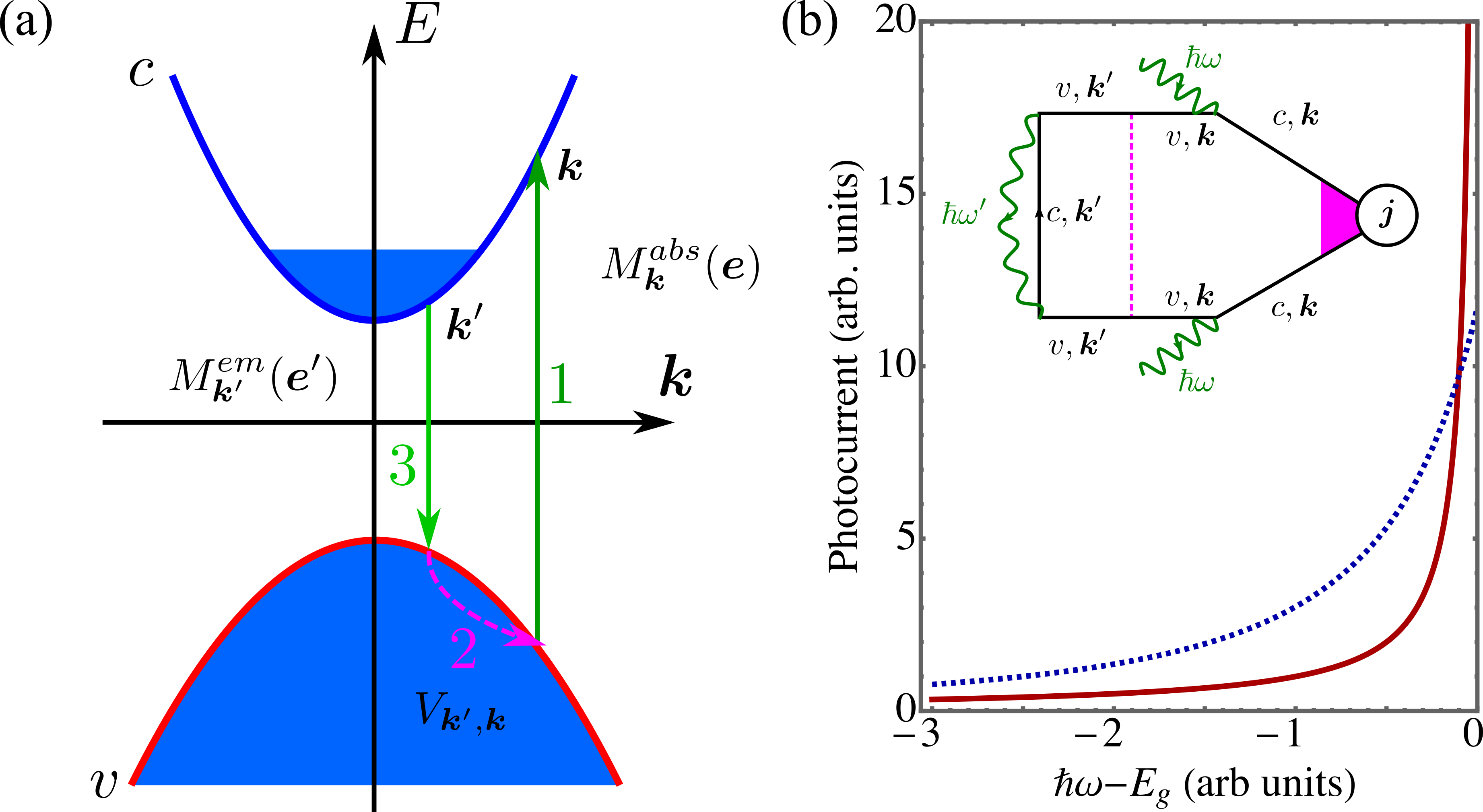
Microscopic model of the impurity or phonon-assisted RPGE. Now we turn to the microscopic description of the scattering processes. We focus on the photocurrent generation process in the bulk gyrotropic semiconductor under assumption that the incident photon energy is smaller but close to the fundamental bandgap . In this situation the main contribution to the free-carrier scattering of light is provided by virtual states in the valence band [5]. Accordingly, the scattering can be described as a three-stage process, where as shown in Fig. 2(a) (i) the incident photon is absorbed (virtually) and creates an electron-hole pair by promoting the electron with the wavevector from the valence band to the conduction band; (ii) the hole in the valence band scatters (by phonon or impurity) in such a way that the state in the valence band becomes filled with electron and the state with the wavevector becomes unoccupied; and (iii) the hole recombines with the resident electron, so that finally the valence band remains unperturbed (all the states are filled) and in the conduction band the state with the wavevector is empty and the state with the wavevector is filled. The corresponding scattering rate is given by
| (6) |
where and are the interband transition matrix elements describing the absorption and emission of photons, respectively. It is convenient to present
| (7) |
where the real second-rank tensor is responsible for the gyrotropy of the system [4] and is a constant. The presence of -linear terms in Eq. (7) makes an odd in the wavevector contribution to the electron transition rate and eventually results in the non-zero photocurrent, Eq. (4b). Equations (4a) and (6) correspond to the diagram in Fig. 2(b). Assuming that the carrier’s momentum relaxation is caused by short-range impurities, introducing as the ratio of the conduction and valence band elastic scattering matrix elements squared and as the radiative decay rate of the photoexcited electron-hole pair we obtain the following expression for the circular photocurrent (see SI for details of derivation)
| (8) |
Here is the electron density in the conduction band, with and being the electron and hole effective masses, and . In derivation of Eq. (8) we assumed degenerate electrons with their Fermi energy . The photocurrent in Eq. (8) increases with decreasing the detuning because the smaller is the more efficient is the light scattering, see Fig. 2(b).
The ballistic photocurrent (8) changes its sign at reversal of the radiation helicity and Eq. (8) describes the circular RPGE. To obtain the ballistic linear RPGE one has to go beyond the three-stage process described above and take into account additional scattering processes to ensure the correct properties of the current under time reversal or evaluate the shift contribution, Eq. (4b), see Ref. [38] for evaluation of for multiquantum transitions. In any case, the linear RPGE will have an additional smallness , , depending on the particular mechanism of the effect.
It is worth to mention that the main contribution to the Raman scattering of light by free charge carriers in semiconductors does not require an additional transition of the hole in the valence band. The electron wavevector can change due to the variation of the light wavevector in the course of scattering
| (9) |
see SI for details. This process is described by the diagram analogous to that in Fig. 2(b) but without the dashed vertical line. Calculation shows that the resulting photocurrent differs from that derived above in Eq. (8) by a factor of . The smallness of such contribution is related to the fact that, in the absence of additional scattering of the hole, the initial and final wavevectors of electrons are close to each other, see Eq. (9): The electron wavevector cannot change more than by a radiation wavevector. It results in a significant reduction of the effect.
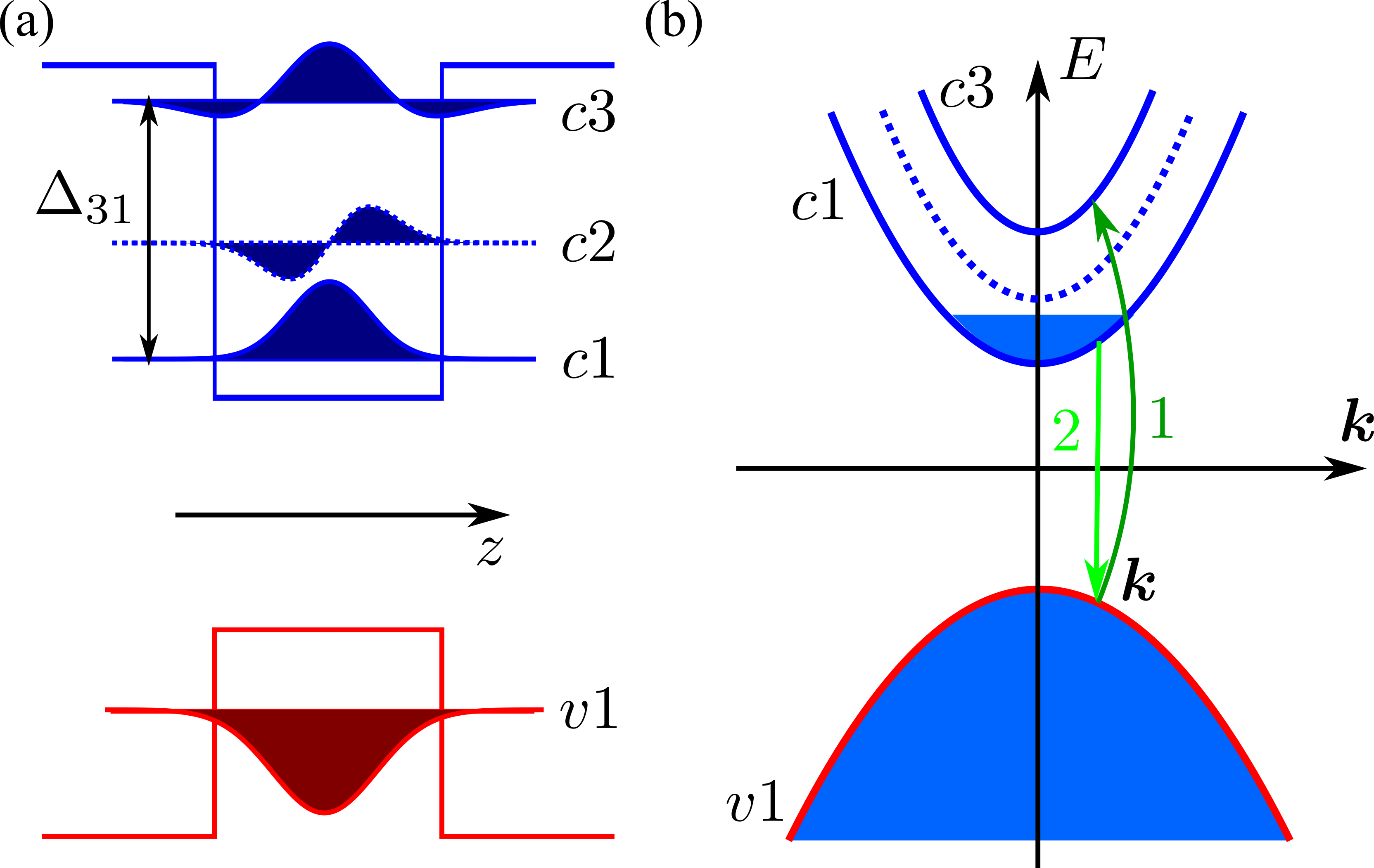
RPGE at the intersubband resonance in quantum well structures. Additional specifics of Raman scattering of light appears where the change of the photon frequency corresponds to a frequency of a resonant excitation in the system. Such situation can naturally arise in quantum well structures as shown in Fig. 3 under conditions of the intersubband scattering [5]. We consider for simplicity a symmetric structure with lowest occupied conduction subband (). As before the frequency of incident photon corresponds to the transparency region of the structure, Eq. (2) and in this case corresponds to the gap between the topmost valence subband and the bottom conduction subband . A situation of interest occurs in the vicinity of the intersubband resonance
| (10) |
where the process depicted in Fig. 3(b) becomes possible. In this case the virtual photon absorption via electron transition is followed by the photon emission process resulting from the transition. As a result, an electron is promoted from subband (in asymmetric quantum wells similar transitions involving subband are also allowed). Corresponding transition rate is readily evaluated [cf. Eq. (6)]
| (11) |
We neglect the photon momentum and any additional phonon or impurity scattering processes, hence the transitions take place at the same electron wavevector . As above we focus on the ballistic circular RPGE because it dominates the photocurrent and using the same Eq. (7) for as in the bulk case we arrive at the following expression for the current density (see SI for details):
| (12) |
Here is the recombination rate of the electron in subband with the hole, we assumed the parabolic dispersion , with () being the effective mass in the th subband, and being the intersubband energy gap. In Eq. (12) we have introduced , is the momentum scattering time of electron at a Fermi surface, the detuning for quantum wells , and
| (13) |
Equation (12) is valid for degenerate electrons and under assumption that the momentum relaxation in the subband is much faster than in subband: It is typically the case because of optical phonon emission processes causing electrons to relax to the bottom subbands; the general case is considered in the SI. It follows from Eq. (12) that RPGE current at intersubband scattering tends to a constant at the absorption edge being much weaker function of the detuning as compared to the analogous photocurrent in the bulk, cf. Eq. (8) and Fig. 2.
Comparison with circular PGE in the absorption region. It is instructive to compare the results for the circular photocurrent obtained here for the transparency region with the well-known results for the circular PGE at the direct interband transitions. Considering the bulk semiconductor in the model described above [see diagram in Fig. 1(c)] we obtain the following expression for the conduction electron photocurrent at :
| (14) |
Here is the absorption coefficient of the semiconductor, the electron momentum scattering time is taken at the energy , and in the case of direct optical transitions. One can recast Eq. (8) in a similar form via the extinction coefficient
| (15) |
with . The factors , , as a result for the same value of detuning the traditional and Raman photocurrents differ by the factor which provides an estimate of the ratio of the electronic transition rates at the light absorption and scattering, respectively. Naturally, both expressions can be brought to the form of general Eq. (5) with
| (16) |
Equations (5), (15), and (16) demonstrate that even for transparent media, real electronic transitions should occur to enable the photocurrent 111Further details and comparison with recent Refs. [35, 42] are presented in SI..
We also note that in gyrotropic semiconductors and nanostructures -linear terms are present in the effective Hamiltonian of the charge carriers due to the spin-orbit coupling [40, 5, 41, 7]:
| (17) |
where is the electron spin operator. These terms provide an additive mechanism for the RPGE current generation. It can be also described by the general Eq. (5) with .
Conclusion. We have shown that the light scattering results in the steady state current in noncentrosymmetric media. The RPGE current is generated even if the light is propagating in the transparency spectral region of the crystal. While absorption is absent in this case, the current results from real electronic transitions owing to the Raman scattering of photons by free charge carriers. These transitions cause asymmetric distribution of electrons and also quantum shifts. We have identified key mechanisms of the Raman scattering induced circular photocurrent for the photon energies slightly below the band gap of a semiconductor and studied the photocurrent generation under intersubband scattering in quantum well structures.
Acknowledgements. We are grateful to Y. Onishi for valuable discussions. The authors acknowledge support from RSF: Project 22-12-00211 (general theory of RPGE, M.M.G.) and 22-12-00125 (calculations of RPGE currents, L.E.G.). L.E.G. also thanks the Foundation for the Advancement of Theoretical Physics and Mathematics ‘‘BASIS’’.
References
- Glass et al. [1974] A. M. Glass, D. von der Linde, and T. J. Negran, High-voltage bulk photovoltaic effect and the photorefractive process in LiNbO3, Applied Physics Letters 25, 233 (1974).
- Ivchenko and Pikus [1978] E. Ivchenko and G. Pikus, New photogalvanic effect in gyrotropic crystals, JETP Lett. 27, 640 (1978).
- Belinicher [1978] V. Belinicher, Space-oscillating photocurrent in crystals without symmetry center, Physics Letters A 66, 213 (1978).
- Sturman and Fridkin [1992] B. I. Sturman and V. M. Fridkin, The photovoltaic and photorefractive effects in non-centrosymmetric materials (Gordon and Breach, New York, 1992).
- Ivchenko [2005] E. L. Ivchenko, Optical spectroscopy of semiconductor nanostructures (Alpha Science, Harrow UK, 2005).
- Ganichev and Prettl [2003] S. D. Ganichev and W. Prettl, Spin photocurrents in quantum wells, J. Phys.: Condens. Matter 15, R935 (2003).
- Dyakonov [2017] M. I. Dyakonov, ed., Spin physics in semiconductors, 2nd ed., Springer Series in Solid-State Sciences 157 (Springer International Publishing, 2017).
- Glazov and Ganichev [2014] M. M. Glazov and S. D. Ganichev, High frequency electric field induced nonlinear effects in graphene, Physics Reports 535, 101 (2014).
- Moore and Orenstein [2010] J. E. Moore and J. Orenstein, Confinement-induced Berry phase and helicity-dependent photocurrents, Phys. Rev. Lett. 105, 026805 (2010).
- Morimoto and Nagaosa [2016] T. Morimoto and N. Nagaosa, Topological aspects of nonlinear excitonic processes in noncentrosymmetric crystals, Phys. Rev. B 94, 035117 (2016).
- de Juan et al. [2017] F. de Juan, A. G. Grushin, T. Morimoto, and J. E. Moore, Quantized circular photogalvanic effect in Weyl semimetals, Nature Communications 8, 15995 (2017).
- Golub et al. [2020] L. E. Golub, E. L. Ivchenko, and B. Spivak, Semiclassical theory of the circular photogalvanic effect in gyrotropic systems, Phys. Rev. B 102, 085202 (2020).
- Orenstein et al. [2021] J. Orenstein, J. Moore, T. Morimoto, D. Torchinsky, J. Harter, and D. Hsieh, Topology and symmetry of quantum materials via nonlinear optical responses, Annual Review of Condensed Matter Physics 12, 247 (2021).
- Ganichev et al. [2008] S. D. Ganichev, W. Weber, J. Kiermaier, S. N. Danilov, P. Olbrich, D. Schuh, W. Wegscheider, D. Bougeard, G. Abstreiter, and W. Prettl, All-electric detection of the polarization state of terahertz laser radiation, Journal of Applied Physics 103, 114504 (2008).
- Danilov et al. [2009] S. N. Danilov, B. Wittmann, P. Olbrich, W. Eder, W. Prettl, L. E. Golub, E. V. Beregulin, Z. D. Kvon, N. N. Mikhailov, S. A. Dvoretsky, V. A. Shalygin, N. Q. Vinh, A. F. G. van der Meer, B. Murdin, and S. D. Ganichev, Fast detector of the ellipticity of infrared and terahertz radiation based on HgTe quantum well structures, Journal of Applied Physics 105, 013106 (2009).
- Asnin et al. [1978] V. M. Asnin, A. A. Bakun, A. M. Danishevskii, E. L. Ivchenko, G. E. Pikus, and A. A. Rogachev, Observation of a photo-emf that depends on the sign of the circular polarization of light, JETP Letters 28, 24 (1978).
- Ganichev et al. [2001] S. D. Ganichev, E. L. Ivchenko, S. N. Danilov, J. Eroms, W. Wegscheider, D. Weiss, and W. Prettl, Conversion of spin into directed electric current in quantum wells, Phys. Rev. Lett. 86, 4358 (2001).
- Ganichev et al. [2002] S. Ganichev, E. Ivchenko, and W. Prettl, Photogalvanic effects in quantum wells, Physica E: Low-dimensional Systems and Nanostructures 14, 166 (2002).
- Wittmann et al. [2010] B. Wittmann, S. N. Danilov, V. V. Bel'kov, S. A. Tarasenko, E. G. Novik, H. Buhmann, C. Brüne, L. W. Molenkamp, Z. D. Kvon, N. N. Mikhailov, S. A. Dvoretsky, N. Q. Vinh, A. F. G. van der Meer, B. Murdin, and S. D. Ganichev, Circular photogalvanic effect in HgTe/CdHgTe quantum well structures, Semiconductor Science and Technology 25, 095005 (2010).
- McIver et al. [2012] J. W. McIver, D. Hsieh, H. Steinberg, P. Jarillo-Herrero, and N. Gedik, Control over topological insulator photocurrents with light polarization, Nature Nanotechnology 7, 96 (2012).
- Olbrich et al. [2014] P. Olbrich, L. E. Golub, T. Herrmann, S. N. Danilov, H. Plank, V. V. Bel’kov, G. Mussler, C. Weyrich, C. M. Schneider, J. Kampmeier, D. Grützmacher, L. Plucinski, M. Eschbach, and S. D. Ganichev, Room-temperature high-frequency transport of Dirac fermions in epitaxially grown Sb2Te3- and Bi2Te3-based topological insulators, Phys. Rev. Lett. 113, 096601 (2014).
- Plank et al. [2016] H. Plank, L. E. Golub, S. Bauer, V. V. Bel’kov, T. Herrmann, P. Olbrich, M. Eschbach, L. Plucinski, C. M. Schneider, J. Kampmeier, M. Lanius, G. Mussler, D. Grützmacher, and S. D. Ganichev, Photon drag effect in (Bi1-xSbx)2Te3 three-dimensional topological insulators, Phys. Rev. B 93, 125434 (2016).
- Durnev and Tarasenko [2019] M. V. Durnev and S. A. Tarasenko, High-frequency nonlinear transport and photogalvanic effects in 2D topological insulators, Annalen der Physik 531, 1800418 (2019).
- Leppenen and Golub [2022] N. V. Leppenen and L. E. Golub, Nonlinear optical absorption and photocurrents in topological insulators, Phys. Rev. B 105, 115306 (2022).
- Ma et al. [2017] Q. Ma, S.-Y. Xu, C.-K. Chan, C.-L. Zhang, G. Chang, Y. Lin, W. Xie, T. Palacios, H. Lin, S. Jia, P. A. Lee, P. Jarillo-Herrero, and N. Gedik, Direct optical detection of Weyl fermion chirality in a topological semimetal, Nature Physics 13, 842 (2017).
- Rees et al. [2020] D. Rees, K. Manna, B. Lu, T. Morimoto, H. Borrmann, C. Felser, J. E. Moore, D. H. Torchinsky, and J. Orenstein, Helicity-dependent photocurrents in the chiral Weyl semimetal RhSi, Science Advances 6, eaba0509 (2020).
- Drexler et al. [2013] C. Drexler, S. A. Tarasenko, P. Olbrich, J. Karch, M. Hirmer, F. Muller, M. Gmitra, J. Fabian, R. Yakimova, S. Lara-Avila, S. Kubatkin, M. Wang, R. Vajtai, P. Ajayan, J. Kono, and S. D. Ganichev, Magnetic quantum ratchet effect in graphene, Nature Nanotechnology 8, 104 (2013).
- Candussio et al. [2021a] S. Candussio, M. V. Durnev, S. Slizovskiy, T. Jötten, J. Keil, V. V. Bel’kov, J. Yin, Y. Yang, S.-K. Son, A. Mishchenko, V. Fal’ko, and S. D. Ganichev, Edge photocurrent in bilayer graphene due to inter-Landau-level transitions, Phys. Rev. B 103, 125408 (2021a).
- Candussio et al. [2021b] S. Candussio, L. E. Golub, S. Bernreuter, T. Jötten, T. Rockinger, K. Watanabe, T. Taniguchi, J. Eroms, D. Weiss, and S. D. Ganichev, Nonlinear intensity dependence of edge photocurrents in graphene induced by terahertz radiation, Phys. Rev. B 104, 155404 (2021b).
- Quereda et al. [2018] J. Quereda, T. S. Ghiasi, J.-S. You, J. van den Brink, B. J. van Wees, and C. H. van der Wal, Symmetry regimes for circular photocurrents in monolayer MoSe2, Nature Communications 9, 3346 (2018).
- Rasmita et al. [2020] A. Rasmita, C. Jiang, H. Ma, Z. Ji, R. Agarwal, and W. bo Gao, Tunable geometric photocurrent in van der waals heterostructure, Optica 7, 1204 (2020).
- Asgari and Culcer [2022] R. Asgari and D. Culcer, Unidirectional valley-contrasting photocurrent in strained transition metal dichalcogenide monolayers, Phys. Rev. B 105, 195418 (2022).
- Belinicher et al. [1986] V. I. Belinicher, E. L. Ivchenko, and G. E. Pikus, Transient photocurrent in gyrotropic crystals, Sov. Phys. - Semicond. 20, 558 (1986).
- Golub and Ivchenko [2018] L. E. Golub and E. L. Ivchenko, Circular and magnetoinduced photocurrents in Weyl semimetals, Phys. Rev. B 98, 075305 (2018).
- Onishi et al. [2022] Y. Onishi, H. Watanabe, T. Morimoto, and N. Nagaosa, Photovoltaic effect in noncentrosymmetric material without optical absorption, arXiv: 2204.12727 (2022).
- Belinicher et al. [1982] V. I. Belinicher, E. L. Ivchenko, and B. I. Sturman, Kinetic theory of the displacement photovoltaic effect in piezoelectrics, JETP 56, 359 (1982).
- Sturman [2020] B. I. Sturman, Ballistic and shift currents in the bulk photovoltaic effect theory, Physics-Uspekhi 63, 407 (2020).
- Golub and Ivchenko [2011] L. E. Golub and E. L. Ivchenko, Shift photocurrent induced by two-quantum transitions, JETP 112, 152 (2011).
- Note [1] Further details and comparison with recent Refs. [35, 42] are presented in SI.
- Rashba and Sheka [1959] E. I. Rashba and V. I. Sheka, Symmetry of energy bands in crystals of wurtzite type. II. Symmetry of bands with spin-orbit interaction included, Fiz. Tverd. Tela: Collected Papers 2, 162 (1959).
- Ganichev and Golub [2014] S. D. Ganichev and L. E. Golub, Interplay of Rashba/Dresselhaus spin splittings probed by photogalvanic spectroscopy – A review, physica status solidi (b) 251, 1801 (2014).
- Shi et al. [2022] L. Shi, O. Matsyshyn, J. C. W. Song, and I. S. Villadiego, The Berry dipole photovoltaic demon and the thermodynamics of photo-current generation within the optical gap of metals, arXiv: 2207.03496 (2022).