Diamond Integrated Quantum Photonics: A Review
Abstract
Integrated quantum photonics devices in diamond have tremendous potential for many quantum applications, including long-distance quantum communication, quantum information processing, and quantum sensing. These devices benefit from diamond’s combination of exceptional thermal, optical, and mechanical properties. Its wide electronic bandgap makes diamond an ideal host for a variety of optical active spin qubits that are key building blocks for quantum technologies. In landmark experiments, diamond spin qubits have enabled demonstrations of remote entanglement, memory-enhanced quantum communication, and multi-qubit spin registers with fault-tolerant quantum error correction, leading to the realization of multinode quantum networks. These advancements put diamond at the forefront of solid-state material platforms for quantum information processing. Recent developments in diamond nanofabrication techniques provide a promising route to further scaling of these landmark experiments towards real-life quantum technologies. In this paper, we focus on the recent progress in creating integrated diamond quantum photonic devices, with particular emphasis on spin-photon interfaces, cavity optomechanical devices, and spin-phonon transduction. Finally, we discuss prospects and remaining challenges for the use of diamond in scalable quantum technologies.
I Introduction
Quantum technology has come a long way since the Stern–Gerlach experiment was conducted a century ago[2]. Developments in quantum theory have provided the foundation for much of present-day technology, including, but not limited to, lasers, atomic clocks, and techniques in medical imaging, and have the potential to impact diverse fields spanning computing[3, 4], communication[5, 6], and sensing[7, 8, 9]. We are now at an exciting moment where early-stage quantum computers have demonstrated quantum advantage[10, 11, 12, 13], quantum-secured communication has been demonstrated over intercontinental distances[14, 15], and quantum sensors have surpassed the sensitivity limits defined by the laws of classical physics[16].
A cornerstone for the development of real-world quantum applications is the resilient and scalable interconnection of different quantum systems. While several proof-of-principle experiments have been conducted with trapped atoms and ions[17, 18, 19, 20, 21, 22, 23, 24, 25], scaling to a larger quantum system remains a challenge, in-part due to the complex laser trapping techniques required. Solid-state systems offer the possibility to adapt nanofabrication capabilities developed by the semiconductor industry to mass-produce quantum devices[26]. Superconducting quantum circuits[27], gate-defined quantum dots[28], and semiconductor spin qubits[29] all take advantage of scalable nanofabrication to create quantum information processing devices. Integrated photonic devices could play a key role in these efforts by harnessing light’s ability to transmit quantum information, and are becoming increasingly important as quantum technologies mature. Diamond has emerged as a promising material for photonic quantum systems build around artificial atoms formed by impurities in the diamond crystal[30]. These atomic-scale impurities are optically active, allowing them to the controlled and connected through photonic channels, and to be interfaced with other photonic quantum technologies.
In recent decades, the development of photonic quantum technologies[31] has expanded the quantum information ecosystem, particularly in the fields of quantum communication and quantum sensing. Quantum communication has many potential applications, including clock synchronization[32] and encrypted communication[33, 34]. Central to these applications is a quantum photonic network enabling the transmission and entanglement of quantum bits (qubits) over long distances[35].
To realize a quantum network, remote quantum network nodes must be entangled via quantum links. As illustrated in Fig. 1 (a), these network nodes are small-scale quantum processors that combine robust storage of quantum information with an interface to the quantum communication channels[36]. The nodes must enable high-fidelity operations on several entangled qubits and fault-tolerant multi-qubit protocols[37]. Furthermore, the nodes need to be capable of storing quantum states utilizing ‘memory’ qubits for a longer time than is required to generate asynchronous entanglement across numerous distant nodes. An additional requirement for network nodes is the realization of a fast and efficient interface between stationary qubits and ‘flying’ photonic qubits. For long-distance communication, the flying qubits must have minimal losses in the photonic quantum channel, thus limiting the use to telecom photons that are compatible with pre-existing low-loss optical fiber networks[38, 39, 35].
Optically active spin-qubits in diamond have successfully been utilized in several proof-of-principle experiments targeted towards the integration of the above mentioned components to realize a quantum network[40, 41, 42, 43, 44]. Advances in spin-photon entanglement[45] paved the way for photon-mediated entanglement of remote qubits[46, 47, 48], culminating in the recent demonstration of a three-node quantum network[49, 50]. While these demonstrations have been fruitful, it is worth noting that parallel advances have been made with other experimental platforms including trapped atoms and ions[18, 51, 52, 53, 54, 55], superconducting resonators[56, 57], self-assembled quantum dots[58, 59, 60], and defect-based qubits in other wide-bandgap semiconductors and dielectrics[61, 62, 63, 64, 65, 66, 67, 68, 69, 70, 71].
Realizing an efficient interface between diamond qubits and photons at telecommunication wavelengths for fiber-based quantum channels remains a significant hurdle as diamond-based qubits do not intrinsically couple to telecom photons. The optically active spin qubits found in diamond typically emit photons in the visible range, thus requiring quantum frequency conversion to telecom wavelengths[72] to mitigate absorption loss in fiber optic links[35]. The need for optical frequency conversion, however, can be circumvented by taking inspiration from the development of quantum transducers[73] and utilizing the mechanical properties of diamond in combination with device engineering[74]. Diamond is the stiffest material known to man with Young’s modulus exceeding 1,200 GPa[75], facilitating the fabrication of high-frequency mechanical resonators[76, 77]. These mechanical resonators have the potential to be universal quantum transducers[78, 79], capable of coupling a myriad of different quantum systems, including connecting superconducting qubit resonators and optical photons[80, 81]. Photon-phonon and subsequent spin-phonon coupling in a mechanical resonator constitute a promising route to realize a spin-photon interface natively operating at telecom wavelengths[82, 74, 83]. Furthermore, the high mechanical frequencies of these diamond resonators suppress the population of thermal phonons, facilitating preparing of the mechanical resonator to the quantum ground state.
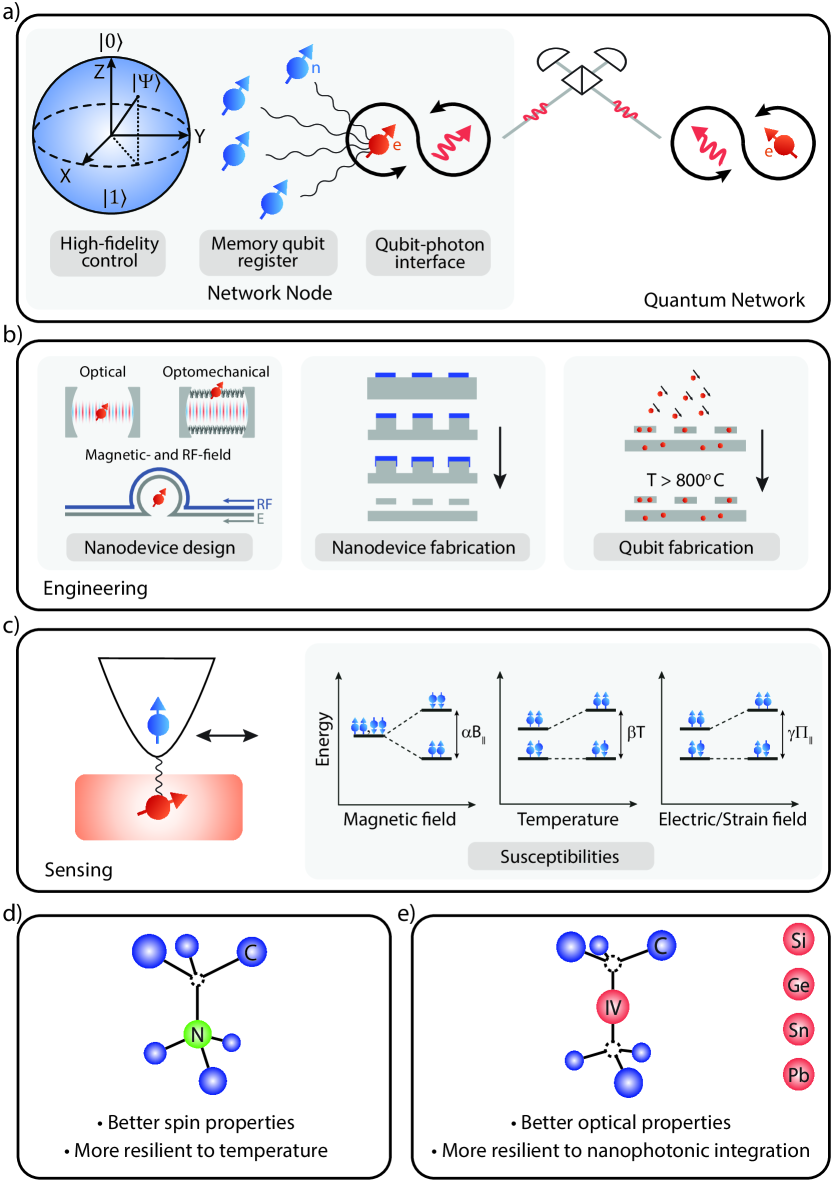
Unleashing diamond’s full potential as a material platform for quantum information processing is impaired by two preeminent challenges: deterministic creation of highly coherent qubits and scalable device fabrication. A key requirement for scaling beyond a few qubits is the precise fabrication of arrays of identical qubits separated by a few nanometers, a level of precision required to magnetically couple the electron spins to mediate multi-qubit operations[84, 85, 86]. Significant progress has been achieved in ‘top-down’ qubit fabrication techniques, however it remains challenging to meet the necessary requirements[87]. A promising approach to overcome this obstacle is ‘bottom-up’ atomically-precise fabrication that has been successfully demonstrated in silicon[88]. Alternatively, proposals for coupling qubits via a quantum optical bus require devices that combine deterministic creation of qubits with quantum control via externally applied fields[89], such as optical, stress, magnetic, and radio and microwave frequency electric fields, see Fig. 1 (b). The engineering of these control mechanisms requires robust device fabrication. Utmost care needs to be taken during device fabrication as the qubits are intrinsically sensitive to their surrounding environment and their properties can be degraded by their proximity to surfaces[90]. However, by turning the problem around, their sensitivity to their environment (see Fig. 1 (c)) can be exploited to realize quantum sensors[9] that offer advantages over their classical counterparts. Diamond-based sensors are being developed at a rapid pace and offers to fill the gap created by other candidates in terms of resolution, portability, and cost.
In this article, we focus on recent developments in the field of diamond integrated photonics and its impact on the quantum technology ecosystem. The article is organized as follows: In Sec. II we introduce the physics and the strengths and weaknesses of diamond colour centers. In Secs. III and IV, we provide an overview of the recently developed field of diamond cavity optomechanics and discuss the potential of photon-phonon coupling for quantum technology in diamond. In Secs. V, VI, VII, and VIII, we review the current state-of-the-art, discuss open questions, and provide a roadmap unravelling the promising future for diamond nanofabrication, quantum photonic devices, sensing and metrology, and qubit-photon interfaces.
II Color centers in diamond
Diamond, an inherently transparent material, is host to over 200 optically active defect centers[91, 92]. These defects, known as color centers, can occur naturally or be created in the lab (see Sec. V-C). Some color centers combine atom-like optical transitions with long-lived electron spins, resembling ions trapped in the diamond lattice[93]. Diamond’s large electronic bandgap () and resulting wide transparency window and large energy separation between colour center energy levels and the crystal’s conduction and valance bands, combined with a low population of thermal phonons (Debye temperature[94, 75]) promotes coherent single-photon emission and long spin coherence times, making diamond an ideal host for solid-state qubits. Furthermore, the diamond lattice is largely composed of nuclear spin-0 12C atoms (natural abundance ), thus suppressing background magnetic noise. Synthetic growth of diamond using isotopically purified starting material further reduces magnetic noise, leading to prolonged spin coherence times[95]. The electron spin associated with color centers may be utilized as a qubit that, when interfaced with photons, can form part of a quantum network node. Furthermore, coupling to nearby long-lived nuclear spins[96] can be harnessed to build quantum memories[97] and multi-qubit spin registers[98]. Entanglement swapping between the electron spin and the long-lived nuclear quantum memory[99, 41], can free up the communication qubit, enabling high-fidelity multi-qubit protocols[100]. For scalability, it is desirable to position the memory qubit in close spatial proximity to the communication qubit; a challenging task using 13C spins owing to the low natural abundance of only [101]. As an alternative, a quantum memory can be realized using the nuclear spins intrinsic to the color center[101]. This latter approach carries the advantage that the memory qubit is automatically located adjacent to the communication qubit[102].
Being robust single-photon sources[103, 104], the nitrogen-vacancy (NV)[105] and silicon-vacancy (SiV)[106] centers have over the years gained traction as promising candidates for a variety of applications in photonic quantum technologies[107, 30]. NV centers have been used in various proof-of-principle experiments, including, but not limited to quantum sensing[108], quantum teleportation[40], quantum error correction[109, 84, 110], demonstration of a multi-qubit quantum processor with coherence times approaching a second for the electron spin[111] and a minute for the nuclear spin[98], fault-tolerant operations[37], and the realization of multinode quantum networks[49, 50]. On the other hand, SiV centers integrated with nanophotonic structures with exceptionally large cavity cooperativities have been used to demonstrate memory-enhanced quantum communication[43]. In addition, novel color centers based on the heavier group-IV atoms such as germanium (Ge), tin (Sn), and lead (Pb), show promising potential for quantum applications[112]. However, research on these defects is still in the early stages and will therefore not be discussed extensively in this review.
II-A Defect Structure
The NV center, depicted schematically in Fig. 1 (d), consists of a substitutional nitrogen atom and an adjacent lattice vacancy with the symmetry axis along the crystal direction. The group-IV atoms, on the other hand, are too large to occupy a carbon site. Instead, the impurity atom takes up an interstitial position, flanked by a vacancy on either side[113, 114]. This split-vacancy configuration, with the group-IV atom positioned at the inversion point of the diamond lattice, is shown schematically in Fig. 1 (e). The centrosymmetric configuration results in a vanishing permanent electric dipole moment, rendering the group-IV color centers insensitive to linear Stark shifts[115, 116]. The unpaired electrons associated with the neutral charge states, NV0 and XV0, where X refers to one of the group-IV atoms in Fig. 1 (e), can efficiently capture an electron from the environment, forming the negative charge states, NV- and XV-, respectively[117, 118]. The negative charge state is the most studied for both classes of defects. However, it is worth mentioning that for the SiV center, careful doping and surface treatment have stabilized the neutral charge state SiV0[119, 120]. Similar results are yet to be reported for the heavier group-IV defects. Therefore, in the context of this review, we will be referring to the negative charge states, unless explicitly stated otherwise.
| Color center | (nm) | Radiative lifetime (ns) | Quantum efficiency | Debye–Waller factor | GS (Hahn-echo) | Spin-strain coupling (per strain) | Orbital-strain coupling (per strain) |
| NV- | 637 | 85 | 0.033 | 1.7 ms4 (RT, 69 mT) | 21.5 GHz5 (GS; RT) 290 GHz5 (ES; 10 K) | 1 Hz5 (ES; 10 K) | |
| SiV- | 7386 | 7 | 1-10 | 0.79 | 0.3 ms10 (0.1 K, 160 mT) | N /A † | 1 PHz11 (GS; mK) |
II-B Spin and Optical Properties
The NV center ground-state manifold is composed of an orbital singlet, spin-triplet state ()[133], where, for zero magnetic field, the and the spin sub-levels are split by due to spin-spin interactions[105]. For the group-IV split-vacancies, the ground-state manifold is an orbital-doublet state, where spin-orbit interactions split the orbital branches by [118, 132]. As will be discussed below, the value of directly determines the spin coherence times. A comparison between the key spin and optical properties for the NV and SiV center is summarized in Table I.
As a direct consequence of the difference in symmetry (Fig. 1 (e)-(f)) and corresponding energy level structure, the NV and SiV centers exhibit different spin and optical properties, in turn determining in which areas they find applications. Due to the weak spin-orbit coupling[134] and the largely spin-free diamond lattice[95], the NV center electron spin is only weakly coupled to its environment, resulting in exceptionally long spin-lattice relaxation times () and spin-coherence () at room temperature[75]. The long spin coherence time makes the NV center a workhorse in quantum sensing applications across a broad temperature range[135, 136]. The SiV center, on the other hand, suffers from relatively short spin coherence times. In the case of the SiV center, the spin coherence time is limited by phonon-assisted population transfer between the two orbital branches (split by GHz), resulting in coherence times limited by the orbital time[132, 137, 138]. Cooling down to millikelvin temperatures suppresses the thermal phonon population, thereby increasing the spin coherence time[130]. SiV coherence time-scales are typically in the range of 100 ns at room temperature, extendable to a few ms at millikelvin temperatures, thus limiting the potential sensing applications of SiV centers.
The observation of two-photon quantum interference from spatially separated emitters[139, 140, 141], a prerequisite for remote entanglement protocols[46, 47], requires coherent emission of indistinguishable photons. For NV centers, the photon flux is limited by the long radiative lifetime of . Furthermore, emission into the zero-phonon line (ZPL) at , quantified by the Debye-Waller (DW) factor, accounts for only of the total emission[123]: the remaining is accompanied by phonons, resulting in a broad phonon-sideband (PSB) extending to . The SiV center, on the other hand, exhibits a comparatively short radiative lifetime of [126, 127]. Moreover, of the emitted photons are directed along the ZPL at [118, 129]. However, the SiV center suffers from a low quantum efficiency (QE) of only [128, 127] compared to a near-unity QE for the NV center[122].
In brief, the large difference in the DW factor between NV and SiV centers can be attributed to the symmetry of the defect[134]. In the case of the NV center, excitation from the ground-state (GS) to excited-state (ES), denoted by and , respectively[133], shifts the charge distribution towards the N atom[142, 143]. This charge redistribution alters the equilibrium position of the nuclei, resulting in a reduced overlap between the ground- and excited vibronic states manifested by a large PSB[105, 134]. In comparison, the charge distribution between the ground () and excited state () of the SiV center remains similar; there is little change in the nuclear equilibrium coordinates. Consequently, optical emission from the SiV center occurs largely into the ZPL[134, 113].
For both families of color centers, the presence of a magnetic field lifts the ground-state spin degeneracy: the spin sub-levels can be individually addressed using externally applied microwave[144, 145, 130] or strain fields[146, 147, 131], enabling the formation of a qubit. Furthermore, both defects exhibit cycling optical transitions, enabling all-optical spin control[148, 149] and single-shot spin-readout[150, 130] at cryogenic temperatures.
III Coherent Photon-Phonon Coupling in Diamond: Cavity Optomechanics
Initial efforts to integrate diamond qubits with photonic devices have focused on photon-spin coupling, as discussed in previous reviews[151, 152] and addressed later in this review. Recently, efforts to harness spin-phonon coupling in diamond for realizing both on-chip and long-distance quantum coherent connections between diamond spin qubits have emerged[75, 153]. Central to these efforts is the field of cavity-optomechanics, which can provide coherent photon-phonon coupling in integrated photonic devices. Cavity optomechanics[154, 155], has enabled quantum technologies in fields including sensing and precision measurement, studies of the quantum properties of mechanical objects, quantum memories, and quantum transduction. It has been investigated in a plethora of materials and designs, and has recently been shown to be a viable and promising route to control and read out spin qubits in diamond[74]. This latter demonstration harnesses the convenient frequency matching between mechanical resonances of integrated devices and solid-state qubit spin transitions.
Cavity optomechanical systems use two distinct mechanisms to create and enhance the interaction between the optical field in a cavity and mechanical resonators: moving mechanical boundaries[156] and photoelasticity[157]. The mechanical displacement of vibrating cavity walls drives the moving boundary effect, whereas the photoelastic effect is a bulk response that manifests as strain-induced modulation of the refractive index. These light-matter interactions are quantified through the single-photon optomechanical coupling rate, , calculated as the product of the optical frequency shift per unit displacement and the mechanical zero-point fluctuation amplitude of a mechanical resonator mode of interest. Experimental determination of , in general, is realized by the parametric fitting of well-known optomechanical (OM) effects, such as the optical spring effect and the optomechanical (anti-) damping. A direct measure of is possible by comparing the OM transduction with an artificial phase-modulated tone, a method commonly used and described by Gorodetsky et al.[158]. These measurements are corroborated by numerical simulations utilizing perturbation theory and the finite element method (FEM)[159].
To be used in quantum applications, optomechanical cavities must be designed to achieve high while also overcoming optomechanical losses. This requirement is characterized by the optomechanical cooperativity, given by:
| (1) |
Here, and are the energy decay rates of the cavity’s optical and mechanical modes of interest, respectively, and is the average intracavity photon number. can be interpreted as the probability of coherent OM interaction[160]. The condition has been realized in a variety of cavity OM devices, including those fabricated from diamond[77, 76]. Moreover, quantum state transfer between light and mechanics that can generate entanglement between photons and phonons demands devices with , where is the average thermal phonon number of the mechanical resonator due to its thermal bath[161, 162]. Lowering either requires cooling resonators to cryogenic temperatures, using high-frequency resonators, or a combination of both. Another condition that is key to many applications is reaching the sideband-resolved regime, that is, when the resonator’s mechanical mode frequency exceeds , facilitating delayed optical back-action that can be harnessed for optical amplification or cooling of mechanical resonance.
The above discussion only accounts for the real part of the optomechanical coupling. In cases where the change in a cavity’s optical losses via mechanical displacement is significant, will be defined as a complex quantity with dispersive and dissipative contributions[159]. Furthermore, when the device is operated under high optical power, dynamic and static photothermal and thermoelastic effects may be relevant, which can significantly modify the physics of the problem[163, 164, 165]. In this review, we focus on the dispersive OM interaction; the above-mentioned effects are neglected unless explicitly stated.
III-A Relevant material properties
A fortuitous combination of exceptional intrinsic material properties is responsible for making diamond an ideal material for cavity optomechanics. Advances in the synthetic growth of single-crystal diamond (SCD) combined with the development of fabrication techniques to realize suspended structures from high-quality SCD chips have accelerated the recent emergence of diamond nanophotonic and nanomechanical devices for quantum technologies. Diamond’s key material properties relevant to quantum photonics are outlined below.
Optics
The strong covalent bond of diamond hinders electrical conductivity, resulting in a wide bandgap of 5.47 eV (225 nm). This large bandgap creates a broad transparency window ranging from ultraviolet to radio frequencies, except for a weak absorption window appearing between 2.6 and 6.2 m due to multi-phonon coupling[166]. Outstanding transparency, when combined with a high refractive index of 2.4 and low dispersion, makes diamond a robust and versatile medium to confine photons. Additionally, the large bandgap suppresses multi-photon absorption, providing the ability to handle large optical power inside a cavity with minimal nonlinear absorption and resulting thermal effects, unlike other popular semiconductors such as silicon and gallium arsenide[167].
While thermal nonlinear effects are mostly undesirable, optical nonlinearities lead to interesting physics. Diamond’s lowest-order non-zero nonlinear susceptibility, , allows the study of phenomena such as Raman scattering[168, 169, 170], the Kerr effect[171, 172], and four-wave mixing[173]. Amid many prospects, the on-chip demonstration of diamond-based microcombs[174], Raman lasers[175, 176], and single-photon frequency conversion via a combination of parametric processes with color centers are among the most promising[177].
Special attention must be paid to surface termination, which can introduce additional losses when device dimensions reach the nanoscale. A high concentration of impurities, such as color centers, may have an impact on both optical and mechanical loss rates. Even though diamond is an optically isotropic material due to its cubic lattice symmetry, the strain induced by the presence of impurities can cause birefringence.
Mechanics
Diamond has exceptional mechanical properties. It has a high Young’s modulus of 1220 GPa, four times larger than silicon, making it a stiff material with a large speed of sound (18,000 m / s). The large stiffness facilitates the fabrication of high-frequency resonators by reducing reliance on small geometry, ameliorating access to mechanical resonances resonant with a wide range of spin qubit transition frequencies. Equally important, diamond is a material with low intrinsic mechanical dissipation. In general, the predominant geometry-independent dissipative channels for nanomechanical semiconductor resonators near room temperature are thermoelastic damping and phonon-phonon scattering[178]. Both these effects are temperature-dependent, and therefore, their contribution is relatively small in diamond due to its high thermal conductivity (2,200 W / mK, several times higher than copper) and density (3,500 kg /m3), alongside its low thermal expansivity. At cryogenic temperatures, scattering by defects such as dangling bonds, intrinsic or extrinsic dopants, and lattice imperfections can dominate phonon losses[179]. Such interactions are commonly modelled as strain waves coupling to two-level systems and might be the ultimate limit for achieving ultra high-Q nanomechanical resonators[180].
Besides the lattice anisotropy introduced by defects, even undoped SCD is an imperfect isotropic elastic material. Although the anisotropy level is often disregarded without penalty, fine tailoring of diamond’s mechanical properties is sometimes necessary. Huang et al.[181] have demonstrated that Young’s modulus varies depending on the crystal orientation. Likewise, other properties such as photo-elasticity are also influenced by the crystallographic direction, as demonstrated in gallium arsenide[157]. These variations can be accounted for by a thorough description of the diamond elasticity tensor[182, 183].
III-B Experimental realizations of diamond optomechanical devices
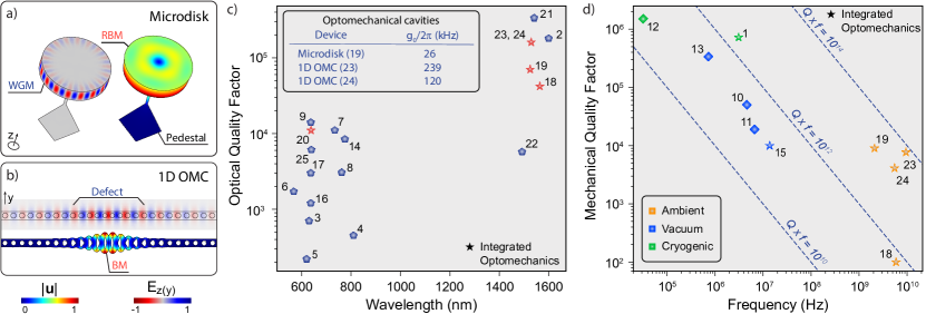
Efforts to utilize optical fields to manipulate and probe micro-and nano-scale mechanical objects have led to numerous types of optomechanical devices[155]. Amongst these, microdisk resonators are one of the simplest optical cavity designs and play an important role in many photonics and optomechanics experiments. Microdisks support optical whispering gallery modes (WGM), in which the electromagnetic field is confined by total internal reflection at the circular boundary (Fig. 2 (a)). The mode volume of WGMs decreases with decreasing microdisk radius, while optical radiation loss increases. An optical quality factor of at telecommunication wavelengths was achieved in 5 diameter SCD microdisks by Mitchell et al.[200], limited by fabrication related surface roughness. At visible wavelengths resonant with NV optical transitions, have been observed in SCD microdisks[76].
Optomechanical microdisks are supported by small pedestals that minimize anchor losses, as shown in Fig. 2 (a). Optical WGMs couple most effectively to mechanical radial breathing modes (RBM): resonances with mechanical frequency GHz, mechanical quality factor , and kHz have been reported for a diamond microdisk[76]. This device demonstrated at ambient conditions, enabling a number of coherent optomechanics experiments, including reversible photon-phonon conversion via optomechanically-induced transparency[202, 203], phonon-mediated wavelength conversion[204], and optomechanical memory[203]. These demonstrations took advantage of the multimode nature of the diamond microdisk; a topic that will be discussed in Sec. IV.
The advantages of microdisk resonators go beyond their ease of fabrication and effective OM interaction. Usually, resonators with small dimensions are targeted due to their low effective modal mass, leading to a higher and larger . Tuning of the device geometry modifies the optical free spectral range (FSR) and can enable mechanical frequencies ranging from kHz to GHz – such design flexibility is favorable for coupling to spin qubits[153]. On the downside, mechanical quality factors are highly dependent on the disk-to-substrate interconnection. While M. Mitchell et al.[76] demonstrated the feasibility of fabricating a thin pedestal in diamond microdisks, the patterning of a nanostructured phononic shield on the top of the disk could provide a solution to further isolate clamping and reduce anchor losses[205, 206].
Optomechanical crystals (OMC) are another device design used to simultaneously confine optical and mechanical modes[207]. Their sophisticated engineering allows for small optical mode volumes and high OM coupling rates compared to other geometries. The basic principle involves introducing a geometric defect in an artificially patterned lattice (Fig. 2 (b)) that generates periodicity in the dielectric constant and elastic properties of a material. This in turn modifies the dispersion of photonic and phononic modes of the structure. These defects are generally implemented by alternating air and material regions, for example by introducing air holes in a suspended film. The resulting photonic and phononic band structures have regions with vanishing density of states. Introducing defects that break the lattice’s translational symmetry allows the formation of localized optical and mechanical resonances at frequencies within the bandgaps of the respective optical and photonic band structures. Additionally, these modes can simultaneously have low radiation and clamping losses, respectively, by ensuring that the defect minimizes the coupling to the lossy modes of the underlying periodic structure[208].
Diamond photonic crystal cavities (PCC) and nanomechanical resonators were first explored independently. Photonic crystal optical cavities using triangular nanobeam PCCs were demonstrated with a [188], soon followed by a due to advances in fabrication techniques[186]. Rectangular cross-section photonic crystal cavities[189] better suited for integration into a larger photonic integrated circuit have been demonstrated using quasi-isotropic undercutting of SCD with [192]. These rectangular cross-section cavities minimize the mixing of the TE and TM optical modes which can be responsible for optical loss in triangular cross-sections[188].
Photonic crystal cavities fabricated using heteroepitaxy of diamond on silicon[187] or diamond membrane transfer[193] have . Two-dimensional PCCs, have been realized from diamond films bonded or deposited over a different material substrate. They can currently reach optical -factors of a few thousand[187, 195, 196, 197]. Recently, quasi-isotropic etching[209] was used to realize 2D photonic crystals with [198]. Several of the aforementioned devices have been realized with cavities in the visible wavelength range, as shown in Fig. 2 (c).
The realization of SCD nanomechanical resonators has made steady progress in recent years, as illustrated in Fig. 2 (d). Cantilevers with dimensions suspended over a SiO2 substrate have been demonstrated with a in vacuum[199], while Tao et al.[179] reported that similar structures made from SCD film in a ‘quartz sandwich’ can achieve . These high- cantilevers have also been used to investigate the relevance of surface termination and defect concentration. In Ref.[185] both singly- and doubly-clamped nanobeams showed in angle-etched SCD.
Khanaliloo et al.[184] demonstrated one-dimensional suspended waveguides in SCD supporting flexural mechanical modes with . Polycrystalline diamond nanobeams and H-resonators with have been connected to nanophotonic circuits[210, 195]. Cady et al.[194] have fabricated diamond OMCs using a SCD-on-insulator platform with integrated telecom waveguides with and GHz mechanical modes with . Burek et al.[77] fabricated and measured a 1D OMC with a , and kHz. These realizations demonstrate that diamond cavity optomechanics has enormous potential. However, the fabrication of smooth sidewalls and the precise etching of small periodic features in diamond OMCs are currently major obstacles to further experimental progress, as will be discussed in Sec. V.
IV Multimode Optomechanics
The majority of cavity optomechanics studies utilize systems with a single optical mode coupled to one mechanical mode. As discussed, an asset of diamond cavities is their ability to support optical modes across a wide transparency window, thus facilitating the study of multimode optomechanics, where multiple optical modes are coupled to the same mechanical mode (see Fig. 3 (a, left)). Similarily, mechanical resonators typically support a spectrum of modes that can couple to a single optical mode (see Fig. 3 (a, right)). Constraining the physics to the ‘one-to-one’ model is often justified and dictated by the experimental design. For example, cooling or heating in the resolved sideband regime singles out a particular mechanical mode via the choice of laser detuning[211].
Setups with multimode coupling have been realized in a wide range of materials[212] and have a number of additional valuable features[213, 214, 215, 216, 217, 218]. For example, bulk acoustic modes in a macroscopic scale quartz cavity have been used to demonstrate optomechanically induced transparency and absorption[219]. Multiple mechanical modes coupled to an optical mode have demonstrated a cascaded optical transparency scheme by leveraging the parametric phonon–phonon coupling with an aluminium nitride microwheel resonator[220], coherent optomechanical state swapping between two spatially and frequency separated resonators with silicon nitride trampoline resonators[221], and multimode phonon lasing with a 1D silicon optomechanical crystal cavity[222]. Furthermore, exploring multimode systems in synchronized OM oscillator arrays constitutes an interesting approach for sensing and metrology[223].
Multimode cavity optomechanical devices also offer great potential to connect disparate quantum technologies in a network, via phonon-mediated coherent transduction of quantum information from visible or microwave photons to telecommunication wavelengths. As such, the field of optical-to-microwave transduction[224] is currently a highly active area of research[225]. Optomechanical systems with are capable of frequency conversion between multi-wavelength cavities[226, 227, 204], eliminating the need for material-dependent nonlinear optical processes. Cavity optomechanical wavelength conversion coherently couples two optical cavity modes via their independent optomechanical coupling to a common mechanical resonance[226, 204].
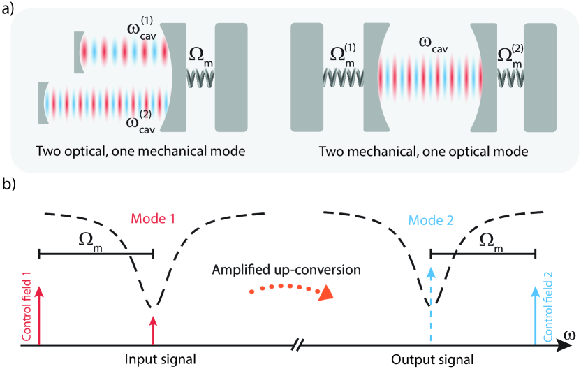
In diamond, optomechanical cavities have been used to demonstrate wavelength conversion between frequencies separated by over 4 THz with an internal efficiency of 45 [204]. For wavelength up- and down-conversion, both strong optical control fields are typically red-detuned by the mechanical frequency from cavity modes resonant with each wavelength of interest. However, blue detuning of one of the control fields can be harnessed for optomechanically amplified wavelength conversion, as illustrated in Fig. 3 (b). Dynamics in both of these wavelength conversion schemes can be modelled by a photon-phonon beamsplitter or squeezing Hamiltonians[154]. These systems can, in principle, be utilized to convert the zero phonon line emissions from NV and SiV centers in diamond to telecom photons for application in quantum networks, provided the cavity supports high- optical modes at both the photon emission wavelength and the telecom wavelength of interest, and that can be achieved for each mode. However, these advancements are currently limited due to modest at visible wavelengths. Advances in fabrication techniques and better cavity design can overcome this problem, see Sec. V. Coupling higher intensity control fields to the cavity at the visible wavelength in order to achieve larger will also increase .
Other multimode optomechanical phenomena with promising quantum applications have been demonstrated in diamond devices enabled by double-optomechanically induced transparency (DOMIT). Examples include all-optical two-color switching[228] and optomechanicaly tunable pulse storage[203]. Recently, optical modes were used to drive a broad mechanical mode spectrum of diamond microdisks. In this work, higher-order mechanical modes with frequencies over 10 GHz were observed. Devices with one optical and multiple mechanical modes could lead to many interesting studies, as already demonstrated in the microwave domain[229], but have not yet been explored in SCD optomechanical systems. Hybrid SCD cavity optomechanical devices integrated with superconducting quantum devices could accelerate the realization of transducers for connecting superconducting quantum computers to quantum networks[78].
V Diamond Nanofabrication
Advances over the last decade in the fabrication of nanostructures from single-crystal diamond (SCD) have accelerated the development of components necessary for fully integrated quantum photonics platforms. These components, engineered to enhance light-matter interactions, play a crucial role in the fields of cavity optomechanics (see Sec. III and IV), nanophotonics (see Sec. VI), and qubit-photon interfaces (see Sec. VIII). They include, but are not limited to, single-photon sources based on color-centers[92], wave-guiding structures[230], optical[231, 197] and mechanical resonators[76, 194], and optical fiber-based / free-space couplers[190, 232, 233]. In this section, the challenges of SCD nanostructuring are briefly introduced, followed by discussions of top-down fabrication methods for bulk diamond, as well as methods for creating color centers in these structures.
V-A Single-Crystal Diamond Fabrication Challenges
In addition to diamond’s ability to host color centres, its allure for nanophotonic and nanomechanical applications derives from the advantageous material properties of diamond introduced above (see Sec.III-A). The unit cell of SCD consists of two diagonally inter-penetrating face-centered cubic lattices where each carbon atom is purely covalent-bonded to its four nearest-neighbours with tetrahedral symmetry. This atomic structure grants diamond its unique mechanical, thermal, and optical properties, including the wide transparency window and chemical inertness[166].
Although these properties make SCD an excellent material for integrated photonic devices, they also provide significant challenges in nanostructuring. Traditional top-down nanofabrication approaches rely on lithographic patterning of masking material, and subsequent etching steps to define photonic and mechanical components. The high chemical inertness of diamond limits etching chemistries to processes involving oxygen plasma, while the strong bonding nature of the carbon atomic lattice makes physical etching, such as focused ion beam milling, difficult. Currently, high-quality SCD in thin-film form, where a refractive index contrast confines light within the film thickness, is not commercially available, although recent progress has been made in hetero-epitaxially grown films on various substrates[234]. Though polycrystalline thin-films are readily available, they might not be suitable for hosting quantum emitters due to the presence of dopants and grain boundaries[166, 235]. Several paths have been taken in order to overcome these challenges, both in etch mask development and through the use of different SCD precursor materials, ranging from thinned membranes to bulk substrates.
V-B Creating suspended structures in bulk diamond
High-quality, commercially available SCD in bulk form, grown on diamond templates via chemical vapour deposition (CVD), is a popular precursor material for diamond nanostructuring. Both optical and electronic grade forms of CVD diamond, with the latter having less than 10 parts per billion in residual nitrogen density, are available down to millimeter-scale substrate form. The substrate surfaces are mechanically polished (a specialized procedure that is often outsourced) to sub-nanometer RMS surface roughness. Initial cleaning of the substrates typically uses a boiling piranha solution (3:1 ratio of sulfuric acid and hydrogen peroxide) for approximately 15 minutes, followed by a rinse in water and drying with a nitrogen gun. These steps can be supplemented with a combination of a hydrofluoric acid dip for 5 minutes and sonication in acetone and or methanol[236]. Optical microscopy inspection of the substrate post-cleaning should yield a clean surface, absent of graphitic or other residues, often evident as dark spots. If not, the cleaning process should be repeated. In cases where the substrates have been treated with high-temperature annealing or ion irradiation, the induced graphitic or pyrolytic carbon residue can be etched in a tri-acid cleaning solution (a boiling mixture of nitric, sulfuric, and perchloric acids), though care should be taken with the associated risks in this potentially volatile process.
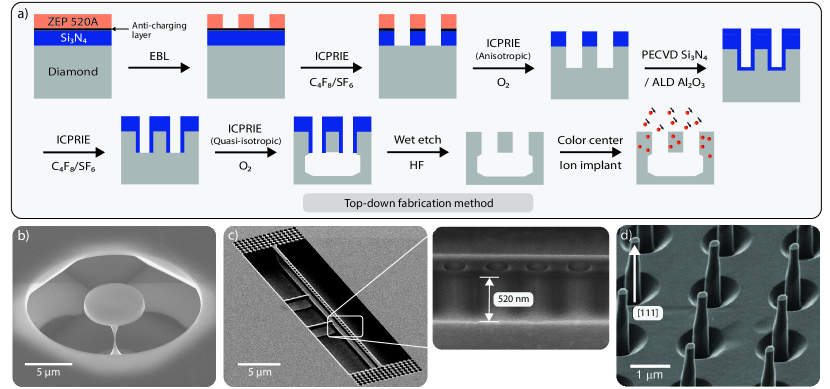
Perhaps the most challenging aspect of diamond nanostructuring lies in identifying a mask material with sufficiently high selectivity to oxygen-based plasma etching, in order to withstand pattern transfer into the substrate. Polymer resists commonly used in electron beam (or photo-) lithography are not sufficient, and therefore an additional hard mask layer is required. A common choice for a hard mask is silicon nitride (Si3N4) deposited by plasma-enhanced chemical vapor deposition (PECVD) with a thickness of about 250 nm for anisotropic etches into diamond of several micrometers[209, 192, 231, 200, 184]. The process flow is schematically outlined in Fig. 4 (a). After hard mask deposition, a thin (5 nm) conductive film is deposited onto the substrate in order to provide a charge compensating layer during the electron beam lithography (EBL). This is required due to the highly insulating nature of diamond. There are several options for use as the anti-charging layer including evaporated amorphous carbon, titanium, and niobium, with the latter two providing secondary functionality as an adhesion layer between diamond and the resist[237]. After spin-coating and baking the resist, patterning is performed with EBL followed by resist development. In the case of positive-tone resists (such as PMMA or ZEP 520A) where scission of polymer chains occurs during development, cooling of the developer to around -10∘C will yield improved pattern and line edge resolution[238]. The pattern in the developed resist is transferred to the nitride layer using an inductively coupled plasma reactive ion etch (ICPRIE) with C4F8 / SF6 chemistry, followed by an anisotropic oxygen plasma etch to transfer the pattern to the diamond substrate. Alternatively, negative-tone HSQ electron beam resists can be patterned directly on the diamond. Patterned HSQ has an oxide-like nature that is resistant to oxygen plasma etching[237].
Quasi-isotropic diamond undercut etching can then be used to create suspended diamond devices. This technique, which was inspired by the silicon SCREAM fabrication process[239], has been adopted in numerous studies[192, 240, 200, 241, 242]. It requires that the sidewalls of the diamond nanostructure to be protected. A conformal layer of silicon nitride deposited using a similar procedure as in the application of the initial hard mask, or an Al2O3 layer created by atomic layer deposition[198], has been used for sidewall shielding. The horizontal surfaces of the protective layer are removed preferentially using an anisotropic ICPRIE etch, leaving the sidewalls covered while exposing the diamond surfaces to be etched. The undercutting of the devices uses a zero DC-bias quasi-isotropic oxygen etch[209] at elevated temperatures of 200-300∘C to increase the vertical and horizontal etch rates, which are dependent on the diamond crystal facet orientations in the bulk substrate. Finally, the residual resist and the hard mask are removed in a hydrofluoric acid wet etch. Representative devices fabricated using this process in the geometries of a microdisk and one-dimensional photonic crystal cavity beam are shown in Figs. 4 (b) and (c), respectively.
Two alternative approaches for creating free-standing structures from bulk single-crystal diamond are reactive ion beam angled etching (RIBAE)[243, 237] and Faraday cage angled reactive ion etching[244]. In RIBAE, an incident beam normal to the substrate surface defines the depth of the nanostructure through a lithographically patterned mask. The substrate is then tilted, such that the ion beam is at an acute angle to the substrate surface and etching occurs under rotation, yielding suspended nanostructures with a triangular cross-section. In Faraday cage angled etching, a Faraday cage surrounding the sample is used to redirect the RF field driven ions in the plasma.
V-C Color Center Fabrication
A common feature for the color centers discussed in Sec. II is the presence of an impurity atom combined with adjacent lattice vacancies. However, for many quantum applications, a high-quality diamond with a low concentration of impurities is desired to mitigate electric- and magnetic noise caused by impurity ions. Both the impurity atom and the vacancies can be introduced in various ways. For example, vacancies can be introduced by irradiation of high-energy particles, such as electrons, neutrons, and ions, or via intense, ultrafast laser pulses (see the last panel, Fig. 4 (a))[245, 246, 247, 248]. High-temperature annealing () provides sufficient thermal activation energy for the vacancies to diffuse. During this diffusion process, the vacancies can combine with impurity atoms, forming color centers. The annealing is usually carried out in a high vacuum or in an inert atmosphere to avoid the etching of the diamond surface and the formation of a graphitic surface layer[249]. The bombardment of particles during irradiation leads to crystal damage–a potential source of paramagnetic noise adversely affecting the spin and optical properties of the color centers. In principle, annealing mitigates these noise sources by repairing the crystal damage[250].
For the integration of color centers in devices such as photonic cavities[231, 123] and all-diamond scanning probes[251], precise control of the lateral and vertical position of the color centers with respect to the relevant fields involved is of paramount importance. In principle, this can be accomplished by deterministically fabricating the devices around the color centers–a challenging task with the current state-of-the-art fabrication techniques. Another way to remedy this problem is to introduce impurity ions via -doping. This technique has been successfully demonstrated for nitrogen-vacancy centers by introducing nitrogen gas during the CVD diamond growth process[252, 253]. The depth of the doping layer is controlled by the subsequent diamond overgrowth[252, 254]. The aforementioned irradiation and thermal annealing techniques can then be used to form NV centers in -doped diamond.
Contrary to nitrogen, silicon is rarely found in natural diamond[253]. However, silicon doping is readily achievable during diamond growth, for example by the incorporation of SiO2 or SiC into the growth chamber[126] or by introducing silane (SiH4) gas during the growth process[255, 256]. Similarly, the introduction of germane (GeH4) gas allows the formation of GeV centers[257].
Alternatively, impurity ions can be incorporated into the diamond post-growth via ion implantation. Here, the implantation aids the formation of vacancies, which, during thermal annealing, can form color centers[248]. Ion implantation has successfully demonstrated the creation of NV centers[258, 259], SiV centers[260, 261], GeV centers[262], SnV centers[263, 264] and PbV centers[265, 266]. However, the large size of the heavy group-IV atoms leads to greater lattice damage and larger strain in the crystal after thermal treatment[267]. However, shallow implantation and subsequent diamond overgrowth[268] allow for the creation of deep group-IV defects while maintaining a crystalline environment.
For ion-implanted samples, spatial positioning can, in principle, be achieved by implanting through an AFM tip[269, 196], by the use of lithographically defined masks[102, 270] or using focused ion beam (FIB)[271, 272]. Furthermore, the ion implantation energy can be adjusted according to the desired target depth, allowing for the creation of color centers at a depth ranging from a few to several tens of nanometers. In particular, the use of FIB allows for high-precision implantation into pre-fabricated photonic structures, such as photonic crystals[273] and nanobeam cavities[127, 42, 272]. However, the creation of deeper color centers requires the use of high-energy ions. These ions lose energy in collision with electrons and atomic nuclei in the lattice, thereby leading to a trail of lattice damage along the trajectory[274]. Furthermore, the collision with nuclei causes deviation from the designated path, thereby reducing the spatial accuracy.
Vacancy generation using tightly focused, ultrafast laser pulses constitutes a promising alternative to ion implantation for the creation of NV centers deep in the diamond[275, 276]. In this process, vacancies are formed as a consequence of optical breakdown caused by tunnelling or multiphoton absorption[277]. The highly nonlinear nature of this process confines the lattice damage within the focal volume of the excitation laser[278]. Relying on the natural occurrence of nitrogen in electronic grade diamond (), laser writing and subsequent annealing has led to the formation of highly stable NV centers[275, 279, 280]. The creation of stable SiV centers has been demonstrated by coating the diamond surface with silicon nanoballs followed by fs laser illumination[281].
For quantum sensing applications (see Sec. VII), it is necessary to have the probe spin in close proximity to the target spins[282, 283, 284]. The reason is twofold: firstly, magnetic dipolar coupling of probe spin with the nearby target spins scales as , where is the probe-to-target spin distance. Consequently, only in the nanometer range can provide sufficient coupling strengths. Secondly, for imaging applications the spatial resolution is determined by the minimum , thus demanding close proximity of the probe and target spins, which is even more critical since the targets often lie exterior to the diamond surface. Clearly, only probe spins located a few nanometers below the diamond surface are useful for such applications. However, these so-called shallow spins are also extremely sensitive to various unwanted noise sources present on the surface, thereby severely degrading their spectral and spin properties[285, 286, 90]. In this regard, engineering robust sensing qubits is an ongoing endeavour.
VI Quantum Photonic Devices
Efficient collection of photoluminescence (PL) is of paramount importance for applications using color centers in diamond. However, the large refractive index of diamond () leads to total internal reflection at the diamond-air interface, limiting the detection efficiency to only a few for color centers in bulk diamond when using a high numerical aperture microscope[287]. To remedy this problem and improve the photon flux, a variety of different micro- and nano-photonic devices have been fabricated on diamond[288].
VI-A Efficient Photon Extraction via Device Fabrication
A widely adopted approach for improving the collection efficiency of broadband PL from color center is fabricating solid immersion lenses (SILs, see Fig. 5 (a))[287, 289]. PL emitted from a color center located in the focus of the SIL will strike perpendicular to the diamond surface, thus suppressing total internal reflection. SILs have been used to demonstrate enhanced detection efficiency from NV centers[150, 290], SiV centers[126, 118] and GeV centers[291, 292]. One key advantage of SILs is their relatively easy fabrication using FIB milling around pre-characterized color centers located deep in the diamond. This is of particular importance for experiments using NV centers, where the proximity to surfaces often deteriorates their optical coherence[90]. State-of-the-art demonstrations of remote entanglement of NV centers[46, 47] utilized diamond SILs fabricated around naturally occurring NV centers[274]. Diamond SILs provide a detection efficiency of [293], which can be further improved by the application of an anti-reflective coating[40].
Although diamond SILs suppress total internal reflection, the photon detection efficiency is still limited by the non-directional emission of the color center PL. Recently, it has been demonstrated that the detection efficiency can be further increased by using layered dielectric optical antennas[294]. Such a device combines layers of different dielectric materials, where the contrast in refractive index modifies the emission pattern, leading to preferential photon emission into the high-index material[295]. In the context of diamond photonics, a low-loss, broadband dielectric antenna has been demonstrated using a diamond micromembrane () bonded to a macroscopic GaP SIL () suspended in air ()[296]. As a consequence of the asymmetric refractive index profile, PL is predominantly emitted into the GaP. The hemispherical shape of the SIL suppresses total internal refraction, and can thus, in principle, provide a near-unity collection efficiency[297, 298]. An alternative approach constitutes the use of inverse design[232] to fabricate photonic structures. Recently, this approach demonstrated a 14-fold enhancement of broadband PL from NV centers located at a depth of 100 nm[233].
Nanophotonic waveguiding structures, such as nanowires[299, 300, 301] and nanopillars (see Fig. 4 (d))[302, 303], offer an alternative method to improve the collection efficiency of broadband PL. These devices act like antennas, directing the emitted PL into a well-defined guided mode[151]. Detection efficiency of has been demonstrated using top-down fabricated nanowires on diamond with ingrown NV centers[299]. One particular advantage of nanopillars is the possibility to embed single color centers close to the tip () by shallow ion implantation (see Section V-C) prior to fabrication, while maintaining long spin coherence times[251, 304]. This is of particular importance for applications in quantum sensing, where the spatial resolution depends on the sensor to sample distance[108]. Tailoring the pillar geometry can further increase the collection efficiency. Recently, a collection efficiency of was demonstrated for an NV center located at the focus of a truncated parabolic reflector diamond nanopillar[305].
VI-B Engineering of the Photonic Environment
The devices discussed so far enhance the collection efficiency of broadband PL, which is particularly useful for applications in quantum sensing, where an increased photon flux leads to improved sensitivity to magnetic fields[108]. However, quantum information applications require a high flux of coherent, indistinguishable photons, and therefore modification of the optical properties of the color centers is often desired. The rate of remote entanglement in schemes relying on two-photon quantum interference is limited by the detection rate of coherent photons. At the time of writing, the current state-of-the-art experiment using NV centers achieved an entanglement rate of [48, 49], limited by the long radiative lifetime (), the aforementioned small branching into the ZPL (Debye-Waller factor of ) and poor photon extraction efficiency owing to total internal reflection. While the group-IV defect centers possess more favorable optical properties in terms of a larger Debye-Waller factor and shorter radiative lifetime, to date, no experiments demonstrating remote entanglement have been conducted, though recently indistinguishable photons from SnV color centers were reported[306].
In principle, these shortcomings can be addressed by embedding color centers in photonic resonators[307]. Resonant coupling of the ZPL to a single cavity mode enhances the ZPL emission on two grounds. First, the cavity directs the emission into a well-defined output mode, improving the photon collection efficiency[308, 309]. Second, the emitter experiences a Purcell effect[310] that enhances the spontaneous emission rate of transitions resonant with a cavity mode. This can be used to increase the fraction of photons emitted into the ZPL[123]. For an optical cavity with quality factor and mode volume , the Purcell factor is given by
| (2) |
where describes the overlap between the dipole moment and the electric field . Note that is independent of any emitter properties– is described solely by the characteristics of the cavity[309]. The scaling motivates the use of high-quality resonators with minimal mode volume[152].
Coupling between color centers in diamond and photonic resonators has been demonstrated on various different platforms[152], including, but not limited to, photonic crystal cavities[311, 197, 187, 312, 313], nanobeam cavities[314, 315, 42, 316, 43, 241, 242], waveguides[317, 230, 318], microrings[231, 319, 320], hybrid optical devices[321, 322, 323, 324, 325, 326] and open microcavities[327, 328, 123, 329, 330, 331, 332].
In photonic crystal cavities (PCC), the periodic change in refractive index creates a photonic bandgap. Tailoring of the periodicity can confine light to a mode volume of . However, at the visible wavelengths relevant for color centers in diamond, imperfection in the fabrication of these devices limits the achievable -factor to . The current state-of-the art PCC containing SiV centers exhibits and [43]. Note that PCCs with have been demonstrated for [186]. As discussed in Section V-C, deterministic coupling of color centers to PCCs can be achieved via FIB milling around pre-characterized color centers[312], or by using a FIB to implant ions in fabricated structures. The latter approach has been proven to be particularly successful for SiV centers[42]. Furthermore, red-shifting of the cavity resonance is possible via deposition of [42] or Ar[241] gas, thereby maximizing the spectral overlap between the color canter ZPL and the cavity mode.
Coupling to WGMs in diamond microdisk- and ring resonators offer a monolithic alliterative to PCCs. In general, WGMs offer a larger -factor, albeit at the expense of a larger . In practice, due to fabrication imperfection and surface roughness, the achievable -factors are comparable to those of PCCs[231]. Nevertheless, due to advances in device fabrication, a diamond microdisk with has been demonstrated for [76].
The monolithic photonic devices discussed above offer large ratios at the expense of invasive nanofabrication. While NV centers with close-to lifetime limited optical linewidths have been reported in bulk[333, 249], NV centers embedded in nanophotonic devices often suffer from poor optical coherence and inhomogeneous broadening of the ZPL linewidth on the account of a fluctuating charge environment caused by fabrication induced surface damage[334, 90]. Therefore, increasing the defect free, crystalline environment has proved to be beneficial[335].
Hybrid photonic platforms constitute an alternative to monolithic resonators on the account of the possibility to use bulk diamond. These devices (see Fig. 5 (b)) combine single-crystal diamond with waveguides and resonators fabricated from a high-index material[336, 337]. Evanescent coupling of NV centers to waveguides[338, 322] and microcavites[321, 339] has been demonstrated on various platforms based on GaP[323]. However, while red-tuning of the cavity resonance are possible via gas deposition, one remaining drawback of these hybrid devices is the difficulty in positioning the color center close to the field maxima of the guided mode[322]. Furthermore, evanescent coupling requires near-surface NV centers, which, as discussed above, suffer from inhomogenous linewidth broadening[90]. Nevertheless, hybrid photonic devices offer a viable route to integrate color centers in diamond with large-scale photonic integrated circuits[340, 341]. The state-of-the-art experiment demonstrated a 128-channel ‘quantum microchiplet’, a diamond waveguide array containing highly-coherent SiV and GeV centers interfaced with an integrated AlN photonic circuit[325].
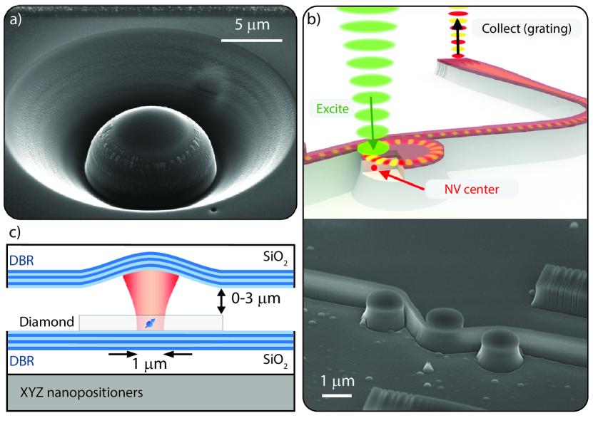
In recent years, planar-concave open Fabry-Perot microcavities (see Fig. 5 (c)) have emerged as a compelling alternative to the monolithic and hybrid optical resonators discussed above[123, 331, 332]. These cavities are formed from a highly-reflective planar distributed Bragg-reflector (DBR), to which a diamond membrane is bonded. A second highly-reflective DBR mirror, with micron-sized concave indentations fabricated using FIB milling[342, 327] or CO2 laser ablation[343, 344, 345], concludes the cavity. The Gaussian-shaped indentations facilitate efficient coupling of the cavity mode to single-mode external detection optics[346, 347]. The open microcavity offers the possibility to incorporate micron-sized single-crystal diamond membranes[348], thus preserving the optical coherence of NV centers[332], while maintaining a large -ratio[309]. Furthermore, with the use of piezoelectric nanopositioners, the open microcavity platform offers full in situ tunability and control of both the cavity resonant frequency and the relative position of the color center with respect to the cavity mode[123]. Resonant coupling of a single NV center to an open microcavity has demonstrated enhancement of the fraction of ZPL photons to [123]. Finally, the incorporation of a diamond membrane with a small thickness gradient has demonstrated full in situ control of both the resonant frequency, and the relative frequency spacing of adjacent cavity modes[349], thus providing a platform for tunable nonlinear optics.
VII Sensing and Metrology
Quantum sensing and metrology involve the detection and measurement of physical quantities using quantum properties such as coherence and entanglement, with the goal of reaching fundamental limits in the measurement[7, 9]. Varieties of such sensors have been developed in the past several decades[9]. Among the solid-state platforms, spins in diamond have emerged as versatile sensors for a variety of physical quantities, both classical and quantum[350]. The NV center outperforms other emitters in diamond primarily due to its excellent spin (e.g. long coherence times) and optical (e.g. photostability, brightness) properties.
VII-A NV Center-Based Sensing
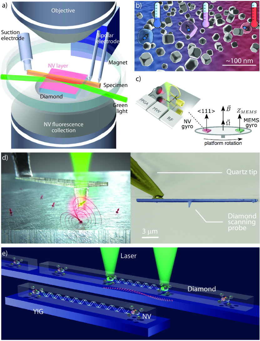
The NV center’s electron spin has proven to be an exquisite probe for measuring several physical quantities, both external and internal to the host diamond, like electric and magnetic fields[9, 351], temperature[352, 353], pressure[354], strain[355], rotation[356], and charge[357] with high sensitivity (see Fig. 6). Diamond based sensing has been intensely pursued and is rapidly progressing owing to the potentially immediate commercial and fundamental interests in physics, chemistry, biology and clinical research[350, 9, 351].
One added advantage of the NV spin as a sensor is its atomic size, which provides extremely high spatial resolution, outperforming any other sensors developed to date[282]. Depending on the application in question, NV-based sensors have been realized using ensembles or single NV centers in diamond nano-, micro-, or bulk crystals[350, 351]. One area where the NV sensors have made a profound impact is the realization of nanoscale nuclear magnetic resonance (NMR) spectroscopy[358] and magnetic resonance imaging (MRI) at ambient conditions and moderate bias magnetic fields[283, 284]. NMR using NV centers has addressed the concerns of the low sensitivities associated with traditional NMR methods[359] and the complexities associated with advanced methods like magnetic resonance force microscopy (MRFM)[360]. Recent advances in NV nano-NMR methods have placed NV centers at the forefront of molecular-scale NMR with unprecedented spectroscopic[358] and structural resolution[361].
For magnetic resonance based methods to work at the level of a single target molecule or atom, the probe has to have sufficient sensitivity to individual spins as well as possess fine spectral resolution. In this regard, NV centers have shown to be sensitive to individual molecules and spins external to the diamond surface. An NV spin, being an atomic scale probe, is capable of measuring NMR signals from target spins in about sample volumes[362, 363] with a sub-Angstrom spatial resolution[364, 361] at ambient conditions. In comparison, traditional NMR requires nanoliter sample volumes and the spatial resolution is limited to m-scale[359], excluding their application to the level of single live cells, for instance. Recent advancements in NV sensing protocols have also allowed the achievement of finer spectroscopic details of the target sample. These approaches include utilizing long-lived nuclear spin lifetimes[365] and quantum heterodyne methods[366, 367, 358] to achieve several orders of magnitude improvement in spectral resolution, effectively bypassing the standard limits set by the and times of NV spin. The demonstrated sensitivities are sufficient to resolve subtle chemical signatures in picoliter sample volumes[358]. In addition, NV centers have shown to be promising sensors in condensed matter[368] and biomagnetism[350, 369], and considerable attempts have been made in using NVs for detecting dark matter[370].
Magnetometers are ubiquitous in many areas of application. The current state-of-the-art magnetometers (e.g. superconducting quantum interference devices or SQUIDs and optically pumped magnetometers or OPM) suffer from non-ambient operating conditions, modest spatial resolution, and limited dynamic range, albeit offering the highest sensitivities. To this end, progress in NV-magnetometers over the last decade has proven to be promising, however, some key challenges remain to be addressed[350, 351]. The primary challenge is that the sensitivities achievable with NV magnetometers are worse than both the theoretical predictions and the competing techniques (SQUIDs and OPMs) by at least three orders of magnitude[9, 351]. This is mainly due to inefficient NV spin readout methods and limited coherence times. For a diamond sample with number of NV sensors per volume (=1 for a single NV center), the magnetic field sensitivity, , scales as[371, 372]
| (3) |
where is the readout fidelity, and is the interrogation time (here, the spin initialization and readout times are neglected). is determined by the PL photon collection efficiency and the contrast of the spin states, both of which are far below unity, thus rendering 1. is limited primarily by the photon shot noise since the readout is performed optically[351], and ultimately by the quantum projection noise, , so that [9]. Several approaches have been explored to improve beyond the limits of standard optical readout by employing non-PL based readout schemes. However, some key challenges remain for all these methods in terms of optimizing the overhead (spin initialization and readout) times, added experimental complexities, and limited readout fidelities. As an alternative to PL detection schemes, cavity-enhanced readout methods, based on the IR absorption by the NV center singlet state[373] and interaction between NV and microwave photons in a resonator[374] have been demonstrated. While these methods have substantially enhanced the fidelity (and hence ) by achieving near unity IR light collection efficiency[373] and unity contrast[374], the overall is still short of reaching the . Further miniaturization of the sensor in these cavity-based systems for high spatial resolution remains challenging due to their mm-lengthscale. In this context, diamond microcavities could fill this gap given their sub-m size, and appreciable ratio (see Sec.VI-B)[209], thus potentially enabling stronger interaction between spins and cavity fields, leading to better . However, it is important to understand the charge state dynamics of the NV centers under extreme optical powers in microcavities as they strongly affect .
The next critical factor influencing is : improves with longer . The nature of the signal that can be probed depends on the characteristic timescales of the sensor spins: their inhomogeneous dephasing time () and spin coherence time (). Short-lived times allow for the detection of only static or slowly varying target -fields such as those in biological samples[369] or condensed matter[368]. On the other hand, long-lived times can probe AC fields or fast oscillations like those from the spins inside[375] and outside diamond crystal[362, 363]. Engineering qubits with maximum and directly affects quantum sensing strategies involving phase accumulation, and is therefore currently one of the major material fabrication challenges.
The remaining parameter influencing is . However, arbitrarily increasing degrades the and times due to enhanced dipolar interaction among the sensing spins (NV-NV) and with substitutional nitrogen spins[376]. Another drawback of sensing using a large is the compromise of a key advantage of the NV center spin: its atomic spatial resolution. Currently, the best-reported are in the range of T (for DC)[371] and nT (for AC)[95, 377] for a single NV, and about pT (DC and AC) for an ensemble NV sensor[351, 378].
In summary, a crucial challenge to realize diamond as a robust quantum sensor performing at its fundamental limits lies in achieving unity readout fidelities and engineering high-quality, affordable, diamond samples with prolonged coherence times. From a material engineering point of view, a complete understanding and mitigation of the undesired surface-induced noise sources are essential for sensing target signals. Ongoing investigations on the novel color centers in diamond may overcome the challenges posed by NV centers as a sensor.
VII-B Hybrid Diamond-Magnetic Sensors
A related area of research that could benefit from the properties of diamond constitutes the development of nano-optomechanical torque sensors, which have demonstrated enhanced sensitivities to mechanical torque[379, 380, 16]. They naturally respond to the fundamental interaction of magnetic moments with an external field–the magnetic torque–at a magnitude proportional to the total magnetization[381] providing insight into the dynamics of nanomagnetic structures.
The coupling of magnetic and mechanical systems has enabled observation of the Barkhausen effect from nanoscale magnetic defects[382, 383] and spin resonances in nanomagnets[384]. A longstanding goal for these devices is the demonstration of strong coupling of magnetic torques to mechanical degrees of freedom, granting coherent information transfer between the two systems[385]. A more ambitious target would be the realization of torque sensitivities on the order of , corresponding to the torque generated by a single Bohr magneton under a field of 1 A / m. In some ways, analogous to single-spin detection achieved nearly two decades ago using magnetic force microscopy[386], the observation of pure magnetic torque remains elusive.
To date, diamond-based nano-optomechanical sensors of magnetic torque have yet to be realized. Their development would welcome increased torque sensitivities based on diamond’s favourable mechanical and optical properties compared to previously developed silicon-based sensors (see Secs. III and V). From a device performance point of view, while it is possible to engineer good mechanical devices in silicon at low temperatures[387], the performance of these devices is, in general, limited by coupling to surface defects; a problem that is difficult to circumvent[388]. However, diamond exhibits much lower mechanical dissipation, and it is therefore expected that the mechanical properties of diamond will surpass those of silicon. In addition, the detection sensitivities can be further enhanced by operation at high optical powers, thanks to diamond’s large optical bandgap and excellent thermal properties[166]. The challenge of affixing magnetic material to the sensor without detrimentally affecting its optomechanical coupling and the suppression of unwanted noise remains.
Recent diamond quantum sensing efforts are directed toward creating hybrid quantum technologies involving magnetic excitations. Magnons are quantized spin waves in magnetic materials. NV center-based magnetic resonance has been used to detect and image the stray fields generated by spin waves with nanometer-scale spatial resolution. This has enabled time-domain imaging of their coherent transport, dispersion, and interference[389] and has been shown to have the sensitivity needed for imaging static magnetization in monolayer van der Waals materials[390]. Magnons have also been proposed as mediators of quantum information[391, 392, 393] and as a means for quantum control and enhanced readout of spin qubits due to their strong local magnetic fields[394]. The long coherence length of spin waves has enabled coherent control of color centers over distances of 200m[395]. An appealing opportunity exists for long-range spin qubit entanglement schemes mediated by magnons (a schematic is shown in Fig. 6 (e)), with predicted cooperativities exceeding unity for NV-NV coupling at low temperature[396].
VIII Qubit-Photon Interface
As described at the outset of this review, the realization of quantum networks requires the interconnection of remote network nodes[6]. Recently, two distant superconducting qubits housed in separate cryostats were connected using a cryogenically cooled microwave waveguide[397]. Room-temperature optical links have been used to efficiently distribute quantum states over long distances at room temperature, owing to the small interaction cross-section of photons with the environment[35]. However, a major hurdle toward the realization of a large-scale quantum network is the development of efficient interfaces between stationary qubits and optical photons[160].
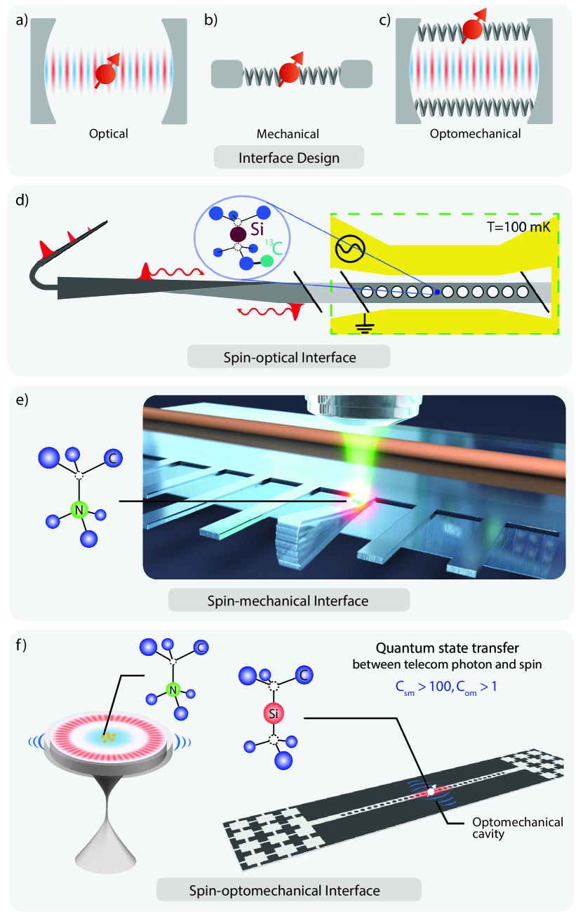
Coherent qubit-photon coupling is inherently limited by the weak light-matter interaction[19]. However, as depicted in Fig. 7 (a), cavity quantum electrodynamics (QED) provides a promising route to overcome this hurdle by strong confinement of light inside optical resonators, thus enhancing the qubit-photon interactions[398]. In principle, solid-state emitters embedded in nanophotonic cavity QED devices offer scalable fabrication[399], on-chip photonic routing[325], and electronic- and mechanical control[64, 400]: key requirements for integrated network nodes in large-scale quantum networks.
For quantum network applications, the spin-photon interface has to operate in a regime where a single photon coherently and reversibly couples to a spin qubit. In general, the coupling between two different quantum systems is characterized by the cooperativity parameter , defined as[19]
| (4) |
where is the coupling rate between the systems and are the energy decay rates of each system. The condition enables coherent interaction between the two quantum systems, despite their internal decoherence, and has been demonstrated for a variety of systems, including, but not limited to, atoms[401], superconducting resonators[402], molecules[403, 404], and semiconductor QDs[398]. However, the optical coherence of solid-state emitters is strongly influenced by the host material[405, 293]: interactions with the local environment leading to the inhomogeneous broadening of the optical linewidth and consequently loss of photon coherence. The effect of inhomogeneous broadening (with rate ) can be incorporated by introducing the coherence cooperativity[160, 293], where in Eq. 4[309].
Remote entanglement protocols relying on two-photon quantum interference require a high flux of coherent indistinguishable photons. In the Barrett and Kok protocol[407], successful entanglement events are heralded by the detection of two independent ZPL photons. The overall success rate of this protocol scales with , where is the probability of detecting a ZPL photon and the factor accounts for the need to detect two photons per successful entanglement event. As discussed in Section VI, can be drastically enhanced by utilizing the Purcell effect in cavity QED devices.
To date, all experiments demonstrating remote entanglement of color centers in diamond[46, 47] have been conducted using native NV centers and SILs[274]. Reversible spin-photon coupling requires , a condition that cannot be satisfied using SILs. In practice, NV centers embedded in cavities typically suffer from inhomogeneous linewidth broadening[123], manifested by compromised photon indistinguishability and . While recent results using native NV centers in nanopillars are promising[408], for network nodes using NV centers, the long-term optical stability remains a significant hurdle. On the other hand, nanoscale positioning of SiV centers in nanocavities, depicted schematically in Fig. 7 (d), shows remarkable properties; [43], enabling spin-state dependent photon reflection and single-shot spin-state readout with fidelity , combined with a fiber collection efficiency surpassing [190] have been demonstrated. However, at the time of writing, entanglement of remote SiV centers, or any other group-IV defects, remains to be reported.
VIII-A Strategies for a Universal Qubit–Photon Interface
It is likely that future long-distance quantum networks will make use of existing low-loss fiber infrastructure. However, to date, most cavity-spin systems operate at wavelengths resonant with the spin optical transition, usually in the visible range where fiber loss is high relative to telecommunication wavelengths. Coherent, entanglement preserving quantum frequency down-conversion from visible to telecommunication wavelengths is therefore required to minimize losses in the fiber links[72, 409, 410, 411]. However, cavity QED systems with subsequent frequency down-conversion, while promising, come with limitations. First and foremost, for this approach to work, the qubit system must exhibit well-defined intrinsic spin-conserving optical transitions, a feature absent for popular qubit platforms such as gate-defined quantum dots and superconducting resonators. Second, differences in the local environment leads to spectral wandering, rendering photon emission from two cavities distinguishable. At the time of writing, cavity-enhanced entanglement of remote color centers in diamond has yet to be demonstrated.
An active area of research to tackle these challenges at a fundamental level involves using mechanical systems. Mechanical degrees of freedom are central to many quantum technologies[412], thanks to their ability to couple to a wide range of fields–electrical, magnetic, optical, and gravitational–through device engineering[413]. Nanomechanical systems can be naturally integrated with solid-state quantum systems by on-chip fabrication, providing a universal platform to interface a variety of solid-state qubit systems. For example, phonons have been used to mediate quantum gates between trapped ions[414], coherently connect superconducting qubits[415] and to manipulate quantum-dot single-photon sources[416, 417]. The last decade has seen significant experimental effort towards coupling between spin qubits and mechanical motion[153].
Spins can be coupled to mechanics via induced strain in their host crystal or a oscillating magnetic moment [418], and can be modeled using the canonical system shown in Fig. 7 (b). In recent experiments, coupling between piezoelectronically actuated mechanical motion and electronic spins has been realized for color centers in bulk diamond and SiC[419, 420, 421, 422], in hybrid nanowire[423, 424] and cantilever mechanical resonators (see Fig. 7 (e))[425, 426, 427, 146]. However, combining these spin-mechanical devices with a coherent optical interface remains challenging owing to the weak interaction between photons and mechanical motion.
Cavity optomechanical devices provide a platform to enhance the spin-phonon-photon interaction by integrating mechanical resonators within optical cavities (See Sec. III). In a cavity optomechanical system, resonant optical recirculation extends the photon-phonon interaction time, and a parametric enhancement of the optomechanical coupling rate, , proportional to the intracavity photon number can be exploited. A cavity optomechanical device can be designed to support optical modes in the telecommunication wavelength range, while simultaneously supporting mechanical modes resonant with the qubit spin transitions. To maximize the spin-phonon and photon-phonon coupling rates, the devices can be engineered to minimize mechanical and optical mode volumes, respectively[426]. Nanoscale cavity optomechanical devices such as optomechanical crystals [428] and microdisks [76] typically support mechanical modes in the gigahertz frequency regime, which can be cooled to their quantum ground state [429, 211, 161] in a dilution fridge.
The operating principle of a spin-optomechanical interface based on spin-strain coupling is twofold, see Fig. 7 (c): radiation pressure from photons in an optical mode coherently excites the vibrations of a mechanical mode. This vibrational motion creates a microscopic stress field oscillating at the mechanical resonance frequency, which can interact with embedded spin qubits. The optomechanical interaction can be tuned for reversible photon-phonon conversion, and can operate at any wavelength resonant with a low-loss mode of the optical cavity. Recently, a proof-of-principle realization of a room-temperature cavity optomechanical spin-photon interface was demonstrated using a diamond microdisk resonator[74]. In this work, a photonic coherent state in the 1,550 nm telecommunication wavelength band was used to manipulate the electronic spin of a small ensemble of NV centers. Crucially, the resulting spin-photon interface does not rely on the intrinsic optical transitions of the color centers, thereby mitigating the aforementioned problems with spectral stability[74]. Moreover, this approach is completely generic, and can be applied to color centers in other host materials[430, 431, 432, 433, 434], alongside providing a method to control optically inactive qubits[435, 436].
VIII-B Universal Optomechanical Spin Interface: Challenges and Solutions
As previously discussed, quantum network applications require operation in a regime where a single photon coherently and reversibly couples to a spin qubit. In optomechanical devices, coherent spin-phonon interaction can be reached provided both the optomechanical- and the spin-phonon cooperativity and , respectively, exceed the thermal phonon number . Cooling of the mechanical resonator to near the mechanical ground state ensures – the following discussion will therefore ignore . Assuming both the photon-phonon and the spin-phonon couplings are always ‘on’, the transduction efficiency of such a two-interface system is given by [78]:
| (5) |
A near-unity transduction efficiency is achievable in the limit [78]. However, recent proposals lift the above restriction by employing temporal control of the coupling rates[81, 437].
The condition has routinely been demonstrated in diamond optomechanical devices (see Sec. III). However, an outstanding technical challenge is to perform coherent photon-phonon conversion in a device cryogenically cooled to near its mechanical quantum ground state, without heating due to optical absorption. Ground-state cooling, recently demonstrated in silicon optomechanical quantum memories[161, 162], will be aided by diamonds low nonlinear absorption and excellent thermal properties[166].
To date, realizing has been hindered by the intrinsically weak spin-phonon coupling for the NV center ground state[74]. However, in principle, reaching the coherent transduction regime is possible using already demonstrated diamond cavity optomechanical devices coupled to spin states with higher stress-sensitivity. For example, using SiV centers in microdisk resonators allows for , owing to their -fold enhanced sensitivity to strain compared to the NV center ground state[153]. Embedding SiV centers in optomechanical crystals will further increase on the account of smaller mechanical mode volume and a lower damping rate. Upon doing so, the regime can be reached using already demonstrated spin qubits and devices[77, 194, 387, 74]. Incorporating phononic shields can drastically reduce , potentially enabling , paving the way for deterministic quantum state transfer between single telecom photons and single spins[74] and the use of phonons as on-chip quantum information carriers[438, 439]. Working with SiV centers necessitates operation at mK temperatures. However, the NV center ground-state spins coupled via a phonon-assisted optical Raman process can reach similar high cooperativities at 8 K[420], albeit stabilizing the optical transition of NV centers in nanostructures presents a formidable challenge.
IX Outlook: Enabling Quantum Networks with Diamond Integrated Photonics
Developments in diamond photonics have advanced tremendously over the years. However, to realize a fully functional quantum network, and for related quantum technologies to reach their maximum potential, there are numerous obstacles to overcome. A roadmap highlighting imminent challenges and future objectives in relation to quantum hardware elements is presented in Fig. 8. The following discussion is centered around addressing these challenges within the context of integrated diamond photonics.
IX-A Robust Qubits
For quantum networking protocols using NV centers [47, 41, 48, 49], scalability is limited by the low flux of coherent photons. While, in principle, resonant coupling to a cavity enhances the photon flux[123], NV centers embedded in nanophotonic cavities typically suffer from inhomogeneous linewidth broadening[231], compromising photon indistinguishability and limiting the achievable entanglement rates, thus necessitating tuning and stabilizing of the ZPL transition[341, 440]. On the contrary, environment-insensitive color centers, such as SiV, perform excellently in nanophotonic resonators[43]. However, the SiV center experience heating-induced spin decoherence manifesting in slow and low-fidelity coherent microwave control[316, 130]. These limitations motivate the investigation of novel color centers.
As discussed briefly in Section II-A, careful control of defect concentration and boron doping, stabilizes the neutral SiV center, SiV0[119]. With a ground-state, SiV0 combines the excellent spin properties of the NV center ( at 4 K[119]) with the favourable optical properties of SiV-[441, 119]. Research on SiV0 is still in the early stages, largely limited by the Fermi level pinning required to stabilize the charge state[119].
| Color center | (nm) | Radiative lifetime (ns) | QE () | DW factor | (GHz) |
| SiV- | 7381 | 2 | 3 | 0.74 | 485 |
| SiV0 | 9466 | 7 | Not known | 0.98 | N /A |
| GeV- | 6029 | 10 | 12-2511 | 0.612 | 13 |
| SnV- | 62014 | 15 | 8014 | 0.5716 | 85014 |
| PbV- | 52017 / 55018 | 17,18 | Not known | Not known | 570017 / 400019 |
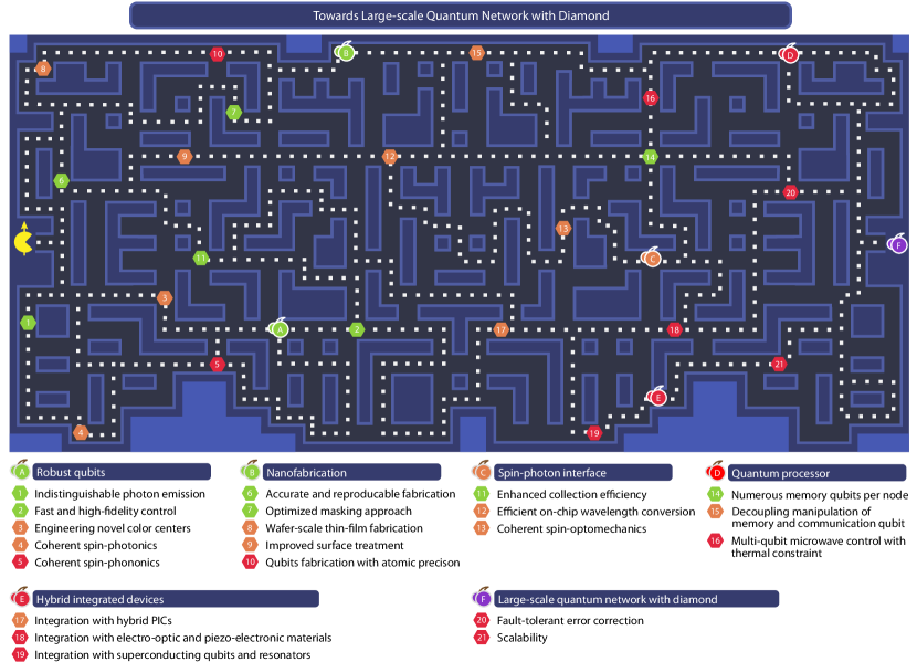
For the negatively charged group-IV color centers, the ground-state splitting is found to increase with atomic number, owing to stronger spin-orbit interactions[446]. As a consequence, phonon-assisted population transfer between the orbital ground-states is suppressed, leading to prolonged spin coherence times at elevated temperatures[443, 447, 112]. Table II summarizes and compares the key physical properties of group-IV color centers. Note that research on the PbV center is still in the early stages and key parameters remain to be determined with consistency[445].
Additionally, the reversible and coherent spin-photon coupling could, in principle, enable on-chip entanglement routing, thus potentially improving the communication rate[448]. Alternatively, coupling of spins to propagating phonons has been proposed as a means to implement scalable, high-fidelity and hybrid on-chip quantum networks[438, 439].
IX-B Nanofabrication
The performance of integrated quantum photonic systems relies fundamentally on the engineering and nanofabrication of their key components. Significant progress has been made in the nanostructuring of single-crystal diamond since the demonstration of nanowire antennas[299] and microring resonators[321, 231] over a decade ago to the recent realization of complex optomechanical devices integrated as spin-photon interfaces and waveguides in large-scale platforms[325]. The lack of wafer-scale single-crystal diamond, though, limits the scalability of integrated photonic architectures and is a significant impediment to the realization of scalable fabrication analogous to what is achieved in the semiconductor industry.
A key challenge in diamond nanostructuring is the mitigation of surface roughness that arises from the transfer of lithographically defined mask edge defects and mask erosion during plasma etching, as well as imperfections inherent to the diamond surface which have evolved from inhomogeneities on the seed substrate during CVD growth[449]. This roughness can lead to degradation of both optical and acoustic (both bulk- and phononic-mode) quality factors, affecting the coupling between the two systems and hindering the transmission of information over long distances required for quantum communications applications. The fabrication of devices with dimensions required for smaller optical mode volumes is also affected by the prevalence of defects. Efforts for surface roughness abatement prior to nanofabrication processes have included fine mechanical, chemical, and plasma-based smoothing[450], though the mechanisms for the anisotropic wear along different crystal facets during polishing are not yet well understood and therefore results can vary significantly based on methods[451]. There is also a necessity for the development of more robust, higher resolution electron beam resists with improved adhesion, as well as the optimization of hard masks and diamond plasma etching conditions.
The creation of color centers with long coherence times at the surface or subsurface (within a few tens of nanometers) of diamond devices is an ongoing endeavor. Lattice defects induced by ion implantation as well as those inherent at the diamond surface create charge potentials that couple to the dipole moment of the spin[452], leading to dephasing between the two charge states and resulting in optical linewidth broadening compared to what is exhibited in the bulk[90, 334]. Several approaches have been made to understand and lessen the impacts of ion implantation, such as exposure through lithographically defined masks to minimize scattering[453] and post dosage annealing, though these methods have not been perfected. Surface and subsurface damage removal has been accomplished through oxygen termination of the diamond surface post-annealing, improving optical linewidths and spin coherence by an order of magnitude[450].
IX-C Spin-Photon Interface
The realization of a quantum network hinges on the interconnection of remote network nodes[6]. Cavity QED devices offer an ideal platform to interface stationary spin qubits with photons on account of the enhanced light-matter interactions[19]. These devices need to combine a large photon extraction efficiency[43] with the capability of tuning the emission frequency via on-chip application of electrical[46] or mechanical[454, 400] fields and microwaves for spin control. In addition, efficient on-chip frequency down-conversion from visible to telecommunication band is required to mitigate losses in the photonic links. Heralded entanglement schemes rely on quantum interference of indistinguishable photons. Quantum frequency down-conversion provides a method for interfering photons from spectrally distinguishable emitters, by detuning the pump laser to compensate for the spectral difference[455]. Alternatively, coherent photon-phonon and spin-phonon coupling in an optomechanical cavity provide a way to realize a spin-photon interface operating directly at telecom wavelengths[74, 418, 83].
IX-D Quantum Processor
A universal quantum processor consists of numerous qubits with long coherence times while supporting conditional and unconditional quantum gates[84]. The realization of such a multi-qubit processor requires quantum gates to individually address the memory qubits, without introducing cross-talk affecting the coherence of the remaining spin-register[98]. Using dynamical-decoupling sequences[456, 457, 111, 458] and selective coupling to 13C nuclear spins, a ten-qubit spin register based on the NV center has successfully been demonstrated[98]. While coupling to 13C nuclear spins has been demonstrated for the SiV center[316, 43], extending these results to multi-qubit registers remains challenging, owing to the spin-half nature of both the SiV and C spin systems that requires extended decoupling times[293, 316]. Realizing a multi-qubit register based on SiV or other group-IV color centers requires experimental effort to mitigate the aforementioned problem with heating-induced spin decoherence as a result of the applied microwave pulses.
IX-E Hybrid Integrated Devices
Hybrid integrated devices combine the strengths of disparate quantum systems to build complex quantum architectures. While individual monolithic diamond spin-photon interfaces have been realized with excellent performance[190], wafer-scale device fabrication remains elusive[325]. Interfacing diamond with well-established photonic materials, such as AlN and GaP, provides a path towards incorporating diamond in photonic integrated circuits (PIC) for on-chip photon routing[325]. Furthermore, using materials with strong -nonlinearities enables on-chip frequency conversion[459, 460]. In addition, frequency shifting of single photons using electro-optical modulators paves the way for the entanglement of spectrally distinguishable quantum emitters[461].
Finally, piezo-electric materials have been proposed as a phononic interface between superconducting qubits and quantum memories based on color centers in diamond[437]. In this transduction scheme, a microwave photon is converted to a phonon via the piezoelectric effect, which further interacts with the quantum memory via spin-phonon coupling[462]. Quantum interference of the emitted photons thus enables entanglement of remote superconducting circuits. An advantage of this quantum memory-based transduction scheme over direct microwave-to-optical-photon conversion is a potential reduction in heating of the cryostat on account of the lower laser power required, which might preserve the coherence of the superconducting resonators[462].
IX-F Error Correction and Scalability
Quantum systems are inherently noisy: interactions with the environment lead to decoherence, inevitably manifested by the emergence of errors[109]. Correcting errors is therefore a necessity. Quantum error correction protocols have been demonstrated on spin registers based on NV centers in diamond[84, 109, 110, 463]. These protocols harness the weak coupling between the electron spin and the surrounding nuclear spins. Recently, this development was pushed one step further by the demonstration of fault-tolerant operations on a diamond quantum processor[37]. While in the early stages, the successful implementation of fault-tolerant operations has the potential to bring diamond to the forefront of quantum information processing based on solid-state spins.
At the time of writing, the scalability of diamond as a platform for quantum information processing is limited in part by challenges in nanofabrication and large-scale growth of single-crystal diamond[464]. A tremendous experimental effort is being invested to advance the state-of-the-art in diamond fabrication[200, 465], and the aforementioned hybrid platforms provide a promising route to realize scalable photonic platforms [325]. In parallel, new techniques[466] are being pursued to increase the quality[467] and size[468, 234] of synthetic diamonds. However, despite this progress large-scale synthetic growth of single-crystal diamond wafers remains elusive.
Concluding Remarks
Research in the field of diamond integrated quantum photonics is vibrant and fast-moving, owing to diamond’s unique combination of physical properties and ability to host robust spin qubits. In this article, we have reviewed the current state-of-the-art in the field, with particular emphasis on advances and outstanding challenges in nanofabrication, cavity optomechanics, and the development of qubit-photon interfaces. To conclude, we provided a road map illuminating the path towards the realization of a universal quantum network.
References
- [1]
- [2] W. Gerlach and O. Stern, “Der experimentelle nachweis der richtungsquantelung im magnetfeld,” Zeitschrift fur Physik, vol. 9, pp. 349–352, 12 1922. [Online]. Available: http://doi.org/10.1007/BF01326983
- [3] D. P. DiVincenzo, “Quantum computation,” Science, vol. 270, pp. 255–261, 10 1995. [Online]. Available: https://doi.org/10.1126/science.270.5234.255
- [4] T. D. Ladd, F. Jelezko, R. Laflamme, Y. Nakamura, C. Monroe, and J. L. O’Brien, “Quantum computers,” Nature, vol. 464, no. 7285, pp. 45–53, mar 2010. [Online]. Available: http://doi.org/10.1038/nature08812
- [5] N. Gisin and R. Thew, “Quantum communication,” Nature Photonics, vol. 1, pp. 165–171, 3 2007. [Online]. Available: http://doi.org/10.1038/nphoton.2007.22
- [6] H. J. Kimble, “The quantum internet,” Nature, vol. 453, no. 7198, pp. 1023–1030, jun 2008. [Online]. Available: http://doi.org/10.1038/nature07127
- [7] V. Giovannetti, S. Lloyd, and L. Maccone, “Quantum-enhanced measurements: Beating the standard quantum limit,” Science, vol. 306, pp. 1330–1336, 11 2004. [Online]. Available: https://doi.org/10.1126/science.1104149
- [8] S. L. Vittorio Giovannetti and L. Maccone, “Quantum metrology,” Physical Review Letters, vol. 96, p. 010401, 1 2006. [Online]. Available: https://doi.org/10.1103/PhysRevLett.96.010401
- [9] C. L. Degen, F. Reinhard, and P. Cappellaro, “Quantum sensing,” Reviews of Modern Physics, vol. 89, no. 3, p. 35002, jul 2017. [Online]. Available: https://doi.org/10.1103/RevModPhys.89.035002
- [10] F. Arute et al., “Quantum supremacy using a programmable superconducting processor,” Nature, vol. 574, pp. 505–510, 10 2019. [Online]. Available: http://doi.org/10.1038/s41586-019-1666-5
- [11] H.-S. Zhong et al., “Quantum computational advantage using photons,” Science, vol. 370, pp. 1460–1463, 12 2020. [Online]. Available: https://doi.org/10.1126/science.abe8770
- [12] Y. Wu et al., “Strong quantum computational advantage using a superconducting quantum processor,” Physical Review Letters, vol. 127, p. 180501, 10 2021. [Online]. Available: https://doi.org/10.1103/PhysRevLett.127.180501
- [13] L. S. Madsen et al., “Quantum computational advantage with a programmable photonic processor,” Nature, vol. 606, pp. 75–81, 6 2022. [Online]. Available: https://doi.org/10.1038/s41586-022-04725-x
- [14] S.-K. Liao et al., “Satellite-relayed intercontinental quantum network,” Physical Review Letters, vol. 120, p. 030501, 1 2018. [Online]. Available: https://link.aps.org/doi/10.1103/PhysRevLett.120.030501
- [15] J. Yin et al., “Entanglement-based secure quantum cryptography over 1,120 kilometres,” Nature, vol. 582, no. 7813, pp. 501–505, 2020. [Online]. Available: https://doi.org/10.1038/s41586-020-2401-y
- [16] P. H. Kim, B. D. Hauer, C. Doolin, F. Souris, and J. P. Davis, “Approaching the standard quantum limit of mechanical torque sensing,” Nature Communications, vol. 7, p. 13165, 12 2016. [Online]. Available: http://doi.org/10.1038/ncomms13165
- [17] L.-M. Duan and C. Monroe, “Colloquium : Quantum networks with trapped ions,” Reviews of Modern Physics, vol. 82, pp. 1209–1224, 4 2010. [Online]. Available: https://doi.org/10.1103/RevModPhys.82.1209
- [18] S. Ritter et al., “An elementary quantum network of single atoms in optical cavities,” Nature, vol. 484, no. 7393, pp. 195–200, apr 2012. [Online]. Available: http://doi.org/10.1038/nature11023
- [19] A. Reiserer and G. Rempe, “Cavity-based quantum networks with single atoms and optical photons,” Reviews of Modern Physics, vol. 87, pp. 1379–1418, 12 2015. [Online]. Available: https://doi.org/10.1103/RevModPhys.87.1379
- [20] O. Hosten, N. J. Engelsen, R. Krishnakumar, and M. A. Kasevich, “Measurement noise 100 times lower than the quantum-projection limit using entangled atoms,” Nature, vol. 529, pp. 505–508, 1 2016. [Online]. Available: http://doi.org/10.1038/nature16176
- [21] L. Stephenson et al., “High-rate, high-fidelity entanglement of qubits across an elementary quantum network,” Physical Review Letters, vol. 124, p. 110501, 3 2020. [Online]. Available: https://doi.org/10.1103/PhysRevLett.124.110501
- [22] L. Egan et al., “Fault-tolerant control of an error-corrected qubit,” Nature, vol. 598, pp. 281–286, 10 2021. [Online]. Available: https://doi.org/10.1038/s41586-021-03928-y
- [23] S. Langenfeld, P. Thomas, O. Morin, and G. Rempe, “Quantum repeater node demonstrating unconditionally secure key distribution,” Physical Review Letters, vol. 126, p. 230506, 6 2021. [Online]. Available: https://doi.org/10.1103/PhysRevLett.126.230506
- [24] S. Langenfeld et al., “Quantum teleportation between remote qubit memories with only a single photon as a resource,” Physical Review Letters, vol. 126, p. 130502, 3 2021. [Online]. Available: https://doi.org/10.1103/PhysRevLett.126.130502
- [25] T. van Leent et al., “Entangling single atoms over 33 km telecom fibre,” Nature, vol. 607, no. 7917, pp. 69–73, 2022. [Online]. Available: https://doi.org/10.1038/s41586-022-04764-4
- [26] W. F. Koehl, H. Seo, G. Galli, and D. D. Awschalom, “Designing defect spins for wafer-scale quantum technologies,” MRS Bulletin, vol. 40, pp. 1146–1153, 12 2015. [Online]. Available: http://doi.org/10.1557/mrs.2015.266
- [27] M. H. Devoret and R. J. Schoelkopf, “Superconducting circuits for quantum information: An outlook,” Science, vol. 339, pp. 1169–1174, 3 2013. [Online]. Available: https://doi.org/10.1126/science.1231930
- [28] R. Hanson, L. P. Kouwenhoven, J. R. Petta, S. Tarucha, and L. M. K. Vandersypen, “Spins in few-electron quantum dots,” Reviews of Modern Physics, vol. 79, pp. 1217–1265, 10 2007. [Online]. Available: https://doi.org/10.1103/RevModPhys.79.1217
- [29] G. Burkard, T. D. Ladd, J. M. Nichol, A. Pan, and J. R. Petta, “Semiconductor spin qubits,” arXiv preprint arXiv:2112.08863, 2021. [Online]. Available: https://doi.org/10.48550/arXiv.2112.08863
- [30] D. D. Awschalom, R. Hanson, J. Wrachtrup, and B. B. Zhou, “Quantum technologies with optically interfaced solid-state spins,” Nature Photonics, vol. 12, no. 9, pp. 516–527, sep 2018. [Online]. Available: http://doi.org/10.1038/s41566-018-0232-2
- [31] J. L. O’Brien, A. Furusawa, and J. Vučković, “Photonic quantum technologies,” Nature Photonics, vol. 3, pp. 687–695, 12 2009. [Online]. Available: http://doi.org/10.1038/nphoton.2009.229
- [32] P. Kómár et al., “A quantum network of clocks,” Nature Physics, vol. 10, no. 8, pp. 582–587, aug 2014. [Online]. Available: http://doi.org/10.1038/nphys3000
- [33] A. K. Ekert, “Quantum cryptography based on bell’s theorem,” Physical Review Letters, vol. 67, pp. 661–663, 8 1991. [Online]. Available: https://doi.org/10.1103/PhysRevLett.67.661
- [34] N. Gisin, G. Ribordy, W. Tittel, and H. Zbinden, “Quantum cryptography,” Reviews of Modern Physics, vol. 74, no. 1, pp. 145–195, mar 2002. [Online]. Available: https://doi.org/10.1103/RevModPhys.74.145
- [35] T. E. Northup and R. Blatt, “Quantum information transfer using photons,” Nature Photonics, vol. 8, pp. 356–363, 5 2014. [Online]. Available: http://doi.org/10.1038/nphoton.2014.53
- [36] S. Wehner, D. Elkouss, and R. Hanson, “Quantum internet: A vision for the road ahead,” Science, vol. 362, no. 6412, oct 2018. [Online]. Available: http://doi.org/10.1126/science.aam9288
- [37] M. H. Abobeih et al., “Fault-tolerant operation of a logical qubit in a diamond quantum processor,” Nature, 5 2022. [Online]. Available: https://doi.org/10.1038/s41586-022-04819-6
- [38] R. Valivarthi et al., “Quantum teleportation across a metropolitan fibre network,” Nature Photonics, vol. 10, pp. 676–680, 10 2016. [Online]. Available: http://doi.org/10.1038/nphoton.2016.180
- [39] M. E. Wandel, “Attenuation in silica-based optical fibers,” 2006. [Online]. Available: https://orbit.dtu.dk/en/publications/attenuation-in-silica-based-optical-fibers
- [40] W. Pfaff et al., “Unconditional quantum teleportation between distant solid-state quantum bits,” Science, vol. 345, no. 6196, pp. 532–535, 2014. [Online]. Available: https://doi.org/10.1126/science.1253512
- [41] N. Kalb et al., “Entanglement distillation between solid-state quantum network nodes,” Science, vol. 356, no. 6341, pp. 928–932, jun 2017. [Online]. Available: http://doi.org/10.1126/science.aan0070
- [42] R. E. Evans et al., “Photon-mediated interactions between quantum emitters in a diamond nanocavity,” Science, vol. 362, pp. 662–665, 11 2018. [Online]. Available: https://doi.org/10.1126/science.aau4691
- [43] M. K. Bhaskar et al., “Experimental demonstration of memory-enhanced quantum communication,” Nature, pp. 1–5, mar 2020. [Online]. Available: http://doi.org/10.1038/s41586-020-2103-5
- [44] M. Pompili et al., “Experimental demonstration of entanglement delivery using a quantum network stack,” 11 2021. [Online]. Available: https://doi.org/10.48550/arXiv.2111.11332
- [45] E. Togan et al., “Quantum entanglement between an optical photon and a solid-state spin qubit.” Nature, vol. 466, no. 7307, pp. 730–4, aug 2010. [Online]. Available: http://doi.org/10.1038/nature09256
- [46] H. Bernien et al., “Heralded entanglement between solid-state qubits separated by three metres,” Nature, vol. 497, pp. 86–90, 5 2013. [Online]. Available: http://doi.org/10.1038/nature12016
- [47] B. Hensen et al., “Loophole-free Bell inequality violation using electron spins separated by 1.3 kilometres,” Nature, vol. 526, no. 7575, pp. 682–686, oct 2015. [Online]. Available: http://doi.org/10.1038/nature15759
- [48] P. C. Humphreys et al., “Deterministic delivery of remote entanglement on a quantum network,” Nature, vol. 558, no. 7709, pp. 268–273, jun 2018. [Online]. Available: http://doi.org/10.1038/s41586-018-0200-5
- [49] M. Pompili et al., “Realization of a multinode quantum network of remote solid-state qubits,” Science, vol. 372, no. 6539, pp. 259–264, 2021. [Online]. Available: http://doi.org/10.1126/science.abg1919
- [50] S. L. N. Hermans, M. Pompili, H. K. C. Beukers, S. Baier, J. Borregaard, and R. Hanson, “Qubit teleportation between non-neighbouring nodes in a quantum network,” Nature, vol. 605, pp. 663–668, 5 2022. [Online]. Available: https://doi.org/10.1038/s41586-022-04697-y
- [51] J. Hofmann et al., “Heralded entanglement between widely separated atoms,” Science, vol. 336, no. 6090, pp. 72–75, jul 2012. [Online]. Available: https://doi.org/10.1126/science.1221856
- [52] S. Daiss et al., “A quantum-logic gate between distant quantum-network modules,” Science, vol. 371, no. 6529, pp. 614–617, 2021. [Online]. Available: https://doi.org/10.1126/science.abe3150
- [53] D. L. Moehring et al., “Entanglement of single-atom quantum bits at a distance,” Nature, vol. 449, no. 7158, pp. 68–71, sep 2007. [Online]. Available: http://doi.org/10.1038/nature06118
- [54] D. Bluvstein et al., “A quantum processor based on coherent transport of entangled atom arrays,” Nature, vol. 604, pp. 451–456, 4 2022. [Online]. Available: https://doi.org/10.1038/s41586-022-04592-6
- [55] T. M. Graham et al., “Multi-qubit entanglement and algorithms on a neutral-atom quantum computer,” Nature, vol. 604, pp. 457–462, 4 2022. [Online]. Available: https://doi.org/10.1038/s41586-022-04603-6
- [56] A. Blais, S. M. Girvin, and W. D. Oliver, “Quantum information processing and quantum optics with circuit quantum electrodynamics,” Nature Physics, vol. 16, no. 3, pp. 247–256, mar 2020. [Online]. Available: http://doi.org/10.1038/s41567-020-0806-z
- [57] S. Krinner et al., “Realizing repeated quantum error correction in a distance-three surface code,” Nature, vol. 605, no. 7911, pp. 669–674, may 2022. [Online]. Available: http://doi.org/10.1038/s41586-022-04566-8
- [58] R. J. Warburton, “Single spins in self-assembled quantum dots,” Nature materials, vol. 12, no. 6, pp. 483–493, 2013. [Online]. Available: https://doi.org/10.1038/nmat3585
- [59] R. Stockill et al., “Phase-Tuned Entangled State Generation between Distant Spin Qubits,” Physical Review Letters, vol. 119, p. 010503, 7 2017. [Online]. Available: http://doi.org/10.1103/PhysRevLett.119.010503
- [60] L. Zhai et al., “Quantum interference of identical photons from remote gaas quantum dots,” Nature Nanotechnology, 5 2022. [Online]. Available: https://doi.org/10.1038/s41565-022-01131-2
- [61] M. Zhong et al., “Optically addressable nuclear spins in a solid with a six-hour coherence time,” Nature, vol. 517, no. 7533, pp. 177–180, jan 2015. [Online]. Available: http://doi.org/10.1038/nature14025
- [62] T. Zhong et al., “Nanophotonic rare-earth quantum memory with optically controlled retrieval,” Science, vol. 357, no. 6358, pp. 1392–1395, sep 2017. [Online]. Available: https://doi.org/10.1126/science.aan5959
- [63] A. M. Dibos, M. Raha, C. M. Phenicie, and J. D. Thompson, “Atomic Source of Single Photons in the Telecom Band,” Physical Review Letters, vol. 120, no. 24, p. 243601, jun 2018. [Online]. Available: https://doi.org/10.1103/PhysRevLett.120.243601
- [64] C. P. Anderson et al., “Electrical and optical control of single spins integrated in scalable semiconductor devices,” Science, vol. 366, pp. 1225–1230, 12 2019. [Online]. Available: https://doi.org/doi/10.1126/science.aax9406
- [65] J. M. Kindem, A. Ruskuc, J. G. Bartholomew, J. Rochman, Y. Q. Huan, and A. Faraon, “Control and single-shot readout of an ion embedded in a nanophotonic cavity,” Nature, pp. 1–4, mar 2020. [Online]. Available: http://doi.org/10.1038/s41586-020-2160-9
- [66] D. M. Lukin, M. A. Guidry, and J. Vučković, “Integrated quantum photonics with silicon carbide: Challenges and prospects,” PRX Quantum, vol. 1, p. 020102, 12 2020. [Online]. Available: http://doi.org/10.1103/PRXQuantum.1.020102
- [67] N. T. Son et al., “Developing silicon carbide for quantum spintronics,” Applied Physics Letters, vol. 116, p. 190501, 5 2020. [Online]. Available: http://doi.org/10.1063/5.0004454
- [68] A. Bourassa et al., “Entanglement and control of single nuclear spins in isotopically engineered silicon carbide,” Nature Materials, vol. 19, no. 12, pp. 1319–1325, dec 2020. [Online]. Available: https://doi.org/10.1038/s41563-020-00802-6
- [69] G. Wolfowicz, C. P. Anderson, B. Diler, O. G. Poluektov, F. J. Heremans, and D. D. Awschalom, “Vanadium spin qubits as telecom quantum emitters in silicon carbide,” Science Advances, vol. 6, no. 18, pp. 2–10, may 2020. [Online]. Available: https://doi.org/10.1126/sciadv.aaz1192
- [70] C. Babin et al., “Fabrication and nanophotonic waveguide integration of silicon carbide colour centres with preserved spin-optical coherence,” Nature Materials, vol. 21, no. 1, pp. 67–73, jan 2022. [Online]. Available: https://doi.org/10.1038/s41563-021-01148-3
- [71] D. M. Lukin et al., “Optical superradiance of a pair of color centers in an integrated silicon-carbide-on-insulator microresonator,” 2 2022. [Online]. Available: https://doi.org/10.48550/arXiv.2202.04845
- [72] A. Dréau, A. Tcheborateva, A. E. Mahdaoui, C. Bonato, and R. Hanson, “Quantum Frequency Conversion of Single Photons from a Nitrogen-Vacancy Center in Diamond to Telecommunication Wavelengths,” Physical Review Applied, vol. 9, no. 6, p. 064031, jun 2018. [Online]. Available: https://doi.org/10.1103/PhysRevApplied.9.064031
- [73] C. A. Regal and K. W. Lehnert, “From cavity electromechanics to cavity optomechanics,” Journal of Physics: Conference Series, vol. 264, p. 12025, 2011. [Online]. Available: https://doi.org/10.1088/1742-6596/264/1/012025
- [74] P. K. Shandilya, D. P. Lake, M. J. Mitchell, D. D. Sukachev, and P. E. Barclay, “Optomechanical interface between telecom photons and spin quantum memory,” Nature Physics, vol. 17, pp. 1420–1425, 12 2021. [Online]. Available: https://doi.org/10.1038/s41567-021-01364-3
- [75] D. Lee, K. W. Lee, J. V. Cady, P. Ovartchaiyapong, and A. C. B. Jayich, “Topical review: spins and mechanics in diamond,” Journal of Optics, vol. 19, no. 3, p. 33001, 2017. [Online]. Available: https://doi.org/10.1088/2040-8986/aa52cd
- [76] M. Mitchell, B. Khanaliloo, D. P. Lake, T. Masuda, J. P. Hadden, and P. E. Barclay, “Single-crystal diamond low-dissipation cavity optomechanics,” Optica, vol. 3, no. 9, pp. 963–970, 2016. [Online]. Available: http://doi.org/10.1364/OPTICA.3.000963
- [77] M. J. Burek et al., “Diamond optomechanical crystals,” Optica, vol. 3, no. 12, pp. 1404–1411, 2016. [Online]. Available: http://doi.org/10.1364/OPTICA.3.001404
- [78] N. Lauk et al., “Perspectives on quantum transduction,” Quantum Science and Technology, vol. 5, no. 2, p. 20501, mar 2020. [Online]. Available: http://doi.org/10.1088/2058-9565/ab788a
- [79] Y. Chu and S. Gröblacher, “A perspective on hybrid quantum opto- and electromechanical systems,” Applied Physics Letters, vol. 117, p. 150503, 10 2020. [Online]. Available: http://doi.org/10.1063/5.0021088
- [80] L. Fan et al., “Superconducting cavity electro-optics: A platform for coherent photon conversion between superconducting and photonic circuits,” Science Advances, vol. 4, p. eaar4994, 8 2018. [Online]. Available: https://doi.org/10.1126/sciadv.aar4994
- [81] M. Mirhosseini, A. Sipahigil, M. Kalaee, and O. Painter, “Superconducting qubit to optical photon transduction,” Nature, vol. 588, pp. 599–603, 12 2020. [Online]. Available: http://doi.org/10.1038/s41586-020-3038-6
- [82] K. Stannigel, P. Rabl, A. S. Sørensen, P. Zoller, and M. D. Lukin, “Optomechanical transducers for long-distance quantum communication,” Physical Review Letters, vol. 105, p. 220501, 11 2010. [Online]. Available: https://doi.org/10.1103/PhysRevLett.105.220501
- [83] H. Raniwala, S. Krastanov, M. Eichenfield, and D. Englund, “A spin-optomechanical quantum interface enabled by an ultrasmall mechanical and optical mode volume cavity,” 2 2022. [Online]. Available: https://doi.org/10.48550/arXiv.2202.06999
- [84] T. H. Taminiau, J. Cramer, T. van der Sar, V. V. Dobrovitski, and R. Hanson, “Universal control and error correction in multi-qubit spin registers in diamond,” Nature Nanotechnology, vol. 9, pp. 171–176, 3 2014. [Online]. Available: http://doi.org/10.1038/nnano.2014.2
- [85] X. Rong et al., “Experimental fault-tolerant universal quantum gates with solid-state spins under ambient conditions,” Nature Communications, vol. 6, p. 8748, 12 2015. [Online]. Available: http://doi.org/10.1038/ncomms9748
- [86] Y. Chen, S. Stearn, S. Vella, A. Horsley, and M. W. Doherty, “Optimisation of diamond quantum processors,” New Journal of Physics, vol. 22, p. 093068, 9 2020. [Online]. Available: https://doi.org/10.1088/1367-2630/abb0fb
- [87] I. Bayn et al., “Generation of ensembles of individually resolvable nitrogen vacancies using nanometer-scale apertures in ultrahigh-aspect ratio planar implantation masks,” Nano Letters, vol. 15, pp. 1751–1758, 3 2015. [Online]. Available: https://doi.org/10.1021/nl504441m
- [88] M. Fuechsle et al., “A single-atom transistor,” Nature Nanotechnology, vol. 7, pp. 242–246, 4 2012. [Online]. Available: http://doi.org/10.1038/nnano.2012.21
- [89] S. C. Benjamin, B. W. Lovett, and J. M. Smith, “Prospects for measurement-based quantum computing with solid state spins,” Laser Photonics Rev., vol. 3, p. 556, 2009.
- [90] S. Chakravarthi, C. Pederson, Z. Kazi, A. Ivanov, and K.-M. C. Fu, “Impact of surface and laser-induced noise on the spectral stability of implanted nitrogen-vacancy centers in diamond,” Phys. Rev. B, vol. 104, p. 085425, Aug 2021. [Online]. Available: https://doi.org/10.1103/PhysRevB.104.085425
- [91] A. Zaitsev, Optical properties of diamond. Berlin, Heidelberg: Springer-Verlag Berlin Heidelberg, 2001. [Online]. Available: https://doi.org/10.1007/978-3-662-04548-0
- [92] I. Aharonovich, S. Castelletto, D. A. Simpson, C.-H. Su, A. D. Greentree, and S. Prawer, “Diamond-based single-photon emitters,” Reports on Progress in Physics, vol. 74, p. 076501, 7 2011. [Online]. Available: https://doi.org/10.1088/0034-4885/74/7/076501
- [93] L. Childress, R. Walsworth, and M. Lukin, “Atom-like crystal defects: From quantum computers to biological sensors,” Physics Today, vol. 67, pp. 38–43, 10 2014. [Online]. Available: http://doi.org/10.1063/PT.3.2549
- [94] T. Tohei, A. Kuwabara, F. Oba, and I. Tanaka, “Debye temperature and stiffness of carbon and boron nitride polymorphs from first principles calculations,” Physical Review B, vol. 73, p. 064304, 2 2006. [Online]. Available: https://doi.org/10.1103/PhysRevB.73.064304
- [95] G. Balasubramanian et al., “Ultralong spin coherence time in isotopically engineered diamond,” Nature Materials, vol. 8, no. 5, pp. 383–387, may 2009. [Online]. Available: http://doi.org/10.1038/nmat2420
- [96] L. Childress et al., “Coherent dynamics of coupled electron and nuclear spin qubits in diamond,” Science, vol. 314, pp. 281–285, 10 2006. [Online]. Available: https://doi.org/10.1126/science.1131871
- [97] P. C. Maurer et al., “Room-Temperature Quantum Bit Memory Exceeding One Second,” Science, vol. 336, no. 6086, pp. 1283–1286, 2012. [Online]. Available: http://doi.org/10.1126/science.1220513
- [98] C. E. Bradley et al., “A ten-qubit solid-state spin register with quantum memory up to one minute,” Physical Review X, vol. 9, p. 031045, 9 2019. [Online]. Available: https://doi.org/10.1103/PhysRevX.9.031045
- [99] F. Dolde et al., “Room-temperature entanglement between single defect spins in diamond,” Nature Physics, vol. 9, no. 3, pp. 139–143, mar 2013. [Online]. Available: http://doi.org/10.1038/nphys2545
- [100] M. V. G. Dutt et al., “Quantum register based on individual electronic and nuclear spin qubits in diamond.” Science (New York, N.Y.), vol. 316, no. 5829, pp. 1312–6, jun 2007. [Online]. Available: http://www.doi.org/10.1126/science.1139831
- [101] G. D. Fuchs, G. Burkard, P. V. Klimov, and D. D. Awschalom, “A quantum memory intrinsic to single nitrogen–vacancy centres in diamond,” Nature Physics, vol. 7, pp. 789–793, 10 2011. [Online]. Available: http://doi.org/10.1038/nphys2026
- [102] D. M. Toyli, C. D. Weis, G. D. Fuchs, T. Schenkel, and D. D. Awschalom, “Chip-scale nanofabrication of single spins and spin arrays in diamond,” Nano Letters, vol. 10, pp. 3168–3172, 8 2010. [Online]. Available: https://doi.org/10.1021/nl102066q
- [103] P. R. Dolan et al., “Robust, tunable, and high purity triggered single photon source at room temperature using a nitrogen-vacancy defect in diamond in an open microcavity,” Optics Express, vol. 26, p. 7056, 3 2018. [Online]. Available: https://doi.org/10.1364/OE.26.007056
- [104] E. N. Knall et al., “Efficient source of shaped single photons based on an integrated diamond nanophotonic system,” 1 2022. [Online]. Available: https://doi.org/10.48550/arXiv.2201.02731
- [105] M. W. Doherty, N. B. Manson, P. Delaney, F. Jelezko, J. Wrachtrup, and L. C. Hollenberg, “The nitrogen-vacancy colour centre in diamond,” Physics Reports, vol. 528, pp. 1–45, 7 2013. [Online]. Available: http://doi.org/10.1016/j.physrep.2013.02.001
- [106] J. N. Becker and E. Neu, “The silicon vacancy center in diamond,” pp. 201–235, 2020. [Online]. Available: https://doi.org/10.1016/bs.semsem.2020.04.001
- [107] S. Johnson, P. R. Dolan, and J. M. Smith, “Diamond photonics for distributed quantum networks,” Progress in Quantum Electronics, vol. 55, pp. 129–165, 9 2017. [Online]. Available: https://doi.org/10.1016/j.pquantelec.2017.05.003
- [108] L. Rondin, J.-P. Tetienne, T. Hingant, J.-F. Roch, P. Maletinsky, and V. Jacques, “Magnetometry with nitrogen-vacancy defects in diamond,” Reports on Progress in Physics, vol. 77, p. 056503, 5 2014. [Online]. Available: https://doi.org/10.1088/0034-4885/77/5/056503
- [109] G. Waldherr et al., “Quantum error correction in a solid-state hybrid spin register,” Nature, vol. 506, pp. 204–207, 2 2014. [Online]. Available: http://doi.org/10.1038/nature12919
- [110] J. Cramer et al., “Repeated quantum error correction on a continuously encoded qubit by real-time feedback,” Nature Communications, vol. 7, p. 11526, 9 2016. [Online]. Available: http://doi.org/10.1038/ncomms11526
- [111] M. H. Abobeih et al., “One-second coherence for a single electron spin coupled to a multi-qubit nuclear-spin environment,” Nature Communications, vol. 9, p. 2552, 12 2018. [Online]. Available: http://doi.org/10.1038/s41467-018-04916-z
- [112] C. Bradac, W. Gao, J. Forneris, M. E. Trusheim, and I. Aharonovich, “Quantum nanophotonics with group iv defects in diamond,” Nature Communications, vol. 10, p. 5625, 12 2019. [Online]. Available: http://doi.org/10.1038/s41467-019-13332-w
- [113] A. Gali and J. R. Maze, “Ab initio study of the split silicon-vacancy defect in diamond: Electronic structure and related properties,” Physical Review B, vol. 88, p. 235205, 12 2013. [Online]. Available: https://doi.org/10.1103/PhysRevB.88.235205
- [114] U. Wahl et al., “Direct structural identification and quantification of the split-vacancy configuration for implanted sn in diamond,” Physical Review Letters, vol. 125, p. 045301, 7 2020. [Online]. Available: https://doi.org/10.1103/PhysRevLett.125.045301
- [115] S. Aghaeimeibodi, D. Riedel, A. E. Rugar, C. Dory, and J. Vučković, “Electrical tuning of tin-vacancy centers in diamond,” Physical Review Applied, vol. 15, p. 064010, 6 2021. [Online]. Available: http://doi.org/10.1103/PhysRevApplied.15.064010
- [116] L. D. Santis, M. E. Trusheim, K. C. Chen, and D. R. Englund, “Investigation of the stark effect on a centrosymmetric quantum emitter in diamond,” Physical Review Letters, vol. 127, p. 147402, 9 2021. [Online]. Available: https://doi.org/10.1103/PhysRevLett.127.147402
- [117] N. B. Manson, J. P. Harrison, and M. J. Sellars, “Nitrogen-vacancy center in diamond: Model of the electronic structure and associated dynamics,” Physical Review B, vol. 74, p. 104303, 9 2006. [Online]. Available: https://doi.org/10.1103/PhysRevB.74.104303
- [118] C. Hepp et al., “Electronic structure of the silicon vacancy color center in diamond,” Physical Review Letters, vol. 112, p. 036405, 1 2014. [Online]. Available: https://doi.org/10.1103/PhysRevLett.112.036405
- [119] B. C. Rose et al., “Observation of an environmentally insensitive solid-state spin defect in diamond,” Science, vol. 361, pp. 60–63, 7 2018. [Online]. Available: https://www.doi.org/10.1126/science.aao0290
- [120] Z.-H. Zhang et al., “Neutral silicon vacancy centers in undoped diamond via surface control,” jun 2022. [Online]. Available: http://arxiv.org/abs/2206.13698
- [121] L. Robledo, H. Bernien, T. V. D. Sar, and R. Hanson, “Spin dynamics in the optical cycle of single nitrogen-vacancy centres in diamond,” New Journal of Physics, vol. 13, 2011. [Online]. Available: https://doi.org/10.1088/1367-2630/13/2/025013
- [122] I. P. Radko et al., “Determining the internal quantum efficiency of shallow-implanted nitrogen-vacancy defects in bulk diamond,” Optics Express, vol. 24, p. 27715, 11 2016. [Online]. Available: https://doi.org/10.1364/OE.24.027715
- [123] D. Riedel et al., “Deterministic enhancement of coherent photon generation from a nitrogen-vacancy center in ultrapure diamond,” Physical Review X, vol. 7, p. 031040, 9 2017. [Online]. Available: https://doi.org/10.1103/PhysRevX.7.031040
- [124] T. Ishikawa et al., “Optical and spin coherence properties of nitrogen-vacancy centers placed in a 100 nm thick isotopically purified diamond layer,” Nano Letters, vol. 12, pp. 2083–2087, 4 2012. [Online]. Available: https://doi.org/10.1021/nl300350r
- [125] E. R. MacQuarrie, M. Otten, S. K. Gray, and G. D. Fuchs, “Cooling a mechanical resonator with nitrogen-vacancy centres using a room temperature excited state spin–strain interaction,” Nature Communications, vol. 8, no. 1, p. 14358, feb 2017. [Online]. Available: http://doi.org/10.1038/ncomms14358
- [126] L. Rogers et al., “Multiple intrinsically identical single-photon emitters in the solid state,” Nature Communications, vol. 5, p. 4739, 12 2014. [Online]. Available: http://doi.org/10.1038/ncomms5739
- [127] A. Sipahigil et al., “An integrated diamond nanophotonics platform for quantum-optical networks,” Science, vol. 354, pp. 847–850, 11 2016. [Online]. Available: https://doi.org/10.1126/science.aah6875
- [128] E. Neu, M. Agio, and C. Becher, “Photophysics of single silicon vacancy centers in diamond: implications for single photon emission,” Optics Express, vol. 20, no. 18, p. 19956, aug 2012. [Online]. Available: https://doi.org/10.1364/OE.20.019956
- [129] A. Dietrich et al., “Isotopically varying spectral features of silicon-vacancy in diamond,” New Journal of Physics, vol. 16, p. 113019, 11 2014. [Online]. Available: https://doi.org/10.1088/1367-2630/16/11/113019
- [130] D. Sukachev et al., “Silicon-Vacancy Spin Qubit in Diamond: A Quantum Memory Exceeding 10 ms with Single-Shot State Readout,” Physical Review Letters, vol. 119, no. 22, p. 223602, nov 2017. [Online]. Available: https://doi.org/10.1103/PhysRevLett.119.223602
- [131] S. Meesala et al., “Strain engineering of the silicon-vacancy center in diamond,” Physical Review B, vol. 97, p. 205444, 5 2018. [Online]. Available: https://doi.org/10.1103/PhysRevB.97.205444
- [132] K. D. Jahnke et al., “Electron–phonon processes of the silicon-vacancy centre in diamond,” New Journal of Physics, vol. 17, no. 4, p. 043011, apr 2015. [Online]. Available: http://doi.org/10.1088/1367-2630/17/4/043011
- [133] J. R. Maze et al., “Properties of nitrogen-vacancy centers in diamond: the group theoretic approach,” New Journal of Physics, vol. 13, p. 025025, 2 2011. [Online]. Available: https://doi.org/10.1088/1367-2630/13/2/025025
- [134] G. Zhang, Y. Cheng, J.-P. Chou, and A. Gali, “Material platforms for defect qubits and single-photon emitters,” Applied Physics Reviews, vol. 7, p. 031308, 9 2020. [Online]. Available: http://doi.org/10.1063/5.0006075
- [135] N. Hedrich et al., “Nanoscale mechanics of antiferromagnetic domain walls,” Nature Physics, vol. 17, pp. 574–577, 5 2021. [Online]. Available: http://doi.org/10.1038/s41567-020-01157-0
- [136] P. J. Scheidegger, S. Diesch, M. L. Palm, and C. L. Degen, “Scanning nitrogen-vacancy magnetometry down to 350 mk,” Applied Physics Letters, vol. 120, p. 224001, 5 2022. [Online]. Available: https://doi.org/10.1063/5.0093548
- [137] J. N. Becker, J. Görlitz, C. Arend, M. Markham, and C. Becher, “Ultrafast all-optical coherent control of single silicon vacancy colour centres in diamond,” Nature Communications, vol. 7, p. 13512, 12 2016. [Online]. Available: http://doi.org/10.1038/ncomms13512
- [138] J. N. Becker et al., “All-optical control of the silicon-vacancy spin in diamond at millikelvin temperatures,” Physical Review Letters, vol. 120, p. 053603, 1 2018. [Online]. Available: https://doi.org/10.1103/PhysRevLett.120.053603
- [139] H. Bernien, L. Childress, L. Robledo, M. Markham, D. Twitchen, and R. Hanson, “Two-photon quantum interference from separate nitrogen vacancy centers in diamond,” Physical Review Letters, vol. 108, pp. 1–5, 2012. [Online]. Available: http://doi.org/10.1103/PhysRevLett.108.043604
- [140] A. Sipahigil et al., “Quantum interference of single photons from remote nitrogen-vacancy centers in diamond,” Physical Review Letters, vol. 108, p. 143601, 4 2012. [Online]. Available: https://doi.org/10.1103/PhysRevLett.108.143601
- [141] ——, “Indistinguishable photons from separated silicon-vacancy centers in diamond,” Physical Review Letters, vol. 113, p. 113602, 9 2014. [Online]. Available: https://doi.org/10.1103/PhysRevLett.113.113602
- [142] A. Gali, E. Janzén, P. Deák, G. Kresse, and E. Kaxiras, “Theory of spin-conserving excitation of the ceter in diamond,” Physical Review Letters, vol. 103, p. 186404, 10 2009. [Online]. Available: https://doi.org/10.1103/PhysRevLett.103.186404
- [143] Ádám Gali, “Ab initio theory of the nitrogen-vacancy center in diamond,” Nanophotonics, vol. 8, pp. 1907–1943, 9 2019. [Online]. Available: https://doi.org/10.1515/nanoph-2019-0154
- [144] F. Jelezko, T. Gaebel, I. Popa, M. Domhan, A. Gruber, and J. Wrachtrup, “Observation of coherent oscillation of a single nuclear spin and realization of a two-qubit conditional quantum gate,” Physical Review Letters, vol. 93, p. 130501, 9 2004. [Online]. Available: https://doi.org/10.1103/PhysRevLett.93.130501
- [145] B. Pingault et al., “Coherent control of the silicon-vacancy spin in diamond,” Nature Communications, vol. 8, p. 15579, 8 2017. [Online]. Available: http://doi.org/10.1038/ncomms15579
- [146] A. Barfuss, J. Teissier, E. Neu, A. Nunnenkamp, and P. Maletinsky, “Strong mechanical driving of a single electron spin,” Nature Physics, vol. 11, no. 10, pp. 820–824, 2015. [Online]. Available: https://doi.org/10.1038/nphys3411
- [147] J. Kölbl et al., “Initialization of single spin dressed states using shortcuts to adiabaticity,” Physical Review Letters, vol. 122, p. 090502, 3 2019. [Online]. Available: https://doi.org/10.1103/PhysRevLett.122.090502
- [148] Y. Chu, M. Markham, D. J. Twitchen, and M. D. Lukin, “All-optical control of a single electron spin in diamond,” Physical Review A, vol. 91, p. 021801, 2 2015. [Online]. Available: https://doi.org/10.1103/PhysRevA.91.021801
- [149] L. J. Rogers et al., “All-optical initialization, readout, and coherent preparation of single silicon-vacancy spins in diamond,” Physical Review Letters, vol. 113, p. 263602, 12 2014. [Online]. Available: https://doi.org/10.1103/PhysRevLett.113.263602
- [150] L. Robledo, L. Childress, H. Bernien, B. Hensen, P. F. A. Alkemade, and R. Hanson, “High-fidelity projective read-out of a solid-state spin quantum register,” Nature, vol. 477, pp. 574–578, 9 2011. [Online]. Available: http://doi.org/10.1038/nature10401
- [151] T. Schröder et al., “Quantum nanophotonics in diamond [Invited],” Journal of the Optical Society of America B, vol. 33, no. 4, 2016. [Online]. Available: https://doi.org/10.1364/JOSAB.33.000B65
- [152] E. Janitz, M. K. Bhaskar, and L. Childress, “Cavity quantum electrodynamics with color centers in diamond,” Optica, vol. 7, p. 1232, 10 2020. [Online]. Available: https://doi.org/10.1364/OPTICA.398628
- [153] H. Wang and I. Lekavicius, “Coupling spins to nanomechanical resonators: Toward quantum spin-mechanics,” Applied Physics Letters, vol. 117, p. 230501, 12 2020. [Online]. Available: http://doi.org/10.1063/5.0024001
- [154] M. Aspelmeyer, T. J. Kippenberg, and F. Marquardt, “Cavity optomechanics,” Reviews of Modern Physics, vol. 86, no. 4, pp. 1391–1452, dec 2014. [Online]. Available: http://doi.org/10.1103/RevModPhys.86.1391
- [155] A. H. Safavi-Naeini, D. Van Thourhout, R. Baets, and R. Van Laer, “Controlling phonons and photons at the wavelength scale: integrated photonics meets integrated phononics: publisher’s note,” Optica, vol. 6, no. 4, p. 410, apr 2019. [Online]. Available: https://doi.org/10.1364/OPTICA.6.000213
- [156] M. Povinelli et al., “Evanescent-wave bonding between optical waveguides,” Opt. Lett., vol. 30, no. 22, p. 3042, 2005. [Online]. Available: https://doi.org/10.1364/OL.30.003042
- [157] K. C. Balram, M. Davanço, J. Y. Lim, J. D. Song, and K. Srinivasan, “Moving boundary and photoelastic coupling in gaas optomechanical resonators,” Optica, vol. 1, no. 6, pp. 414–420, 2014. [Online]. Available: https://doi.org/10.1364/OPTICA.1.000414
- [158] M. L. Gorodetsky, A. Schliesser, G. Anetsberger, S. Deleglise, and T. J. Kippenberg, “Determination of the vacuum optomechanical coupling rate using frequency noise calibration,” Optics Express, vol. 18, p. 23236, 10 2010. [Online]. Available: https://doi.org/10.1364/OE.18.023236
- [159] A. G. Primo, N. C. Carvalho, C. M. Kersul, N. C. Foretaste, G. S. Wiederhecker, and T. P. M. Alegre, “Quasinormal-mode perturbation theory for dissipative and dispersive optomechanics,” Physical Review Letters, vol. 125, no. 23, p. 233601, 2020. [Online]. Available: https://doi.org/10.1103/PhysRevLett.125.233601
- [160] J. Borregaard, A. S. Sørensen, and P. Lodahl, “Quantum networks with deterministic spin–photon interfaces,” Advanced Quantum Technologies, vol. 2, p. 1800091, 6 2019. [Online]. Available: http://doi.org/10.1002/qute.201800091
- [161] J. D. Cohen et al., “Phonon counting and intensity interferometry of a nanomechanical resonator,” Nature, vol. 520, no. 7548, pp. 522–525, 2015. [Online]. Available: https://doi.org/10.1038/nature14349
- [162] A. Wallucks, I. Marinković, B. Hensen, R. Stockill, and S. Gröblacher, “A quantum memory at telecom wavelengths,” Nature Physics, vol. 16, no. 7, pp. 772–777, 2020. [Online]. Available: https://doi.org/10.1038/s41567-020-0891-z
- [163] A. G. Primo et al., “Accurate modeling and characterization of photothermal forces in optomechanics,” APL Photonics, vol. 6, no. 8, p. 086101, 2021. [Online]. Available: https://doi.org/10.1063/5.0055201
- [164] M. Pinard and A. Dantan, “Quantum limits of photothermal and radiation pressure cooling of a movable mirror,” New Journal of Physics, vol. 10, no. 9, p. 095012, 2008. [Online]. Available: https://doi.org/10.1088/1367-2630/10/9/095012
- [165] P. E. Barclay, K. Srinivasan, and O. Painter, “Nonlinear response of silicon photonic crystal microresonators excited via an integrated waveguide and a fiber taper,” Opt. Express, vol. 13, pp. 801–820, Feb. 2005. [Online]. Available: https://doi.org/10.1364/OPEX.13.000801
- [166] R. P. Mildren, Intrinsic Optical Properties of Diamond. John Wiley & Sons, Ltd, 2013, ch. 1, pp. 1–34. [Online]. Available: https://onlinelibrary.wiley.com/doi/abs/10.1002/9783527648603.ch1
- [167] J. M. Almeida, C. Oncebay, J. P. Siqueira, S. R. Muniz, L. De Boni, and C. R. Mendonça, “Nonlinear optical spectrum of diamond at femtosecond regime,” Scientific reports, vol. 7, no. 1, pp. 1–7, 2017. [Online]. Available: https://doi.org/10.1038/s41598-017-14748-4
- [168] G. Eesley and M. D. Levenson, “Coherent, nonlinear two-phonon raman spectra of diamond,” Optics Letters, vol. 3, no. 5, pp. 178–180, 1978. [Online]. Available: https://doi.org/10.1364/OL.3.000178
- [169] R. P. Mildren, J. E. Butler, and J. R. Rabeau, “Cvd-diamond external cavity raman laser at 573 nm,” Optics express, vol. 16, no. 23, pp. 18 950–18 955, 2008. [Online]. Available: https://doi.org/10.1364/OE.16.018950
- [170] M. Kasperczyk, A. Jorio, E. Neu, P. Maletinsky, and L. Novotny, “Stokes–anti-stokes correlations in diamond,” Optics letters, vol. 40, no. 10, pp. 2393–2396, 2015. [Online]. Available: https://doi.org/10.1364/OL.40.002393
- [171] Y. Okawachi et al., “Competition between raman and kerr effects in microresonator comb generation,” Optics Letters, vol. 42, no. 14, pp. 2786–2789, 2017. [Online]. Available: https://doi.org/10.1364/OL.42.002786
- [172] M. Motojima, T. Suzuki, H. Shigekawa, Y. Kainuma, T. An, and M. Hase, “Giant nonlinear optical effects induced by nitrogen-vacancy centers in diamond crystals,” Optics express, vol. 27, no. 22, pp. 32 217–32 227, 2019. [Online]. Available: https://doi.org/10.1364/OE.27.032217
- [173] C.-H. Lu et al., “Generation of octave-spanning supercontinuum by raman-assisted four-wave mixing in single-crystal diamond,” Optics Express, vol. 22, no. 4, pp. 4075–4082, 2014. [Online]. Available: https://doi.org/10.1364/OE.22.004075
- [174] O. Lux et al., “Multi-octave frequency comb generation by (3)-nonlinear optical processes in cvd diamond at low temperatures,” Laser Physics Letters, vol. 11, no. 8, p. 086101, 2014. [Online]. Available: https://doi.org/10.1088/1612-2011/11/8/086101
- [175] P. Latawiec, V. Venkataraman, M. J. Burek, B. J. Hausmann, I. Bulu, and M. Lončar, “On-chip diamond raman laser,” Optica, vol. 2, no. 11, pp. 924–928, 2015. [Online]. Available: https://doi.org/10.1364/OPTICA.2.000924
- [176] P. Latawiec, V. Venkataraman, A. Shams-Ansari, M. Markham, and M. Lončar, “Integrated diamond raman laser pumped in the near-visible,” Optics Letters, vol. 43, p. 318, 1 2018. [Online]. Available: http://doi.org/10.1364/OL.43.000318
- [177] B. Hausmann, I. Bulu, V. Venkataraman, P. Deotare, and M. Lončar, “Diamond nonlinear photonics,” Nature Photonics, vol. 8, no. 5, pp. 369–374, 2014. [Online]. Available: https://doi.org/10.1038/nphoton.2014.72
- [178] A. Bachtold, J. Moser, and M. I. Dykman, “Mesoscopic physics of nanomechanical systems,” 2022. [Online]. Available: https://doi.org/10.48550/arXiv.2202.01819
- [179] Y. Tao, J. M. Boss, B. A. Moores, and C. L. Degen, “Single-crystal diamond nanomechanical resonators with quality factors exceeding one million.” Nature communications, vol. 5, p. 3638, jan 2014. [Online]. Available: http://doi.org/10.1038/ncomms4638
- [180] V. P. Adiga et al., “Mechanical stiffness and dissipation in ultrananocrystalline diamond microresonators,” Physical Review B, vol. 79, no. 24, p. 245403, 2009. [Online]. Available: https://doi.org/10.1103/PhysRevB.79.245403
- [181] C. Huang et al., “Anisotropy effects in diamond under nanoindentation,” Carbon, vol. 132, pp. 606–615, 2018. [Online]. Available: https://doi.org/10.1016/j.carbon.2018.02.066
- [182] A. Lang, “The strain-optical constants of diamond: A brief history of measurements,” Diamond and related materials, vol. 18, no. 1, pp. 1–5, 2009. [Online]. Available: https://doi.org/10.1016/j.diamond.2008.07.020
- [183] A. Barfuss, M. Kasperczyk, J. Kölbl, and P. Maletinsky, “Spin-stress and spin-strain coupling in diamond-based hybrid spin oscillator systems,” Physical Review B, vol. 99, p. 174102, 5 2019. [Online]. Available: https://doi.org/10.1103/PhysRevB.99.174102
- [184] B. Khanaliloo, H. Jayakumar, A. C. Hryciw, D. P. Lake, H. Kaviani, and P. E. Barclay, “Single-crystal diamond nanobeam waveguide optomechanics,” Physical Review X, vol. 5, p. 041051, 12 2015. [Online]. Available: https://doi.org/10.1103/PhysRevX.5.041051
- [185] M. J. Burek, D. Ramos, P. Patel, I. W. Frank, and M. Lončar, “Nanomechanical resonant structures in single-crystal diamond,” Appl. Phys. Lett., vol. 103, no. 13, p. 131904, 2013. [Online]. Available: https://doi.org/10.1063/1.4821917
- [186] M. J. Burek et al., “High quality-factor optical nanocavities in bulk single-crystal diamond.” Nature communications, vol. 5, p. 5718, jan 2014. [Online]. Available: http://doi.org/10.1038/ncomms6718
- [187] J. Riedrich-Möller et al., “One- and two-dimensional photonic crystal microcavities in single crystal diamond,” Nature Nanotechnology, vol. 7, pp. 69–74, 1 2012. [Online]. Available: http://doi.org/10.1038/nnano.2011.190
- [188] I. Bayn, B. Meyler, J. Salzman, and R. Kalish, “Triangular nanobeam photonic cavities in single-crystal diamond,” New Journal of Physics, vol. 13, no. 2, p. 025018, 2011. [Online]. Available: https://doi.org/10.1088/1367-2630/13/2/025018
- [189] L. Li, T. Schröder, E. H. Chen, H. Bakhru, and D. Englund, “One-dimensional photonic crystal cavities in single-crystal diamond,” Photonics and Nanostructures-Fundamentals and Applications, vol. 15, pp. 130–136, 2015. [Online]. Available: https://doi.org/10.1016/j.photonics.2015.03.002
- [190] M. J. Burek et al., “Fiber-coupled diamond quantum nanophotonic interface,” Physical Review Applied, vol. 8, pp. 1–10, 2017. [Online]. Available: https://doi.org/10.1103/PhysRevApplied.8.024026
- [191] I. Bayn et al., “Fabrication of triangular nanobeam waveguide networks in bulk diamond using single-crystal silicon hard masks,” Appl. Phys. Lett., vol. 105, no. 21, p. 211101, 2014. [Online]. Available: https://doi.org/10.1063/1.4902562
- [192] S. Mouradian, N. H. Wan, T. Schröder, and D. Englund, “Rectangular photonic crystal nanobeam cavities in bulk diamond,” Applied Physics Letters, vol. 111, no. 2, p. 021103, jul 2017. [Online]. Available: http://doi.org/10.1063/1.4992118
- [193] B. Regan, A. Trycz, J. E. Fröch, O. C. Schaeper, S. Kim, and I. Aharonovich, “Nanofabrication of high q, transferable diamond resonators,” Nanoscale, vol. 13, no. 19, pp. 8848–8854, 2021. [Online]. Available: https://doi.org/10.1039/D1NR00749A
- [194] J. V. Cady et al., “Diamond optomechanical crystals with embedded nitrogen-vacancy centers,” Quantum Science and Technology, vol. 4, no. 2, p. 024009, 2019. [Online]. Available: https://doi.org/10.1088/2058-9565/ab043e
- [195] P. Rath et al., “Diamond electro-optomechanical resonators integrated in nanophotonic circuits,” Applied Physics Letters, vol. 105, no. 25, p. 251102, 2014. [Online]. Available: https://doi.org/10.1063/1.4901105
- [196] J. Riedrich-Möller et al., “Nanoimplantation and purcell enhancement of single nitrogen-vacancy centers in photonic crystal cavities in diamond,” Applied Physics Letters, vol. 106, p. 221103, 6 2015. [Online]. Available: http://doi.org/10.1063/1.4922117
- [197] A. Faraon, C. Santori, Z. Huang, V. M. Acosta, and R. G. Beausoleil, “Coupling of Nitrogen-Vacancy Centers to Photonic Crystal Cavities in Monocrystalline Diamond,” Physical Review Letters, vol. 109, no. 3, p. 033604, jul 2012. [Online]. Available: http://doi.org/10.1103/PhysRevLett.109.033604
- [198] N. H. Wan, S. Mouradian, and D. Englund, “Two-dimensional photonic crystal slab nanocavities on bulk single-crystal diamond,” Applied Physics Letters, vol. 112, no. 14, p. 141102, 2018. [Online]. Available: https://doi.org/10.1063/1.5021349
- [199] P. Ovartchaiyapong, L. Pascal, B. Myers, P. Lauria, and A. Bleszynski Jayich, “High quality factor single-crystal diamond mechanical resonators,” Applied Physics Letters, vol. 101, no. 16, p. 163505, 2012. [Online]. Available: https://doi.org/10.1063/1.4760274
- [200] M. Mitchell, D. P. Lake, and P. E. Barclay, “Realizing Q > 300 000 in diamond microdisks for optomechanics via etch optimization,” APL Photonics, vol. 4, no. 1, p. 16101, jan 2019. [Online]. Available: https://doi.org/10.1063/1.5053122
- [201] T. Graziosi, S. Mi, M. Kiss, and N. Quack, “Single crystal diamond micro-disk resonators by focused ion beam milling,” Apl Photonics, vol. 3, no. 12, p. 126101, 2018. [Online]. Available: https://doi.org/10.1063/1.5051316
- [202] D. P. Lake, M. Mitchell, Y. Kamaliddin, and P. E. Barclay, “Optomechanically Induced Transparency and Cooling in Thermally Stable Diamond Microcavities,” ACS Photonics, vol. 5, no. 3, pp. 782–787, mar 2018. [Online]. Available: https://doi.org/10.1021/acsphotonics.7b01516
- [203] D. P. Lake, M. Mitchell, D. D. Sukachev, and P. E. Barclay, “Processing light with an optically tunable mechanical memory,” Nature communications, vol. 12, no. 1, pp. 1–9, 2021. [Online]. Available: https://doi.org/10.1038/s41467-021-20899-w
- [204] M. Mitchell, D. P. Lake, and P. E. Barclay, “Optomechanically amplified wavelength conversion in diamond microcavities,” Optica, vol. 6, no. 7, p. 832, jul 2019. [Online]. Available: https://doi.org/10.1364/OPTICA.6.000832
- [205] N. C. Carvalho, R. Benevides, M. Ménard, G. S. Wiederhecker, N. C. Frateschi, and T. Mayer Alegre, “High-frequency gaas optomechanical bullseye resonator,” APL Photonics, vol. 6, no. 1, p. 016104, 2021. [Online]. Available: https://doi.org/10.1063/5.0024511
- [206] F. G. Santos, Y. A. Espinel, G. O. Luiz, R. S. Benevides, G. S. Wiederhecker, and T. P. M. Alegre, “Hybrid confinement of optical and mechanical modes in a bullseye optomechanical resonator,” Optics express, vol. 25, no. 2, pp. 508–529, 2017. [Online]. Available: https://doi.org/10.1364/OE.25.000508
- [207] M. Eichenfield, J. Chan, R. M. Camacho, K. J. Vahala, and O. Painter, “Optomechanical crystals,” Nature, vol. 462, no. 7269, pp. 78–82, 2009. [Online]. Available: https://doi.org/10.1038/nature08524
- [208] J. D. Joannopoulos, S. G. Johnson, J. N. Winn, and R. D. Meade, “Photonic crystals,” in Photonic Crystals. Princeton university press, 2011. [Online]. Available: doi.org/10.2307/j.ctvcm4gz9
- [209] B. Khanaliloo, M. Mitchell, A. C. Hryciw, and P. E. Barclay, “High-Q/V monolithic diamond microdisks fabricated with quasi-isotropic etching.” Nano letters, vol. 15, no. 8, pp. 5131–5136, jul 2015. [Online]. Available: http://doi.org/10.1021/acs.nanolett.5b01346
- [210] P. Rath, S. Khasminskaya, C. Nebel, C. Wild, and W. Pernice, “Diamond-integrated optomechanical circuits,” Nature Communications, vol. 4, p. 1690, 2013. [Online]. Available: https://doi.org/10.1038/ncomms2710
- [211] J. Teufel et al., “Sideband cooling of micromechanical motion to the quantum ground state,” Nature, vol. 475, no. 7356, pp. 359–363, 2011. [Online]. Available: https://doi.org/10.1038/nature10261
- [212] J. D. Thompson, B. M. Zwickl, A. M. Jayich, F. Marquardt, S. M. Girvin, and J. G. E. Harris, “Strong dispersive coupling of a high-finesse cavity to a micromechanical membrane,” Nature, vol. 452, pp. 72–75, 3 2008. [Online]. Available: http://doi.org/10.1038/nature06715
- [213] M. Woolley and A. Clerk, “Two-mode back-action-evading measurements in cavity optomechanics,” Physical Review A, vol. 87, no. 6, p. 063846, 2013. [Online]. Available: https://doi.org/10.1103/PhysRevA.87.063846
- [214] M. C. Kuzyk and H. Wang, “Controlling multimode optomechanical interactions via interference,” Physical Review A, vol. 96, no. 2, p. 023860, 2017. [Online]. Available: https://doi.org/10.1103/PhysRevA.96.023860
- [215] C. Ockeloen-Korppi, E. Damskägg, J.-M. Pirkkalainen, A. Clerk, M. Woolley, and M. Sillanpää, “Quantum backaction evading measurement of collective mechanical modes,” Physical review letters, vol. 117, no. 14, p. 140401, 2016. [Online]. Available: https://doi.org/10.1103/PhysRevLett.117.140401
- [216] A. Pontin et al., “Dynamical two-mode squeezing of thermal fluctuations in a cavity optomechanical system,” Physical review letters, vol. 116, no. 10, p. 103601, 2016. [Online]. Available: https://doi.org/10.1103/PhysRevLett.116.103601
- [217] W. H. P. Nielsen, Y. Tsaturyan, C. B. Møller, E. S. Polzik, and A. Schliesser, “Multimode optomechanical system in the quantum regime,” Proceedings of the National Academy of Sciences, vol. 114, no. 1, pp. 62–66, 2017. [Online]. Available: https://doi.org/10.1073/pnas.1608412114
- [218] C. Dong, J. Zhang, V. Fiore, and H. Wang, “Optomechanically induced transparency and self-induced oscillations with bogoliubov mechanical modes,” Optica, vol. 1, no. 6, pp. 425–428, 2014. [Online]. Available: https://doi.org/10.1364/OPTICA.1.000425
- [219] P. Kharel et al., “High-frequency cavity optomechanics using bulk acoustic phonons,” Science Advances, vol. 5, 4 2019. [Online]. Available: https://doi.org/10.1126/sciadv.aav0582
- [220] L. Fan, K. Y. Fong, M. Poot, and H. X. Tang, “Cascaded optical transparency in multimode-cavity optomechanical systems,” Nature Communications, vol. 6, p. 5850, 5 2015. [Online]. Available: http://doi.org/10.1038/ncomms6850
- [221] M. J. Weaver et al., “Coherent optomechanical state transfer between disparate mechanical resonators,” Nature Communications, vol. 8, p. 824, 12 2017. [Online]. Available: http://doi.org/10.1038/s41467-017-00968-9
- [222] L. Mercadé, K. Pelka, R. Burgwal, A. Xuereb, A. Martínez, and E. Verhagen, “Floquet phonon lasing in multimode optomechanical systems,” Phys. Rev. Lett., vol. 127, p. 073601, Aug 2021. [Online]. Available: https://doi.org/10.1103/PhysRevLett.127.073601
- [223] M. Zhang, S. Shah, J. Cardenas, and M. Lipson, “Synchronization and phase noise reduction in micromechanical oscillator arrays coupled through light,” Phys. Rev. Lett., vol. 115, p. 163902, Oct 2015. [Online]. Available: https://doi.org/10.1103/PhysRevLett.115.163902
- [224] M. Forsch et al., “Microwave-to-optics conversion using a mechanical oscillator in its quantum ground state,” Nature Physics, vol. 16, no. 1, pp. 69–74, 2020. [Online]. Available: https://doi.org/10.1038/s41567-019-0673-7
- [225] N. J. Lambert, A. Rueda, F. Sedlmeir, and H. G. Schwefel, “Coherent conversion between microwave and optical photons—an overview of physical implementations,” Advanced Quantum Technologies, vol. 3, no. 1, p. 1900077, 2020. [Online]. Available: https://doi.org/10.1002/qute.201900077
- [226] J. T. Hill, A. H. Safavi-Naeini, J. Chan, and O. Painter, “Coherent optical wavelength conversion via cavity optomechanics,” Nature Communications, vol. 3, p. 1196, 1 2012. [Online]. Available: http://doi.org/10.1038/ncomms2201
- [227] Y. Liu, M. Davanço, V. Aksyuk, and K. Srinivasan, “Electromagnetically induced transparency and wideband wavelength conversion in silicon nitride microdisk optomechanical resonators,” Phys. Rev. Lett., vol. 110, p. 223603, May 2013. [Online]. Available: https://doi.org/10.1103/PhysRevLett.110.223603
- [228] D. P. Lake, M. Mitchell, B. C. Sanders, and P. E. Barclay, “Two-colour interferometry and switching through optomechanical dark mode excitation,” Nature Communications, vol. 11, p. 2208, 12 2020. [Online]. Available: http://doi.org/10.1038/s41467-020-15625-x
- [229] F. Massel, S. U. Cho, J.-M. Pirkkalainen, P. J. Hakonen, T. T. Heikkilä, and M. A. Sillanpää, “Multimode circuit optomechanics near the quantum limit,” Nature Communications, vol. 3, p. 987, 1 2012. [Online]. Available: http://doi.org/10.1038/ncomms1993
- [230] J. P. Hadden et al., “Integrated waveguides and deterministically positioned nitrogen vacancy centers in diamond created by femtosecond laser writing,” Optics Letters, vol. 43, p. 3586, 8 2018. [Online]. Available: https://doi.org/10.1364/OL.43.003586
- [231] A. Faraon, P. E. Barclay, C. Santori, K.-M. C. Fu, and R. G. Beausoleil, “Resonant enhancement of the zero-phonon emission from a colour centre in a diamond cavity,” Nature Photonics, vol. 5, pp. 301–305, 5 2011. [Online]. Available: http://doi.org/10.1038/nphoton.2011.52
- [232] C. Dory et al., “Inverse-designed diamond photonics,” Nature Communications, vol. 10, p. 3309, 12 2019. [Online]. Available: http://doi.org/10.1038/s41467-019-11343-1
- [233] S. Chakravarthi et al., “Inverse-designed photon extractors for optically addressable defect qubits,” Optica, vol. 7, no. 12, p. 1805, dec 2020. [Online]. Available: https://doi.org/10.1364/OPTICA.408611
- [234] S.-W. Kim, R. Takaya, S. Hirano, and M. Kasu, “Two-inch high-quality (001) diamond heteroepitaxial growth on sapphire () misoriented substrate by step-flow mode,” Applied Physics Express, vol. 14, p. 115501, 11 2021. [Online]. Available: https://doi.org/10.35848/1882-0786/ac28e7
- [235] P. Rath, S. Ummethala, C. Nebel, and W. H. Pernice, “Diamond as a material for monolithically integrated optical and optomechanical devices,” physica status solidi (a), vol. 212, no. 11, pp. 2385–2399, 2015. [Online]. Available: https://doi.org/10.1002/pssa.201532494
- [236] H. A. Atikian et al., “Superconducting nanowire single photon detector on diamond,” Applied Physics Letters, vol. 104, p. 122602, 3 2014. [Online]. Available: http://doi.org/10.1063/1.4869574
- [237] C. Chia, B. Machielse, A. Shams-Ansari, and M. Lončar, “Development of hard masks for reactive ion beam angled etching of diamond,” Optics Express, vol. 30, no. 9, p. 14189, 2022. [Online]. Available: https://doi.org/10.1364/OE.452826
- [238] L. E. Ocola and A. Stein, “Effect of cold development on improvement in electron-beam nanopatterning resolution and line roughness,” Journal of Vacuum Science & Technology B: Microelectronics and Nanometer Structures, vol. 24, no. 6, p. 3061, 2006. [Online]. Available: https://doi.org/10.1116/1.2366698
- [239] K. A. Shaw, Z. L. Zhang, and N. C. MacDonald, “SCREAM I: a single mask, single-crystal silicon, reactive ion etching process for microelectromechanical structures,” Sensors and Actuators A, vol. 40, no. 1, pp. 63–70, 1994.
- [240] L. Xie, T. X. Zhou, R. J. Stöhr, and A. Yacoby, “Crystallographic orientation dependent reactive ion etching in single crystal diamond,” Advanced Materials, vol. 30, no. 11, p. 1705501, 2018. [Online]. Available: https://doi.org/10.1002/adma.201705501
- [241] A. E. Rugar et al., “Quantum photonic interface for tin-vacancy centers in diamond,” Physical Review X, vol. 11, p. 031021, 7 2021. [Online]. Available: http://doi.org/10.1103/PhysRevX.11.031021
- [242] K. Kuruma et al., “Coupling of a single tin-vacancy center to a photonic crystal cavity in diamond,” Applied Physics Letters, vol. 118, no. 23, p. 230601, 2021. [Online]. Available: https://doi.org/10.1063/5.0051675
- [243] H. A. Atikian et al., “Freestanding nanostructures via reactive ion beam angled etching,” APL Photonics, vol. 2, no. 5, 2017. [Online]. Available: https://doi.org/10.1063/1.4982603
- [244] M. J. Burek et al., “Free-standing mechanical and photonic nanostructures in single-crystal diamond,” Nano Letters, vol. 12, no. 12, pp. 6084–6089, 2012. [Online]. Available: https://doi.org/10.1021/nl302541e
- [245] F. Waldermann et al., “Creating diamond color centers for quantum optical applications,” Diamond and Related Materials, vol. 16, pp. 1887–1895, 11 2007. [Online]. Available: https://doi.org/10.1016/j.diamond.2007.09.009
- [246] S. Pezzagna, D. Rogalla, D. Wildanger, J. Meijer, and A. Zaitsev, “Creation and nature of optical centres in diamond for single-photon emission—overview and critical remarks,” New Journal of Physics, vol. 13, p. 035024, 3 2011. [Online]. Available: https://doi.org/10.1088/1367-2630/13/3/035024
- [247] J. O. Orwa et al., “Engineering of nitrogen-vacancy color centers in high purity diamond by ion implantation and annealing,” Journal of Applied Physics, vol. 109, p. 083530, 4 2011. [Online]. Available: http://doi.org/10.1063/1.3573768
- [248] J. M. Smith, S. A. Meynell, A. C. B. Jayich, and J. Meijer, “Colour centre generation in diamond for quantum technologies,” Nanophotonics, vol. 8, pp. 1889–1906, 11 2019. [Online]. Available: https://doi.org/10.1515/nanoph-2019-0196
- [249] Y. Chu et al., “Coherent optical transitions in implanted nitrogen vacancy centers,” Nano Letters, vol. 14, pp. 1982–1986, 4 2014. [Online]. Available: https://doi.org/10.1021/nl404836p
- [250] B. Naydenov et al., “Increasing the coherence time of single electron spins in diamond by high temperature annealing,” Applied Physics Letters, vol. 97, no. 24, p. 242511, dec 2010. [Online]. Available: http://doi.org/10.1063/1.3527975
- [251] P. Maletinsky et al., “A robust scanning diamond sensor for nanoscale imaging with single nitrogen-vacancy centres,” Nature Nanotechnology, vol. 7, pp. 320–324, 5 2012. [Online]. Available: http://doi.org/10.1038/nnano.2012.50
- [252] K. Ohno et al., “Engineering shallow spins in diamond with nitrogen delta-doping,” Applied Physics Letters, vol. 101, p. 082413, 8 2012. [Online]. Available: http://doi.org/10.1063/1.4748280
- [253] I. Aharonovich and E. Neu, “Diamond nanophotonics,” Advanced Optical Materials, vol. 2, pp. 911–928, 10 2014. [Online]. Available: http://doi.org/10.1002/adom.201400189
- [254] S. A. Meynell et al., “Engineering quantum-coherent defects: The role of substrate miscut in chemical vapor deposition diamond growth,” Applied Physics Letters, vol. 117, no. 19, p. 194001, 2020. [Online]. Available: https://doi.org/10.1063/5.0029715
- [255] A. Bolshakov et al., “Photoluminescence of siv centers in single crystal cvd diamond in situ doped with si from silane,” physica status solidi (a), vol. 212, pp. 2525–2532, 11 2015. [Online]. Available: https://doi.org/10.1002/pssa.201532174
- [256] V. Sedov et al., “Siv color centers in si-doped isotopically enriched and cvd diamonds,” physica status solidi (a), vol. 214, p. 1700198, 11 2017. [Online]. Available: https://onlinelibrary.wiley.com/doi/10.1002/pssa.201700198
- [257] ——, “Growth of polycrystalline and single-crystal CVD diamonds with bright photoluminescence of Ge-V color centers using germane as the dopant source,” Diamond and Related Materials, vol. 90, pp. 47–53, 11 2018. [Online]. Available: https://doi.org/10.1016/j.diamond.2018.10.001
- [258] J. Meijer et al., “Generation of single color centers by focused nitrogen implantation,” Applied Physics Letters, vol. 87, p. 261909, 12 2005. [Online]. Available: http://doi.org/10.1063/1.2103389
- [259] A. Haque and S. Sumaiya, “An overview on the formation and processing of nitrogen-vacancy photonic centers in diamond by ion implantation,” Journal of Manufacturing and Materials Processing, vol. 1, p. 6, 8 2017. [Online]. Available: http://doi.org/10.3390/jmmp1010006
- [260] C. Wang, C. Kurtsiefer, H. Weinfurter, and B. Burchard, “Single photon emission from SiV centres in diamond produced by ion implantation,” Journal of Physics B: Atomic, Molecular and Optical Physics, vol. 39, no. 1, pp. 37–41, jan 2006. [Online]. Available: http://doi.org/10.1088/0953-4075/39/1/005
- [261] R. E. Evans, A. Sipahigil, D. D. Sukachev, A. S. Zibrov, and M. D. Lukin, “Narrow-Linewidth Homogeneous Optical Emitters in Diamond Nanostructures via Silicon Ion Implantation,” Physical Review Applied, vol. 5, no. 4, p. 044010, apr 2016. [Online]. Available: https://doi.org/10.1103/PhysRevApplied.5.044010
- [262] T. Iwasaki et al., “Germanium-Vacancy Single Color Centers in Diamond,” Scientific Reports, vol. 5, no. 1, p. 12882, aug 2015. [Online]. Available: http://doi.org/10.1038/srep12882
- [263] S. D. Tchernij et al., “Single-Photon-Emitting Optical Centers in Diamond Fabricated upon Sn Implantation,” ACS Photonics, vol. 4, no. 10, pp. 2580–2586, oct 2017. [Online]. Available: http://doi.org/10.1021/acsphotonics.7b00904
- [264] J. Görlitz et al., “Spectroscopic investigations of negatively charged tin-vacancy centres in diamond,” New Journal of Physics, vol. 22, p. 013048, 1 2020. [Online]. Available: https://doi.org/10.1088/1367-2630/ab6631
- [265] S. D. Tchernij et al., “Single-photon emitters in lead-implanted single-crystal diamond,” ACS Photonics, vol. 5, pp. 4864–4871, 12 2018. [Online]. Available: https://doi.org/10.1021/acsphotonics.8b01013
- [266] M. E. Trusheim et al., “Lead-related quantum emitters in diamond,” Physical Review B, vol. 99, no. 7, p. 075430, feb 2019. [Online]. Available: http://doi.org/10.1103/PhysRevB.99.075430
- [267] T. Iwasaki et al., “Tin-Vacancy Quantum Emitters in Diamond,” Physical Review Letters, vol. 119, no. 25, p. 253601, dec 2017. [Online]. Available: https://doi.org/10.1103/PhysRevLett.119.253601
- [268] A. E. Rugar et al., “Generation of tin-vacancy centers in diamond via shallow ion implantation and subsequent diamond overgrowth,” Nano Letters, vol. 20, pp. 1614–1619, 3 2020. [Online]. Available: https://doi.org/10.1021/acs.nanolett.9b04495
- [269] S. Pezzagna et al., “Nanoscale engineering and optical addressing of single spins in diamond,” Small, vol. 6, pp. 2117–2121, 9 2010. [Online]. Available: https://doi.org/10.1002/smll.201000902
- [270] S. Sangtawesin, T. O. Brundage, Z. J. Atkins, and J. R. Petta, “Highly tunable formation of nitrogen-vacancy centers via ion implantation,” Applied Physics Letters, vol. 105, p. 063107, 8 2014. [Online]. Available: http://doi.org/10.1063/1.4892971
- [271] S. Tamura et al., “Array of bright silicon-vacancy centers in diamond fabricated by low-energy focused ion beam implantation,” Applied Physics Express, vol. 7, no. 11, p. 115201, nov 2014. [Online]. Available: http://doi.org/10.7567/APEX.7.115201
- [272] T. Schröder et al., “Scalable focused ion beam creation of nearly lifetime-limited single quantum emitters in diamond nanostructures,” Nature Communications, vol. 8, p. 15376, 8 2017. [Online]. Available: http://doi.org/10.1038/ncomms15376
- [273] T. Schröder et al., “Scalable fabrication of coupled NV center - photonic crystal cavity systems by self-aligned N ion implantation,” Optical Materials Express, vol. 7, p. 1514, 5 2017. [Online]. Available: https://doi.org/10.1364/OME.7.001514
- [274] S. B. van Dam et al., “Optical coherence of diamond nitrogen-vacancy centers formed by ion implantation and annealing,” Physical Review B, vol. 99, p. 161203, 4 2019. [Online]. Available: https://doi.org/10.1103/PhysRevB.99.161203
- [275] Y.-C. Chen et al., “Laser writing of coherent colour centres in diamond,” Nature Photonics, vol. 11, pp. 77–80, 2 2017. [Online]. Available: http://doi.org/10.1038/nphoton.2016.234
- [276] S. M. Eaton et al., “Quantum micro–nano devices fabricated in diamond by femtosecond laser and ion irradiation,” Advanced Quantum Technologies, vol. 2, no. 5-6, p. 1900006, 2019. [Online]. Available: https://doi.org/10.1002/qute.201900006
- [277] C. B. Schaffer, A. Brodeur, and E. Mazur, “Laser-induced breakdown and damage in bulk transparent materials induced by tightly focused femtosecond laser pulses,” Measurement Science and Technology, vol. 12, pp. 1784–1794, 11 2001. [Online]. Available: https://doi.org/10.1088/0957-0233/12/11/305
- [278] Y.-C. Chen et al., “Laser writing of individual nitrogen-vacancy defects in diamond with near-unity yield,” Optica, vol. 6, p. 662, 5 2019. [Online]. Available: http://doi.org/10.1364/OPTICA.6.000662
- [279] C. J. Stephen et al., “Deep three-dimensional solid-state qubit arrays with long-lived spin coherence,” Physical Review Applied, vol. 12, p. 064005, 12 2019. [Online]. Available: https://doi.org/10.1103/PhysRevApplied.12.064005
- [280] V. Yurgens et al., “Low-charge-noise nitrogen-vacancy centers in diamond created using laser writing with a solid-immersion lens,” ACS Photonics, vol. 8, pp. 1726–1734, 6 2021. [Online]. Available: https://doi.org/10.1021/acsphotonics.1c00274
- [281] Y. Rong et al., “Bright near-surface silicon vacancy centers in diamond fabricated by femtosecond laser ablation,” Optics Letters, vol. 44, p. 3793, 8 2019. [Online]. Available: https://doi.org/10.1364/OL.44.003793
- [282] M. S. Grinolds et al., “Subnanometre resolution in three-dimensional magnetic resonance imaging of individual dark spins,” Nature Nanotechnology, vol. 9, pp. 279–284, 4 2014. [Online]. Available: http://doi.org/10.1038/nnano.2014.30
- [283] D. Rugar et al., “Proton magnetic resonance imaging using a nitrogen–vacancy spin sensor,” Nature Nanotechnology, vol. 10, pp. 120–124, 2 2015. [Online]. Available: http://doi.org/10.1038/nnano.2014.288
- [284] T. Häberle, D. Schmid-Lorch, F. Reinhard, and J. Wrachtrup, “Nanoscale nuclear magnetic imaging with chemical contrast,” Nature nanotechnology, vol. 10, no. 2, pp. 125–128, 2015. [Online]. Available: https://doi.org/10.1038/nnano.2014.299
- [285] B. Ofori-Okai et al., “Spin properties of very shallow nitrogen vacancy defects in diamond,” Physical Review B, vol. 86, no. 8, p. 081406, 2012. [Online]. Available: https://doi.org/10.1103/PhysRevB.86.081406
- [286] B. A. Myers, A. Das, M. Dartiailh, K. Ohno, D. D. Awschalom, and A. B. Jayich, “Probing surface noise with depth-calibrated spins in diamond,” Physical Review Letters, vol. 113, no. 2, p. 027602, 2014. [Online]. Available: https://doi.org/10.1103/PhysRevLett.113.027602
- [287] J. P. Hadden et al., “Strongly enhanced photon collection from diamond defect centers under microfabricated integrated solid immersion lenses,” Applied Physics Letters, vol. 97, p. 241901, 12 2010. [Online]. Available: http://doi.org/10.1063/1.3519847
- [288] D. Rani, O. R. Opaluch, and E. Neu, “Recent advances in single crystal diamond device fabrication for photonics, sensing and nanomechanics,” Micromachines, vol. 12, no. 1, p. 36, 2020. [Online]. Available: https://doi.org/10.3390/mi12010036
- [289] M. Jamali, I. Gerhardt, M. Rezai, K. Frenner, H. Fedder, and J. Wrachtrup, “Microscopic diamond solid-immersion-lenses fabricated around single defect centers by focused ion beam milling,” Review of Scientific Instruments, vol. 85, p. 123703, 12 2014. [Online]. Available: http://doi.org/10.1063/1.4902818
- [290] L. Marseglia et al., “Nanofabricated solid immersion lenses registered to single emitters in diamond,” Applied Physics Letters, vol. 98, p. 133107, 3 2011. [Online]. Available: http://doi.org/10.1063/1.3573870
- [291] P. Siyushev et al., “Optical and microwave control of germanium-vacancy center spins in diamond,” Phys. Rev. B, vol. 96, p. 081201, Aug 2017. [Online]. Available: https://doi.org/10.1103/PhysRevB.96.081201
- [292] D. Chen et al., “Optical gating of resonance fluorescence from a single germanium vacancy color center in diamond,” Physical Review Letters, vol. 123, p. 033602, 7 2019. [Online]. Available: https://doi.org10.1103/PhysRevLett.123.033602
- [293] M. Ruf, N. H. Wan, H. Choi, D. Englund, and R. Hanson, “Quantum networks based on color centers in diamond,” Journal of Applied Physics, vol. 130, p. 070901, 8 2021. [Online]. Available: https://doi.org/10.1063/5.0056534
- [294] K. G. Lee et al., “A planar dielectric antenna for directional single-photon emission and near-unity collection efficiency,” Nature Photonics, vol. 5, pp. 166–169, 3 2011. [Online]. Available: http://doi.org/10.1038/nphoton.2010.312
- [295] L. Luan, P. R. Sievert, B. Watkins, W. Mu, Z. Hong, and J. B. Ketterson, “Angular radiation pattern of electric dipoles embedded in a thin film in the vicinity of a dielectric half space,” Applied Physics Letters, vol. 89, p. 031119, 7 2006. [Online]. Available: http://doi.org/10.1063/1.2234299
- [296] D. Riedel et al., “Low-loss broadband antenna for efficient photon collection from a coherent spin in diamond,” Physical Review Applied, vol. 2, p. 064011, 12 2014. [Online]. Available: http://doi.org/10.1103/PhysRevApplied.2.064011
- [297] X.-W. Chen, S. Götzinger, and V. Sandoghdar, “99% efficiency in collecting photons from a single emitter,” Opt. Lett., vol. 36, no. 18, pp. 3545–3547, Sep 2011. [Online]. Available: http://doi.org/10.1364/OL.36.003545
- [298] X.-L. Chu et al., “Experimental realization of an optical antenna designed for collecting 99% of photons from a quantum emitter,” Optica, vol. 1, no. 4, pp. 203–208, Oct 2014. [Online]. Available: http://doi.org/10.1364/OPTICA.1.000203
- [299] T. M. Babinec et al., “A diamond nanowire single-photon source,” Nature Nanotechnology, vol. 5, pp. 195–199, 3 2010. [Online]. Available: http://doi.org/10.1038/nnano.2010.6
- [300] B. J. Hausmann et al., “Fabrication of diamond nanowires for quantum information processing applications,” Diamond and Related Materials, vol. 19, no. 5, pp. 621–629, 2010. [Online]. Available: https://doi.org/10.1016/j.diamond.2010.01.011
- [301] L. Marseglia et al., “Bright nanowire single photon source based on siv centers in diamond,” Opt. Express, vol. 26, no. 1, pp. 80–89, Jan 2018. [Online]. Available: https://doi.org/10.1364/OE.26.000080
- [302] E. Neu et al., “Photonic nano-structures on (111)-oriented diamond,” Applied Physics Letters, vol. 104, p. 153108, 4 2014. [Online]. Available: http://doi.org/10.1063/1.4871580
- [303] S. A. Momenzadeh et al., “Nanoengineered diamond waveguide as a robust bright platform for nanomagnetometry using shallow nitrogen vacancy centers,” Nano Letters, vol. 15, pp. 165–169, 1 2015. [Online]. Available: https://doi.org/10.1021/nl503326t
- [304] P. Appel et al., “Fabrication of all diamond scanning probes for nanoscale magnetometry,” Review of Scientific Instruments, vol. 87, p. 063703, 6 2016. [Online]. Available: http://doi.org/10.1063/1.4952953
- [305] N. Hedrich, D. Rohner, M. Batzer, P. Maletinsky, and B. J. Shields, “Parabolic diamond scanning probes for single-spin magnetic field imaging,” Phys. Rev. Applied, vol. 14, p. 064007, Dec 2020. [Online]. Available: https://doi.org/10.1103/PhysRevApplied.14.064007
- [306] J. Arjona Martínez et al., “Photonic indistinguishability of the tin-vacancy center in nanostructured diamond,” arXiv e-prints, pp. arXiv–2206, 2022. [Online]. Available: https://doi.org/10.48550/arXiv.2206.15239
- [307] C.-H. Su, A. D. Greentree, and L. C. L. Hollenberg, “Towards a picosecond transform-limited nitrogen-vacancy based single photon source,” Optics Express, vol. 16, p. 6240, 4 2008. [Online]. Available: https://doi.org/10.1364/OE.16.006240
- [308] W. B. Gao, A. Imamoglu, H. Bernien, and R. Hanson, “Coherent manipulation, measurement and entanglement of individual solid-state spins using optical fields,” Nature Photonics, vol. 9, pp. 363–373, 6 2015. [Online]. Available: http://doi.org/10.1038/nphoton.2015.58
- [309] S. Flågan, D. Riedel, A. Javadi, T. Jakubczyk, P. Maletinsky, and R. J. Warburton, “A diamond-confined open microcavity featuring a high quality-factor and a small mode-volume,” Journal of Applied Physics, vol. 131, p. 113102, 3 2022. [Online]. Available: https://doi.org/10.1063/5.0081577
- [310] E. M. Purcell, “Spontaneous emission probabilities at radio frequencies,” Physical Review, vol. 69, p. 681, 1946. [Online]. Available: https://doi.org/10.1103/PhysRev.69.674.2
- [311] D. Englund et al., “Deterministic coupling of a single nitrogen vacancy center to a photonic crystal cavity,” Nano Letters, vol. 10, pp. 3922–3926, 10 2010. [Online]. Available: https://doi.org/10.1021/nl101662v
- [312] J. Riedrich-Möller et al., “Deterministic Coupling of a Single Silicon-Vacancy Color Center to a Photonic Crystal Cavity in Diamond,” Nano Letters, vol. 14, no. 9, pp. 5281–5287, sep 2014. [Online]. Available: http://doi.org/10.1021/nl502327b
- [313] T. Jung et al., “Spin measurements of nv centers coupled to a photonic crystal cavity,” APL Photonics, vol. 4, p. 120803, 12 2019. [Online]. Available: https://doi.org/10.1063/1.5120120
- [314] L. Li et al., “Coherent spin control of a nanocavity-enhanced qubit in diamond,” Nature Communications, vol. 6, p. 6173, 5 2015. [Online]. Available: http://doi.org/10.1038/ncomms7173
- [315] S. Sun et al., “Cavity-enhanced raman emission from a single color center in a solid,” Physical Review Letters, vol. 121, p. 083601, 8 2018. [Online]. Available: https://doi.org/10.1103/PhysRevLett.121.083601
- [316] C. T. Nguyen et al., “An integrated nanophotonic quantum register based on silicon-vacancy spins in diamond,” Physical Review B, vol. 100, p. 165428, 10 2019. [Online]. Available: https://doi.org/10.1103/PhysRevB.100.165428
- [317] M. Bhaskar et al., “Quantum Nonlinear Optics with a Germanium-Vacancy Color Center in a Nanoscale Diamond Waveguide,” Physical Review Letters, vol. 118, no. 22, p. 223603, may 2017. [Online]. Available: https://doi.org/10.1103/PhysRevLett.118.223603
- [318] A. E. Rugar et al., “Narrow-linewidth tin-vacancy centers in a diamond waveguide,” ACS Photonics, vol. 7, pp. 2356–2361, 9 2020. [Online]. Available: https://doi.org/10.1021/acsphotonics.0c00833
- [319] B. J. Hausmann et al., “Coupling of NV centers to photonic crystal nanobeams in diamond,” Nano Letters, vol. 13, pp. 5791–5796, 12 2013. [Online]. Available: https://doi.org/10.1021/nl402174g
- [320] A. Faraon et al., “Quantum photonic devices in single-crystal diamond,” New Journal of Physics, vol. 15, no. 2, p. 025010, feb 2013. [Online]. Available: http://doi.org/10.1088/1367-2630/15/2/025010
- [321] P. E. Barclay, K.-M. C. Fu, C. Santori, A. Faraon, and R. G. Beausoleil, “Hybrid nanocavity resonant enhancement of color center emission in diamond,” Phys. Rev. X, vol. 1, p. 011007, Sep 2011. [Online]. Available: https://doi.org/10.1103/PhysRevX.1.011007
- [322] M. Gould, E. R. Schmidgall, S. Dadgostar, F. Hatami, and K.-M. C. Fu, “Efficient extraction of zero-phonon-line photons from single nitrogen-vacancy centers in an integrated gap-on-diamond platform,” Phys. Rev. Applied, vol. 6, p. 011001, Jul 2016. [Online]. Available: https://doi.org/10.1103/PhysRevApplied.6.011001
- [323] M. Gould et al., “Large-scale GaP-on-diamond integrated photonics platform for NV center-based quantum information,” Journal of the Optical Society of America B, vol. 33, no. 3, p. B35, mar 2016. [Online]. Available: https://doi.org/10.1364/JOSAB.33.000B35
- [324] J. L. Zhang et al., “Hybrid Group IV Nanophotonic Structures Incorporating Diamond Silicon-Vacancy Color Centers,” Nano Letters, vol. 16, no. 1, pp. 212–217, jan 2016. [Online]. Available: http://doi.org/10.1021/acs.nanolett.5b03515
- [325] N. H. Wan et al., “Large-scale integration of artificial atoms in hybrid photonic circuits,” Nature, vol. 583, pp. 226–231, 7 2020. [Online]. Available: http://doi.org/10.1038/s41586-020-2441-3
- [326] K. G. Fehler et al., “Hybrid quantum photonics based on artificial atoms placed inside one hole of a photonic crystal cavity,” ACS Photonics, vol. 8, pp. 2635–2641, 9 2021. [Online]. Available: https://doi.org/10.1021/acsphotonics.1c00530
- [327] S. Johnson et al., “Tunable cavity coupling of the zero phonon line of a nitrogen-vacancy defect in diamond,” New Journal of Physics, vol. 17, p. 122003, 12 2015. [Online]. Available: https://doi.org/10.1088/1367-2630/17/12/122003
- [328] H. Kaupp et al., “Purcell-enhanced single-photon emission from nitrogen-vacancy centers coupled to a tunable microcavity,” Physical Review Applied, vol. 6, p. 054010, 11 2016. [Online]. Available: https://doi.org/10.1103/PhysRevApplied.6.054010
- [329] J. Benedikter et al., “Cavity-enhanced single-photon source based on the silicon-vacancy center in diamond,” Physical Review Applied, vol. 7, p. 024031, 2 2017. [Online]. Available: https://doi.org/10.1103/PhysRevApplied.7.024031
- [330] S. Häußler et al., “Diamond photonics platform based on silicon vacancy centers in a single-crystal diamond membrane and a fiber cavity,” Phys. Rev. B, vol. 99, p. 165310, Apr 2019. [Online]. Available: https://doi.org/10.1103/PhysRevB.99.165310
- [331] R. Høy Jensen et al., “Cavity-enhanced photon emission from a single germanium-vacancy center in a diamond membrane,” Phys. Rev. Applied, vol. 13, p. 064016, Jun 2020. [Online]. Available: https://doi.org/10.1103/PhysRevApplied.13.064016
- [332] M. Ruf, M. Weaver, S. van Dam, and R. Hanson, “Resonant excitation and purcell enhancement of coherent nitrogen-vacancy centers coupled to a fabry-perot microcavity,” Phys. Rev. Applied, vol. 15, p. 024049, Feb 2021. [Online]. Available: https://doi.org/10.1103/PhysRevApplied.15.024049
- [333] P. Tamarat et al., “Stark shift control of single optical centers in diamond,” Physical Review Letters, vol. 97, p. 083002, 8 2006. [Online]. Available: https://doi.org/10.1103/PhysRevLett.97.083002
- [334] M. Kasperczyk et al., “Statistically modeling optical linewidths of nitrogen vacancy centers in microstructures,” Phys. Rev. B, vol. 102, p. 075312, Aug 2020. [Online]. Available: https://doi.org/10.1103/PhysRevB.102.075312
- [335] M. Ruf et al., “Optically coherent nitrogen-vacancy centers in micrometer-thin etched diamond membranes,” Nano Letters, vol. 19, pp. 3987–3992, 6 2019. [Online]. Available: http://doi.org/10.1021/acs.nanolett.9b01316
- [336] P. E. Barclay, K.-M. C. Fu, C. Santori, and R. G. Beausoleil, “Chip-based microcavities coupled to nitrogen-vacancy centers in single crystal diamond,” Applied Physics Letters, vol. 95, no. 19, p. 191115, 2009. [Online]. Available: https://doi.org/10.1063/1.3262948
- [337] N. Thomas, R. J. Barbour, Y. Song, M. L. Lee, and K.-M. C. Fu, “Waveguide-integrated single-crystalline gap resonators on diamond,” Optics express, vol. 22, no. 11, pp. 13 555–13 564, 2014.
- [338] K.-M. C. Fu et al., “Coupling of nitrogen-vacancy centers in diamond to a gap waveguide,” Applied Physics Letters, vol. 93, no. 23, p. 234107, 2008. [Online]. Available: https://doi.org/10.1063/1.3045950
- [339] K.-M. C. Fu, P. E. Barclay, C. Santori, A. Faraon, and R. G. Beausoleil, “Low-temperature tapered-fiber probing of diamond nitrogen-vacancy ensembles coupled to GaP microcavities,” New Journal of Physics, vol. 13, no. 5, p. 055023, may 2011. [Online]. Available: https://doi.org/10.1088/1367-2630/13/5/055023
- [340] S. L. Mouradian et al., “Scalable integration of long-lived quantum memories into a photonic circuit,” Phys. Rev. X, vol. 5, p. 031009, Jul 2015. [Online]. Available: https://doi.org/10.1103/PhysRevX.5.031009
- [341] E. R. Schmidgall et al., “Frequency control of single quantum emitters in integrated photonic circuits,” Nano Letters, vol. 18, pp. 1175–1179, 2 2018. [Online]. Available: https://doi.org/10.1021/acs.nanolett.7b04717
- [342] P. R. Dolan, G. M. Hughes, F. Grazioso, B. R. Patton, and J. M. Smith, “Femtoliter tunable optical cavity arrays,” Opt. Lett., vol. 35, no. 21, pp. 3556–3558, Nov 2010. [Online]. Available: http://doi.org/10.1364/OL.35.003556
- [343] D. Hunger, C. Deutsch, R. J. Barbour, R. J. Warburton, and J. Reichel, “Laser micro-fabrication of concave, low-roughness features in silica,” AIP Advances, vol. 2, p. 012119, 3 2012. [Online]. Available: http://doi.org/10.1063/1.3679721
- [344] L. Greuter et al., “A small mode volume tunable microcavity: Development and characterization,” Applied Physics Letters, vol. 105, p. 121105, 9 2014. [Online]. Available: http://doi.org/10.1063/1.4896415
- [345] D. Najer, M. Renggli, D. Riedel, S. Starosielec, and R. J. Warburton, “Fabrication of mirror templates in silica with micron-sized radii of curvature,” Applied Physics Letters, vol. 110, p. 011101, 1 2017. [Online]. Available: https://doi.org/10.1063/1.4973458
- [346] D. Riedel, S. Flågan, P. Maletinsky, and R. J. Warburton, “Cavity-enhanced raman scattering for in situ alignment and characterization of solid-state microcavities,” Phys. Rev. Applied, vol. 13, p. 014036, Jan 2020. [Online]. Available: https://doi.org/10.1103/PhysRevApplied.13.014036
- [347] N. Tomm et al., “A bright and fast source of coherent single photons,” Nature Nanotechnology, vol. 16, pp. 399–403, 4 2021. [Online]. Available: http://doi.org/10.1038/s41565-020-00831-x
- [348] E. Janitz, M. Ruf, M. Dimock, A. Bourassa, J. Sankey, and L. Childress, “Fabry-perot microcavity for diamond-based photonics,” Physical Review A, vol. 92, p. 043844, 10 2015. [Online]. Available: https://doi.org/10.1103/PhysRevA.92.043844
- [349] S. Flågan, P. Maletinsky, R. J. Warburton, and D. Riedel, “Widely-tunable, doubly-resonant raman scattering on diamond in an open microcavity,” arXiv:2110.06242, 10 2021. [Online]. Available: https://doi.org/10.48550/arXiv.2110.06242
- [350] R. Schirhagl, K. Chang, M. Loretz, and C. L. Degen, “Nitrogen-vacancy centers in diamond: Nanoscale sensors for physics and biology,” Annual Review of Physical Chemistry, vol. 65, pp. 83–105, 4 2014. [Online]. Available: https://doi.org/10.1146/annurev-physchem-040513-103659
- [351] J. F. Barry et al., “Sensitivity optimization for nv-diamond magnetometry,” Rev. Mod. Phys., vol. 92, p. 015004, Mar 2020. [Online]. Available: https://doi.org/10.1103/RevModPhys.92.015004
- [352] V. M. Acosta, E. Bauch, M. P. Ledbetter, A. Waxman, L.-S. Bouchard, and D. Budker, “Temperature dependence of the nitrogen-vacancy magnetic resonance in diamond,” Phys. Rev. Lett., vol. 104, p. 070801, Feb 2010. [Online]. Available: https://doi.org/10.1103/PhysRevLett.104.070801
- [353] P. Neumann et al., “High-precision nanoscale temperature sensing using single defects in diamond,” Nano letters, vol. 13, no. 6, pp. 2738–2742, 2013. [Online]. Available: https://doi.org/10.1021/nl401216y
- [354] K. O. Ho et al., “Recent developments of quantum sensing under pressurized environment using the nitrogen vacancy ( center in diamond,” Journal of Applied Physics, vol. 129, no. 24, p. 241101, 2021. [Online]. Available: https://doi.org/10.1063/5.0052233
- [355] M. E. Trusheim and D. Englund, “Wide-field strain imaging with preferentially aligned nitrogen-vacancy centers in polycrystalline diamond,” New Journal of Physics, vol. 18, no. 12, p. 123023, 2016. [Online]. Available: https://doi.org/10.1088/1367-2630/aa5040
- [356] V. V. Soshenko et al., “Nuclear spin gyroscope based on the nitrogen vacancy center in diamond,” Physical Review Letters, vol. 126, no. 19, p. 197702, 2021. [Online]. Available: https://doi.org/10.1103/PhysRevLett.126.197702
- [357] F. Dolde et al., “Nanoscale detection of a single fundamental charge in ambient conditions using the center in diamond,” Physical review letters, vol. 112, no. 9, p. 097603, 2014. [Online]. Available: https://doi.org/10.1103/PhysRevLett.112.097603
- [358] D. R. Glenn, D. B. Bucher, J. Lee, M. D. Lukin, H. Park, and R. L. Walsworth, “High-resolution magnetic resonance spectroscopy using a solid-state spin sensor,” Nature, vol. 555, no. 7696, pp. 351–354, 2018. [Online]. Available: https://doi.org/10.1038/nature25781
- [359] P. Glover and P. Mansfield, “Limits to magnetic resonance microscopy,” Reports on progress in physics, vol. 65, no. 10, p. 1489, 2002. [Online]. Available: https://doi.org/10.1088/0034-4885/65/10/203
- [360] C. Degen, M. Poggio, H. Mamin, C. Rettner, and D. Rugar, “Nanoscale magnetic resonance imaging,” Proceedings of the National Academy of Sciences, vol. 106, no. 5, pp. 1313–1317, 2009. [Online]. Available: https://doi.org/10.1073/pnas.0812068106
- [361] M. Abobeih et al., “Atomic-scale imaging of a 27-nuclear-spin cluster using a quantum sensor,” Nature, vol. 576, no. 7787, pp. 411–415, 2019. [Online]. Available: https://doi.org/10.1038/s41586-019-1834-7
- [362] H. Mamin et al., “Nanoscale nuclear magnetic resonance with a nitrogen-vacancy spin sensor,” Science, vol. 339, no. 6119, pp. 557–560, 2013. [Online]. Available: https://doi.org/10.1126/science.1231540
- [363] T. Staudacher et al., “Nuclear magnetic resonance spectroscopy on a (5-nanometer)3 sample volume,” Science, vol. 339, no. 6119, pp. 561–563, 2013. [Online]. Available: https://doi.org/10.1126/science.1231675
- [364] J. Zopes, K. S. Cujia, K. Sasaki, J. M. Boss, K. M. Itoh, and C. L. Degen, “Three-dimensional localization spectroscopy of individual nuclear spins with sub-angstrom resolution,” Nature communications, vol. 9, no. 1, pp. 1–8, 2018. [Online]. Available: https://doi.org/10.1038/s41467-018-07121-0
- [365] N. Aslam et al., “Nanoscale nuclear magnetic resonance with chemical resolution,” Science, vol. 357, no. 6346, pp. 67–71, 2017. [Online]. Available: https://doi.org/10.1126/science.aam8697
- [366] S. Schmitt et al., “Submillihertz magnetic spectroscopy performed with a nanoscale quantum sensor,” Science, vol. 356, no. 6340, pp. 832–837, 2017. [Online]. Available: https://doi.org/10.1126/science.aam5532
- [367] J. M. Boss, K. Cujia, J. Zopes, and C. L. Degen, “Quantum sensing with arbitrary frequency resolution,” Science, vol. 356, no. 6340, pp. 837–840, 2017. [Online]. Available: https://doi.org/10.1126/science.aam7009
- [368] F. Casola, T. Van Der Sar, and A. Yacoby, “Probing condensed matter physics with magnetometry based on nitrogen-vacancy centres in diamond,” Nature Reviews Materials, vol. 3, no. 1, pp. 1–13, 2018. [Online]. Available: https://doi.org/10.1038/natrevmats.2017.88
- [369] J. F. Barry et al., “Optical magnetic detection of single-neuron action potentials using quantum defects in diamond,” Proceedings of the National Academy of Sciences, vol. 113, no. 49, pp. 14 133–14 138, 2016. [Online]. Available: https://doi.org/10.1073/pnas.1601513113
- [370] M. C. Marshall, M. J. Turner, M. J. Ku, D. F. Phillips, and R. L. Walsworth, “Directional detection of dark matter with diamond,” Quantum Science and Technology, vol. 6, no. 2, p. 024011, 2021. [Online]. Available: https://doi.org/10.1088/2058-9565/abe5ed
- [371] J. M. Taylor, “High-sensitivity diamond magnetometer with nanoscale resolution,” Nature Phys., vol. 4, 2008. [Online]. Available: https://doi.org/10.1038/nphys1075
- [372] A. Dréau et al., “Avoiding power broadening in optically detected magnetic resonance of single nv defects for enhanced dc magnetic field sensitivity,” Physical Review B, vol. 84, no. 19, p. 195204, 2011. [Online]. Available: https://doi.org/10.1103/PhysRevB.84.195204
- [373] G. Chatzidrosos et al., “Miniature cavity-enhanced diamond magnetometer,” Physical Review Applied, vol. 8, no. 4, p. 044019, 2017. [Online]. Available: https://doi.org/10.1103/PhysRevApplied.8.044019
- [374] E. R. Eisenach et al., “Cavity-enhanced microwave readout of a solid-state spin sensor,” Nature communications, vol. 12, no. 1, pp. 1–7, 2021. [Online]. Available: https://doi.org/10.1038/s41467-021-21256-7
- [375] T. Taminiau, J. Wagenaar, T. Van der Sar, F. Jelezko, V. V. Dobrovitski, and R. Hanson, “Detection and control of individual nuclear spins using a weakly coupled electron spin,” Physical review letters, vol. 109, no. 13, p. 137602, 2012. [Online]. Available: https://doi.org/10.1103/PhysRevLett.109.137602
- [376] A. M. Edmonds et al., “Characterisation of cvd diamond with high concentrations of nitrogen for magnetic-field sensing applications,” Materials for Quantum Technology, vol. 1, no. 2, p. 025001, 2021. [Online]. Available: https://doi.org/0.1088/2633-4356/abd88a
- [377] Z. Zhao et al., “Sub-nanotesla sensitivity at the nanoscale with a single spin,” arXiv preprint arXiv:2205.04415, 2022. [Online]. Available: https://doi.org/10.48550/arXiv.2205.04415
- [378] T. Wolf et al., “Subpicotesla diamond magnetometry,” Physical Review X, vol. 5, no. 4, p. 041001, 2015. [Online]. Available: https://doi.org/10.1103/PhysRevX.5.041001
- [379] M. Wu et al., “Dissipative and dispersive optomechanics in a nanocavity torque sensor,” Phys. Rev. X, vol. 4, p. 021052, 2014. [Online]. Available: https://doi.org/10.1103/PhysRevX.4.021052
- [380] M. Wu, A. Hryciw, B. Khanaliloo, M. Freeman, J. Davis, and P. Barclay, “Photonic crystal paddle nanocavities for optomechanical torsion sensing,” in CLEO Proceedings, no. CW1M.7, 2012. [Online]. Available: https://doi.org/10.1364/CLEO_SI.2012.CW1M.7
- [381] J. E. Losby, V. T. K. Sauer, and M. R. Freeman, “Recent advances in mechanical torque studies of small-scale magnetism,” J. Phys. D: Appl. Phys, vol. 51, p. 483001, 2018. [Online]. Available: https://iopscience.iop.org/article/10.1088/1361-6463/aadccb
- [382] M. Wu et al., “Nanocavity optomechanical torque magnetometry and radiofrequency susceptometry,” Nature nanotechnology, vol. 12, no. 2, pp. 127–131, 2017. [Online]. Available: https://doi.org/10.1038/nnano.2016.226
- [383] G. Hajisalem, J. E. Losby, G. de Oliveira Luiz, V. T. Sauer, P. E. Barclay, and M. R. Freeman, “Two-axis cavity optomechanical torque characterization of magnetic microstructures,” New Journal of Physics, vol. 21, no. 9, p. 095005, 2019. [Online]. Available: https://doi.org/10.1088/1367-2630/ab4386
- [384] P. H. Kim, F. F. Sani, M. R. Freeman, and J. P. Davis, “Broadband optomechanical transduction of nanomagnetic spin modes,” Appl. Phys. Lett., vol. 113, p. 083104, 2018. [Online]. Available: https://doi.org/10.1063/1.5039640
- [385] A. A. Kovalev, G. E. Bauer, and A. Brataas, “Nanomechanical magnetization reversal,” Phys. Rev. Lett., vol. 94, p. 167201, 2005. [Online]. Available: https://doi.org/10.1103/PhysRevLett.94.167201
- [386] D. Rugar, R. Budakian, H. Mamin, and B. Chui, “Single spin detection by magnetic resonance force microscopy,” Nature, vol. 430, no. 6997, pp. 329–332, 2004.
- [387] G. S. MacCabe et al., “Nano-acoustic resonator with ultralong phonon lifetime,” Science, vol. 370, no. 6518, pp. 840–843, 2020. [Online]. Available: https://doi.org/10.1126/science.abc7312
- [388] B. Hauer, P. Kim, C. Doolin, F. Souris, and J. Davis, “Two-level system damping in a quasi-one-dimensional optomechanical resonator,” Physical Review B, vol. 98, no. 21, p. 214303, 2018. [Online]. Available: https://doi.org/10.1103/PhysRevB.98.214303
- [389] I. Bertelli et al., “Magnetic resonance imaging of spin-wave transport and interference in a magnetic insulator,” Science Adv., vol. 6, p. eabd3556, 2020. [Online]. Available: https://www.science.org/doi/10.1126/sciadv.abd3556
- [390] L. Thiel et al., “Probing magnetism in 2d materials at the nanoscale with single-spin microscopy,” Science, vol. 364, p. 973, 2019. [Online]. Available: https://www.science.org/doi/10.1126/science.aav6926
- [391] H. Tanji, S. Ghosh, J. Simon, B. Bloom, and V. Vuletić, “Heralded single-magnon quantum memory for photon polarization states,” Physical review letters, vol. 103, no. 4, p. 043601, 2009. [Online]. Available: https://doi.org/10.1103/PhysRevLett.103.043601
- [392] B. Sarma, T. Busch, and J. Twamley, “Cavity magnomechanical storage and retrieval of quantum states,” New Journal of Physics, vol. 23, no. 4, p. 043041, 2021. [Online]. Available: https://doi.org/10.1088/1367-2630/abf535
- [393] H. Yuan, Y. Cao, A. Kamra, R. A. Duine, and P. Yan, “Quantum magnonics: when magnon spintronics meets quantum information science,” Physics Reports, vol. 965, pp. 1–74, 2022. [Online]. Available: https://doi.org/10.1016/j.physrep.2022.03.002
- [394] D. Kikuchi et al., “Long-distance excitation of nitrogen-vacancy centers in diamond via surface spin waves,” Appl. Phys. Express, vol. 10, p. 1003004, 2017. [Online]. Available: https://iopscience.iop.org/article/10.7567/APEX.10.103004
- [395] P. Andrich et al., “Long-range spin wave mediated control of defect qubits in nanodiamonds,” Npj. Quantum Inf., vol. 3, p. 28, 2017. [Online]. Available: https://www.nature.com/articles/s41534-017-0029-z
- [396] M. Fukami, D. R. Candido, D. D. Awschalom, and M. E. Flatte, “Opportunities for long-range magnon-mediated entanglement of spin qubits via on- and off-resonant coupling,” PRX Quantum, vol. 2, p. 040314, 2021. [Online]. Available: https://doi.org/10.1103/PRXQuantum.2.040314
- [397] P. Magnard et al., “Microwave quantum link between superconducting circuits housed in spatially separated cryogenic systems,” Physical Review Letters, vol. 125, p. 260502, 12 2020. [Online]. Available: https://doi.org/10.1103/PhysRevLett.125.260502
- [398] D. Najer et al., “A gated quantum dot strongly coupled to an optical microcavity,” Nature, vol. 575, no. 7784, pp. 622–627, nov 2019. [Online]. Available: https://doi.org/10.1038/s41586-019-1709-y
- [399] S. L. Mouradian and D. Englund, “A tunable waveguide-coupled cavity design for scalable interfaces to solid-state quantum emitters,” APL Photonics, vol. 2, p. 046103, 4 2017. [Online]. Available: https://doi.org/10.1063/1.4978204
- [400] B. MacHielse et al., “Quantum Interference of Electromechanically Stabilized Emitters in Nanophotonic Devices,” Physical Review X, vol. 9, no. 3, 2019. [Online]. Available: https://doi.org/10.1103/PhysRevX.9.031022
- [401] A. Boca, R. Miller, K. M. Birnbaum, A. D. Boozer, J. McKeever, and H. J. Kimble, “Observation of the vacuum rabi spectrum for one trapped atom,” Physical Review Letters, vol. 93, p. 233603, 12 2004. [Online]. Available: https://doi.org/10.1103/PhysRevLett.93.233603
- [402] J. M. Fink et al., “Climbing the jaynes-cummings ladder and observing its nonlinearity in a cavity qed system,” Nature, vol. 454, pp. 315–318, 7 2008. [Online]. Available: https://doi.org/10.1038/nature07112
- [403] D. Wang et al., “Turning a molecule into a coherent two-level quantum system,” Nature Physics, vol. 15, pp. 483–489, 5 2019. [Online]. Available: https://doi.org/10.1038/s41567-019-0436-5
- [404] A. Pscherer et al., “Single-molecule vacuum rabi splitting: Four-wave mixing and optical switching at the single-photon level,” Physical Review Letters, vol. 127, p. 133603, 9 2021. [Online]. Available: https://doi.org/10.1103/PhysRevLett.127.133603
- [405] I. Aharonovich, D. Englund, and M. Toth, “Solid-state single-photon emitters,” Nature Photonics, vol. 10, no. 10, pp. 631–641, oct 2016. [Online]. Available: https://doi.org/10.1038/nphoton.2016.186
- [406] C. T. Nguyen et al., “Quantum network nodes based on diamond qubits with an efficient nanophotonic interface,” Physical Review Letters, vol. 123, p. 183602, 10 2019. [Online]. Available: https://doi.org/10.1103/PhysRevLett.123.183602
- [407] S. D. Barrett and P. Kok, “Efficient high-fidelity quantum computation using matter qubits and linear optics,” Physical Review A, vol. 71, p. 060310, 6 2005. [Online]. Available: https://doi.org/10.1103/PhysRevA.71.060310
- [408] L. Orphal-Kobin et al., “Optically coherent nitrogen-vacancy defect centers in diamond nanostructures,” 2022. [Online]. Available: https://doi.org/10.48550/arXiv.2203.05605
- [409] A. Tchebotareva et al., “Entanglement between a diamond spin qubit and a photonic time-bin qubit at telecom wavelength,” Physical review letters, vol. 123, no. 6, p. 063601, 2019. [Online]. Available: https://doi.org/10.1103/PhysRevLett.123.063601
- [410] V. Krutyanskiy, M. Meraner, J. Schupp, V. Krcmarsky, H. Hainzer, and B. P. Lanyon, “Light-matter entanglement over 50 km of optical fibre,” npj Quantum Information, vol. 5, no. 1, pp. 1–5, dec 2019. [Online]. Available: https://doi.org/10.1038/s41534-019-0186-3
- [411] Y. Yu et al., “Entanglement of two quantum memories via fibres over dozens of kilometres,” Nature, vol. 578, no. 7794, pp. 240–245, feb 2020. [Online]. Available: https://doi.org/10.1038/s41586-020-1976-7
- [412] S. Barzanjeh, A. Xuereb, S. Gröblacher, M. Paternostro, C. A. Regal, and E. M. Weig, “Optomechanics for quantum technologies,” Nature Physics, vol. 18, pp. 15–24, 1 2022. [Online]. Available: https://doi.org/10.1038/s41567-021-01402-0
- [413] P. Treutlein, C. Genes, K. Hammerer, M. Poggio, and P. Rabl, “Hybrid mechanical systems,” in Cavity Optomechanics. Springer, 2014, pp. 327–351. [Online]. Available: https://doi.org/10.1007/978-3-642-55312-7_14
- [414] D. Leibfried, R. Blatt, C. Monroe, and D. Wineland, “Quantum dynamics of single trapped ions,” Rev. Mod. Phys., vol. 75, no. 1, pp. 281–324, 2003. [Online]. Available: https://doi.org/10.1103/RevModPhys.75.281
- [415] A. Bienfait et al., “Phonon-mediated quantum state transfer and remote qubit entanglement,” Science, vol. 364, no. 6438, pp. 368–371, 2019. [Online]. Available: https://doi.org/10.1126/science.aaw8415
- [416] I. Yeo et al., “Strain-mediated coupling in a quantum dot–mechanical oscillator hybrid system,” Nature Nanotechnology, vol. 9, no. 2, pp. 106–110, 2014. [Online]. Available: https://doi.org/10.1038/nnano.2013.274
- [417] M. Munsch et al., “Resonant driving of a single photon emitter embedded in a mechanical oscillator,” Nature Communications, vol. 8, p. 76, 12 2017. [Online]. Available: https://doi.org/10.1038/s41467-017-00097-3
- [418] R. Ghobadi, S. Wein, H. Kaviani, P. Barclay, and C. Simon, “Progress toward cryogen-free spin-photon interfaces based on nitrogen-vacancy centers and optomechanics,” Phys. Rev. A, vol. 99, no. 5, p. 53825, 2019. [Online]. Available: https://doi.org/10.1103/PhysRevA.99.053825
- [419] E. R. Macquarrie, T. A. Gosavi, N. R. Jungwirth, S. A. Bhave, and G. D. Fuchs, “Mechanical spin control of nitrogen-vacancy centers in diamond,” Physical Review Letters, vol. 111, no. 22, p. 227602, nov 2013. [Online]. Available: 10.1103/PhysRevLett.111.227602
- [420] D. A. Golter, T. Oo, M. Amezcua, I. Lekavicius, K. A. Stewart, and H. Wang, “Coupling a Surface Acoustic Wave to an Electron Spin in Diamond via a Dark State,” Physical Review X, vol. 6, no. 4, p. 41060, dec 2016. [Online]. Available: https://doi.org/10.1103/PhysRevX.6.041060
- [421] S. Maity et al., “Coherent acoustic control of a single silicon vacancy spin in diamond,” Nature Communications, vol. 11, no. 1, p. 193, 2020. [Online]. Available: https://doi.org/10.1038/s41467-019-13822-x
- [422] S. J. Whiteley et al., “Spin–phonon interactions in silicon carbide addressed by Gaussian acoustics,” Nature Physics, vol. 15, no. 5, pp. 490–495, 2019. [Online]. Available: https://doi.org/10.1038/s41567-019-0420-0
- [423] O. Arcizet, V. Jacques, A. Siria, P. Poncharal, P. Vincent, and S. Seidelin, “A single nitrogen-vacancy defect coupled to a nanomechanical oscillator,” Nature Physics, vol. 7, no. 11, pp. 879–883, 2011. [Online]. Available: https://doi.org/10.1038/nphys2070
- [424] B. Pigeau, S. Rohr, L. Mercier De Lepinay, A. Gloppe, V. Jacques, and O. Arcizet, “Observation of a phononic Mollow triplet in a multimode hybrid spin-nanomechanical system,” Nature Communications, vol. 6, no. 1, pp. 1–7, oct 2015. [Online]. Available: https://doi.org/10.1038/ncomms9603
- [425] J. Teissier, A. Barfuss, P. Appel, E. Neu, and P. Maletinsky, “Strain coupling of a nitrogen-vacancy center spin to a diamond mechanical oscillator,” Phys. Rev. Lett., vol. 113, p. 020503, 2014. [Online]. Available: https://doi.org/10.1103/PhysRevLett.113.020503
- [426] S. Meesala et al., “Enhanced strain coupling of nitrogen-vacancy spins to nanoscale diamond cantilevers,” Physical Review Applied, vol. 5, no. 3, p. 34010, mar 2016. [Online]. Available: https://doi.org/10.1103/PhysRevApplied.5.034010
- [427] P. Ovartchaiyapong, K. W. Lee, B. A. Myers, and A. C. B. Jayich, “Dynamic strain-mediated coupling of a single diamond spin to a mechanical resonator.” Nature communications, vol. 5, p. 4429, jan 2014. [Online]. Available: https://doi.org/10.1038/ncomms5429
- [428] M. J. Burek et al., “Diamond optomechanical crystals,” Optica, vol. 3, no. 12, p. 1404, 2016. [Online]. Available: https://doi.org/10.1364/OPTICA.3.001404
- [429] J. Chan et al., “Laser cooling of a nanomechanical oscillator into its quantum ground state,” Nature, vol. 478, no. 7367, pp. 89–92, oct 2011. [Online]. Available: http://www.nature.com/doifinder/10.1038/nature10461
- [430] M. Mitchell, A. C. Hryciw, and P. E. Barclay, “Cavity optomechanics in gallium phosphide microdisks,” Applied Physics Letters, vol. 104, pp. 0–5, 2014. [Online]. Available: https://doi.org/10.1063/1.4870999
- [431] P. K. Shandilya et al., “Hexagonal boron nitride cavity optomechanics,” Nano letters, vol. 19, no. 2, pp. 1343–1350, 2019. [Online]. Available: https://doi.org/10.1021/acs.nanolett.8b04956
- [432] A. Das et al., “Demonstration of hybrid high-q hexagonal boron nitride microresonators,” ACS Photonics, vol. 8, no. 10, pp. 3027–3033, 2021.
- [433] S. Castelletto and A. Boretti, “Silicon carbide color centers for quantum applications,” Journal of Physics: Photonics, vol. 2, p. 022001, 3 2020. [Online]. Available: https://doi.org/10.1088/2515-7647/ab77a2
- [434] X. Yan et al., “Silicon photonic quantum computing with spin qubits,” APL Photonics, vol. 6, p. 070901, 7 2021. [Online]. Available: https://doi.org/10.1063/5.0049372
- [435] Ö. O. Soykal, R. Ruskov, and C. Tahan, “Sound-Based Analogue of Cavity Quantum Electrodynamics in Silicon,” Phys. Rev. Lett., vol. 107, no. 23, p. 235502, 2011. [Online]. Available: https://doi.org/10.1103/PhysRevLett.107.235502
- [436] M. J. Degen et al., “Entanglement of dark electron-nuclear spin defects in diamond,” Nature Communications, vol. 12, p. 3470, 12 2021. [Online]. Available: https://doi.org/10.1038/s41467-021-23454-9
- [437] T. Neuman, M. Eichenfield, M. E. Trusheim, L. Hackett, P. Narang, and D. Englund, “A phononic interface between a superconducting quantum processor and quantum networked spin memories,” npj Quantum Information, vol. 7, p. 121, 12 2021. [Online]. Available: https://doi.org/10.1038/s41534-021-00457-4
- [438] M.-A. Lemonde et al., “Phonon networks with silicon-vacancy centers in diamond waveguides,” Physical Review Letters, vol. 120, no. 21, p. 213603, 2018. [Online]. Available: https://doi.org/10.1103/PhysRevLett.120.213603
- [439] A. Zivari, N. Fiaschi, R. Burgwal, E. Verhagen, R. Stockill, and S. Gröblacher, “On-chip distribution of quantum information using traveling phonons,” 4 2022. [Online]. Available: https://doi.org/10.48550/arXiv.2204.05066
- [440] V. M. Acosta et al., “Dynamic stabilization of the optical resonances of single nitrogen-vacancy centers in diamond,” Physical Review Letters, vol. 108, p. 206401, 5 2012. [Online]. Available: https://doi.org/10.1103/PhysRevLett.108.206401
- [441] Z. H. Zhang et al., “Optically detected magnetic resonance in neutral silicon vacancy centers in diamond via bound exciton states,” Physical Review Letters, vol. 125, pp. 1–6, 2020. [Online]. Available: https://doi.org/10.1103/PhysRevLett.125.237402
- [442] M. Nguyen et al., “Photodynamics and quantum efficiency of germanium vacancy color centers in diamond,” Advanced Photonics, vol. 1, p. 1, 12 2019. [Online]. Available: https://doi.org/10.1117/1.AP.1.6.066002
- [443] M. E. Trusheim et al., “Transform-limited photons from a coherent tin-vacancy spin in diamond,” Physical Review Letters, vol. 124, no. 2, p. 023602, jan 2020. [Online]. Available: https://doi.org/10.1103/PhysRevLett.124.023602
- [444] J. E. Fröch et al., “Versatile direct-writing of dopants in a solid state host through recoil implantation,” Nature Communications, vol. 11, p. 5039, 12 2020. [Online]. Available: https://doi.org/10.1038/s41467-020-18749-2
- [445] P. Wang, T. Taniguchi, Y. Miyamoto, M. Hatano, and T. Iwasaki, “Low-temperature spectroscopic investigation of lead-vacancy centers in diamond fabricated by high-pressure and high-temperature treatment,” ACS Photonics, vol. 8, pp. 2947–2954, 10 2021. [Online]. Available: https://doi.org/10.1021/acsphotonics.1c00840
- [446] G. Thiering and A. Gali, “Ab initio magneto-optical spectrum of group-iv vacancy color centers in diamond,” Physical Review X, vol. 8, p. 021063, 6 2018. [Online]. Available: https://doi.org/10.1103/PhysRevX.8.021063
- [447] R. Debroux et al., “Quantum control of the tin-vacancy spin qubit in diamond,” Physical Review X, vol. 11, p. 041041, 11 2021. [Online]. Available: https://doi.org/10.1103/PhysRevX.11.041041
- [448] Y. Lee, E. Bersin, A. Dahlberg, S. Wehner, and D. Englund, “A quantum router architecture for high-fidelity entanglement flows in quantum networks,” npj Quantum Information, vol. 8, no. 1, pp. 1–8, 2022. [Online]. Available: https://doi.org/10.1038/s41534-022-00582-8
- [449] J.-C. Arnault, S. Saada, and V. Ralchenko, “Chemical vapor deposition single-crysal diamond: A review,” Phys Status Solidi Rapid Res Lett., vol. 16, p. 2100354, 2022. [Online]. Available: https://doi.org/10.1002/pssr.202100354
- [450] S. Sangtawesin et al., “Origins of diamond surface noise probed by correlating single-spin measurements with surface spectroscopy,” Physical Review X, vol. 9, p. 031052, 9 2019. [Online]. Available: https://doi.org/10.1103/PhysRevX.9.031052
- [451] M. L. Hicks, A. C. Pakpour-Tabrizi, and R. B. Jackman, “Polishing, preparation and patterning of diamond for device applications,” Diam. Relat. Mater, vol. 97, p. 107424, 2019. [Online]. Available: https://doi.org/10.1016/j.diamond.2019.05.010
- [452] N. Manson and J. Harrison, “Photo-ionization of the nitrogen-vacancy center in diamond,” Diamond & Rel. Mat., vol. 14, no. 10, pp. 1705–1710, 2005. [Online]. Available: https://doi.org/10.1016/j.diamond.2005.06.027
- [453] J. O. Orwa et al., “An upper limit on the lateral vacancy diffusion length in diamond,” Diam. Relat. Mater, vol. 24, p. 6, 2012. [Online]. Available: https://doi.org/10.1016/j.diamond.2012.02.009
- [454] Y.-I. Sohn et al., “Controlling the coherence of a diamond spin qubit through its strain environment,” Nature Communications, vol. 9, no. 1, p. 2012, 2018. [Online]. Available: https://doi.org/10.1038/s41467-018-04340-3
- [455] A. Stolk et al., “Telecom-band quantum interference of frequency-converted photons from remote detuned nv centers,” PRX Quantum, vol. 3, p. 020359, Jun 2022. [Online]. Available: https://doi.org/10.1103/PRXQuantum.3.020359
- [456] A. Reiserer et al., “Robust quantum-network memory using decoherence-protected subspaces of nuclear spins,” Physical Review X, vol. 6, no. 2, p. 021040, jun 2016. [Online]. Available: https://link.aps.org/doi/10.1103/PhysRevX.6.021040
- [457] N. Kalb, P. C. Humphreys, J. J. Slim, and R. Hanson, “Dephasing mechanisms of diamond-based nuclear-spin memories for quantum networks,” Physical Review A, vol. 97, no. 6, p. 062330, jun 2018. [Online]. Available: https://link.aps.org/doi/10.1103/PhysRevA.97.062330
- [458] O. T. Whaites, J. Randall, T. H. Taminiau, and T. S. Monteiro, “Adiabatic dynamical-decoupling-based control of nuclear spin registers,” Phys. Rev. Research, vol. 4, p. 013214, Mar 2022. [Online]. Available: https://doi.org/10.1103/PhysRevResearch.4.013214
- [459] D. P. Lake, M. Mitchell, H. Jayakumar, L. F. dos Santos, D. Curic, and P. E. Barclay, “Efficient telecom to visible wavelength conversion in doubly resonant gallium phosphide microdisks,” Applied Physics Letters, vol. 108, p. 031109, 1 2016. [Online]. Available: https://doi.org/10.1063/1.4940242
- [460] D. Huang, A. Abulnaga, S. Welinski, M. Raha, J. D. Thompson, and N. P. de Leon, “Hybrid iii-v diamond photonic platform for quantum nodes based on neutral silicon vacancy centers in diamond,” Optics Express, vol. 29, p. 9174, 3 2021. [Online]. Available: https://doi.org/10.1364/OE.418081
- [461] D. Levonian et al., “Optical entanglement of distinguishable quantum emitters,” Physical Review Letters, vol. 128, p. 213602, 5 2022. [Online]. Available: https://doi.org/10.1103/PhysRevLett.128.213602
- [462] H. Kurokawa, M. Yamamoto, Y. Sekiguchi, and H. Kosaka, “Remote entanglement of superconducting qubits via solid-state spin quantum memories,” 2 2022. [Online]. Available: https://doi.org/10.48550/arXiv.2202.07888
- [463] T. Unden et al., “Quantum metrology enhanced by repetitive quantum error correction,” Physical Review Letters, vol. 116, p. 230502, 6 2016. [Online]. Available: https://doi.org/10.1103/PhysRevLett.116.230502
- [464] M. Kianinia and I. Aharonovich, “Diamond photonics is scaling up,” Nature Photonics, vol. 14, pp. 599–600, 10 2020. [Online]. Available: https://doi.org/10.1038/s41566-020-0695-9
- [465] M. Challier et al., “Advanced fabrication of single-crystal diamond membranes for quantum technologies,” Micromachines, vol. 9, p. 148, 3 2018. [Online]. Available: https://doi.org/10.3390/mi9040148
- [466] M. Schreck, S. Gsell, R. Brescia, and M. Fischer, “Ion bombardment induced buried lateral growth: the key mechanism for the synthesis of single crystal diamond wafers,” Scientific Reports, vol. 7, p. 44462, 4 2017. [Online]. Available: http://dx.doi.org/10.1038/srep44462
- [467] R. Nelz et al., “Toward wafer-scale diamond nano- and quantum technologies,” APL Materials, vol. 7, p. 011108, 1 2019. [Online]. Available: https://doi.org/10.1063/1.5067267
- [468] H. Yamada, A. Chayahara, Y. Mokuno, Y. Kato, and S. Shikata, “A 2-in. mosaic wafer made of a single-crystal diamond,” Applied Physics Letters, vol. 104, p. 102110, 3 2014. [Online]. Available: https://doi.org/10.1063/1.4868720