Controlling Single-Photon Emission with Ultrathin Transdimensional Plasmonic Films
Abstract
We study theoretically the properties of a two-level quantum dipole emitter near an ultrathin transdimensional plasmonic film. Our model system mimics a solid-state single-photon source device. Using realistic experimental parameters, we compute the spontaneous and stimulated emission intensity profiles as functions of the excitation frequency and film thickness, followed by the analysis of the second-order photon correlations to explore the photon antibunching effect. We show that ultrathin transdimensional plasmonic films can greatly improve photon antibunching with thickness reduction, which allows one to control quantum properties of light and make them more pronounced. Knowledge of these features is advantageous for solid-state single-photon source device engineering and overall for the development of the new integrated quantum photonics material platform based on the transdimensional plasmonic films.
keywords:
Single-Photon Source, Transdimensional Plasmonic Materials, Photon Emission, Photon AntibunchingNCCU]
Department of Mathematics and Physics, North Carolina Central University,
Durham, NC 27707, USA
\abbreviationsTD, CN, QED
0.0.1 Introduction
Transdimensional (TD) quantum materials are atomically-thin films of precisely controlled thickness, films made of precisely controlled finite number of monolayers 1, 2, 3. The term ’transdimensional’ refers to the transitional range of thicknesses — a regime that is neither three (3D) nor two (2D) dimensional but rather something in between, turning into 2D as thickness tends to zero, challenging to study what the 3D-to-2D continuous transition has to offer to improve material functionalities. Currently available due to the rapid progress in nanofabrication techniques 4, 5, 6, 7, 8, 9, 10, 11, such materials offer high tailorability of their electronic and optical properties not only by altering their chemical and/or electronic composition (stoichiometry, doping) but also by merely varying their thickness (number of monolayers) 12, 13, 14, 15. Materials like these are indispensable for studies of fundamental properties of the light-matter interaction as it evolves from a single 2D atomic layer to a larger number of layers approaching the 3D bulk material properties. With thickness of only a few atomic layers, ultrathin TD films of metals, doped semiconductors, or polar materials can support plasmon-, exciton-, magnon-, and phonon-polariton eigenmodes 14, 15, 16, 17, 18, 19, 20, 21, 22, 23, 24, 25, 26, 27, 28, 29, 30, 31, 32. Plasmonic TD materials (ultrathin metallic films) offer controlled light confinement, large tailorability and dynamic tunability of their optical properties due to their thickness-dependent localized surface plasmon (SP) modes 14, 15, 16, 17, 18, 19, 20, 21, which are distinctly different from those of conventional thin films commonly described by either purely 2D or by 3D material properties with boundary conditions imposed on their top and bottom interfaces 33, 34, 35, 36, 37, 38, 39, 40, 41. In such systems, the vertical quantum confinement enables a variety of new quantum phenomena, including the thickness-controlled plasma frequency red shift 2, 11, the SP mode degeneracy lifting 14, 18, a series of magneto-optical effects 13, and even atomic transitions that are normally forbidden 1, 20, 21, to mention a few.
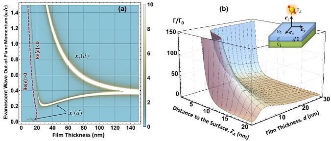
Previously, we have implemented the confinement-induced nonlocal Drude response model based on the Keldysh-Rytova (KR) pairwise electron interaction potential 2 to study theoretically the electronic properties of ultrathin TD plasmonic films 13, 14 and demonstrate their major manifestations experimentally 11, 42. The KR interaction potential takes into account the vertical electron confinement 43, 44, which makes it much stronger than the electron-electron Coulomb potential 43, offering also the film thickness as a parameter to control the electronic properties of the TD plasmonic films. Here, we use the KR model to further explore the capabilities of the TD plasmonic films, focusing on the light-scattering properties of a quantum dipole emitter (DE) placed at a distance near the film surface; see the inset in Fig. 1 (b). The model system we study mimics a quasi-2D solid-state single-photon source device, 45 for which our goal is to show the advantages of using the ultrathin TD plasmonic films. So far room-temperature solid-state quantum emitters have been observed in wide-bandgap semiconductors such as diamond 46 and silicon carbide 47, nanocrystalline quantum dots 48, 49, 50, and in carbon nanotubes 51. Single-photon emission from localized color-center defects in 2D materials has been reported both at cryogenic 52, 53, 54, 55 and at room temperatures 56, 57. An aspiring goal, however, is to use these materials in the quantum regime where the photon emission is of robust and controllable single-photon character, to enable applications in quantum information processing 45, 58. We show that the ultrathin TD plasmonic films have this outstanding potential due to their unique tailorability by means of their thickness adjustment.
Using the nanodiamond nitrogen-vacancy (NV) center 59, 60 near the TiN film surface as a prototype coupled ’DE-TD film’ system 14, we compute the spontaneous and stimulated emission intensity profiles as functions of the excitation frequency and film thickness, followed by the intensity correlation function analysis to explore the photon antibunching effect. We show that the film thickness can be used to tune from weak to strong the evanescent coupling of the DE to the plasma modes of the ultrathin TD films. The strong evanescent coupling hybridizes the transition energy levels of the DE whereby its stimulated emission is quenched. Increased resonance optical pumping reduces this quenching effect. The overall film thickness effect on the intensity correlation function is to increase its positive slope with thickness reduction and thus to improve the photon antibunching and related (nonclassical) sub-Poissonian photon counting statistics 61. Knowledge of these features is advantageous for solid-state single-photon source device engineering 45 and overall for the development of the new integrated quantum photonics material platform 62 based on the ultrathin TD materials for quantum information processing applications.
0.0.2 a. Spontaneous Emission Spectrum
Figure 1 (a) shows the earlier reported plasma mode distribution derived from the -evanescent wave reflection coefficient of the ultrathin TD plasmonic slab as a function of the thickness of the slab 14. The associated spontaneous emission rate (averaged over the three dipole orientations and normalized by the spontaneous emission rate in vacuum) is shown in Fig. 1 (b) as a function of and the DE position near the surface (see inset) where the evanescent contribution to the spontaneous emission is dominant. The DE transition frequency is taken to be eV consistent with what was reported recently from the density functional theory simulations for the zero-phonon line transition of the NV-center in diamond 60, with all other parameters being essentially representative of the ultrathin TiN film as reported earlier 14. Comparing the (a) and (b) panels, it can be clearly seen that the fast increase followed by the drop-off of the DE spontaneous emission rate at nm originates from the DE coupling to the split-off plasma mode of the lowest out-of-plane momentum which is present in there for nm. The presence itself of this split-off mode is a remarkable feature of the confinement-induced nonlocality captured by the KR model we use 14, 11.
To see how the DE coupling to the plasma modes in Fig. 1 (a) affects its spontaneous emission intensity profile, we use the analytical approach previously developed by one of us for an analogous problem of the DE coupled to a resonance of the local density of photonic states (LDOS) close to the nanotube surface 63. In our notations here, the spectral lineshape profile of the spontaneous emission intensity is given by
| (1) |
Here, the DE transition frequency includes the red shift due to the DE interaction with the surface 64 and is assumed to be dimensionless (divided by , the vacuum spontaneous emission rate 65), and so too are all quantities in the equation including the half-width-at-half maximum of the LDOS resonance. The thickness-dependent spontaneous emission rate is the one presented in Fig. 1 (b). The parameter is the Rabi-splitting to represent the DE transition level hybridization due to the coupling to the medium-assisted excitations of the material subsystem (plasma modes of the TD film herein). The coupling is termed weak if and strong if , in which cases Eq. (1) generates the single-peaked -centered Lorentzian profile and the double-picked profile of two symmetrically split peaks at , respectively 63.
0.0.3 b. Stimulated Emission Spectrum
In resonance-fluorescence experiments, the DE is irradiated by laser light tuned to the DE transition frequency, so that the DE can be excited into an upper quantum state. The excitation is followed by two competing processes. They are the (coherent) driving of the DE transition by the laser field, whereby stimulated (coherent) photon emission and absorption of a laser photon take turns, and spontaneous (incoherent) emission of the DE excited state. An interplay of the two, of which one is strongly -dependent in our case (Fig. 1), is expected to give rise to new quantum-statistical features of the scattered radiation.
It was first recognized by R.Feynmann et al. 66 that the resonance-fluorescence process can be described by optical Bloch equations, a generalization of the Bloch equations of the magnetic resonance 67, whereby the DE stimulated emission spectrum under resonance excitation can be shown to take the form as follows 65
| (2) |
Here, is the laser field frequency, is the spectral apparatus passband width, and
| (3) |
is the Laplace transform of the spectral distribution function under the resonance () single-photon transition ( is the photon occupation number) between the lower and upper DE states. In this equation, is the Rabi frequency to represent the DE transition dipole coupling strength to an external laser field, and are the longitudinal and transverse relaxation rates, respectively, analogous to those of the Bloch magnetic resonance theory 67. In our case here, we have since major relaxation comes due to spontaneous emission from the upper DE state 65. The prefactor
| (4) |
is the time-dependent upper-state occupation probability taken at . All quantities in Eqs. (2)–(4) are assumed to be dimensionless as per convention introduced above for Eq. (1).
Equations (2)–(4) allow for two distinct limiting cases 65. They are (1) the weak-driving-field limit, where to result in the -centered () single-peak Rayleigh scattering spectral profile, and (2) the high-driving-field limit, where and the spectrum is reconstructed due to the ”dressed” state formation to yield the Mollow triplet profile consisting of the -centered main peak and the two symmetric satellites at .
0.0.4 c. Intensity Correlation and Photon Antibunching
Having emitted a photon, the DE undergoes a quantum jump from the upper to the lower (ground) quantum state, whereby it can no longer emit a second photon. Only after performing a laser-induced transition back to the upper quantum state, the DE is ready to emit a second photon. The probability of emitting the first photon at an instant of time is proportional to the upper-state photon occupation probability , which also controls the intensity of the scattered light as per Eqs. (2)–(4), and which can be found from the optical Bloch equations to have the form as follows 65
| (5) |
Here
| (6) |
and the DE is assumed to be resonantly () excited out of its initial lower (ground) quantum state. Similarly, the probability of emitting a second photon at a later instant of time is proportional to the DE upper-state occupation probability under the condition that at time the DE is in its lower (ground) quantum state. Hence, the probability of emitting a first photon at time and a second photon at time is proportional to . Under the steady-state observation conditions, this turns into the two-photon scattered-intensity correlation function , a quantity directly related to the normalized second-order autocorrelation function
| (7) |
with , commonly used in single-photon source characterization experiments 56.
The function can be seen to have a positive initial slope, which reflects the quantum optics effect of photon antibunching. Clearly, the greater this slope is, the more pronounced quantum features of light are. In addition, it can be shown that since , the scattered fluorescence light gives rise to a (nonclassical) sub-Poissonian photocounting statistics 61. Both photon antibunching nature and the sub-Poissonian statistics of the resonance fluorescence from a two-level DE system may be regarded as proofs of the quantum nature of light which cannot be understood and explained in terms of classical optics.
0.0.5 d. Discussion of Numerical Results
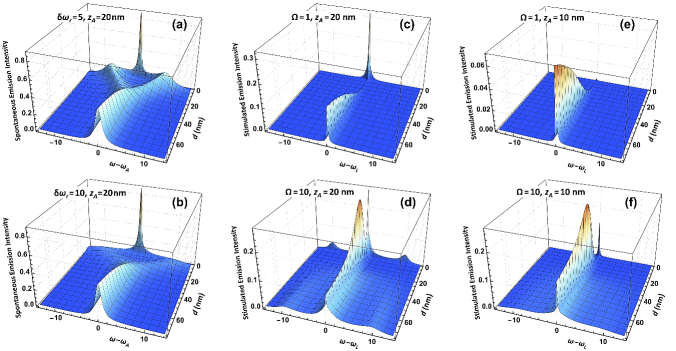
Figure 2 (a) presents the spontaneous emission spectrum calculated from Eq. (1) with (taken as a model parameter) and shown in Fig. 1 (b) for the DE positioned at nm and coupled to the TD film plasma modes shown in Fig. 1 (a). Figure 2 (b) presents the same for to compare. The most interesting feature there is that as decreases, in the domain nm, the DE-plasmon coupling strengthens to result in the fast spontaneous emission rate increase, as can be seen in Fig. 1 (b), whereby the coupled system is driven in the strong coupling regime where the new set of (hybridized) eigen levels forms 63, . This turns the single-peaked -centered Lorentzian spontaneous emission profile into the double-picked profile of the two symmetrically split resonances at . Increased does not eliminate but just smoothes out this effect. In this domain of film thicknesses, is no longer the DE eigen transition frequency, and so the intensity of the stimulated emission Rayleigh (same frequency) scattering profile drops down, as can be seen in Fig. 2 (c) for the same and , the DE radiative coupling to the external laser field. Instead, it can be shown that the plasmon enhanced Raman (shifted frequency) scattering is very efficient in this regime 68. Figure 2 (d) shows that the increased DE-laser field coupling, , can compete with the DE-plasmon coupling to restore the stimulated Rayleigh scattering intensity by driving the system in the strong radiative coupling regime with ”dressed” states formed where the representative Mollow triplet spectral profile appears. Figure 2 (e), where is decreased down to nm, demonstrates that bringing the DE closer to the film surface does drop down the intensity of the stimulated emission Rayleigh scattering profile for . The obvious reason is that the DE-plasmon coupling increases as well (not shown) so that even increased can barely restore it completely as can be seen from Fig. 2 (f). Finally, decreasing below nm restores the sharp central peaks for both spontaneous and stimulated emission profiles in Fig. 2 as only one plasma mode is found in this domain in Fig. 1 (a), which dies with decreasing to reduce as can be seen in Fig. 1 (b). This brings our system back in the weak DE-plasmon coupling regime, , followed by making it transparent in the limit.
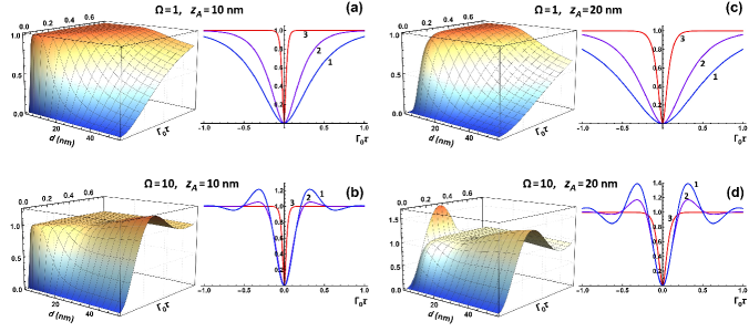
Figure 3 presents our calculations of the normalized second-order autocorrelation function of Eq. (7) for two representative and with shown in Fig. 1 (b), for the DE placed at nm and nm and coupled to the TD film plasma modes shown in Fig. 1 (a). In all four graphs, the left panels show as functions of and , while the right panels are their crosscuts by planes of constant nm (line 1), nm (line 2), and nm (line 3). There are two regimes that can be clearly seen there. They are the weak-driving-field regime and the strong-driving field regime. The former occurs for in the entire domain of presented. Here (and the two-photon scattered-intensity correlation function, accordingly) is seen to grow up monotonically from the value to approach the stationary value of , with characteristic time scale controlled by the DE spontaneous relaxation times and . The latter takes place for , where the function oscillates at Rabi frequency in the domain of moderate , with Rabi oscillations being damped due to the DE spontaneous relaxation processes. With decrease of , however, in both cases the sharp photon antibunching can be seen in the ultrathin film thickness regime. The positive initial slope of the function increases with the film thickness decrease to make the quantum single-photon features of light more pronounced for ultrathin TD films.
0.0.6 Conclusion
In this work we use the parameters of the nanodiamond NV center near the TiN film surface to compute the spontaneous and stimulated emission intensity profiles as functions of the excitation frequency and film thickness, followed by the intensity correlation function analysis to explore the photon antibunching effect for the quantum DE coupled the ultrathin TD plasmonic film. We show that the film thickness can be used to tune the evanescent coupling of the DE to the plasma modes of the film. The strong evanescent coupling hybridizes the transition energy levels of the DE, whereby its stimulated emission Rayleigh scattering profile is quenched. Increased resonance optical pumping drives the system in the strong radiative coupling regime, which competes with the DE-plasmon coupling, to restore the stimulated Rayleigh scattering intensity. The overall film thickness effect on the second-order photon autocorrelation function is to increase its positive slope with thickness reduction and thus to improve the photon antibunching properties and related (nonclassical) sub-Poissonian photon counting statistics. Knowledge of these features is advantageous for solid-state single-photon source device engineering and overall for the development of the new integrated quantum photonics material platform based on the ultrathin TD materials for quantum information processing applications.
This research is supported by the U.S. National Science Foundation under Condensed Matter Theory Program Award No. DMR-1830874 (I.V.B.). I.V.B. acknowledges hospitality of the Kavli Institute for Theoretical Physics (KITP), UC Santa Barbara, where this work was completed during his invited visit as a KITP Fellow 2022–23 (the research program supported by the U.S. National Science Foundation under Grant No. PHY-1748958).
References
- 1 N.Rivera, I.Kaminer, B.Zhen, J.D.Joannopoulos, and M.Soljaić, Shrinking light to allow forbidden transitions on the atomic scale, Science 353, 263 (2016).
- 2 I.V.Bondarev and V.M.Shalaev, Universal features of the optical properties of ultrathin plasmonic films, Optical Mater. Express 7, 3731 (2017).
- 3 A.Boltasseva and V.M.Shalaev, Transdimensional photonics, ACS Photon. 6, 1 (2019).
- 4 A.Kossoy, V.Merk, D.Simakov, K.Leosson, S.Kéna-Cohen, and S.A.Maier, Optical and structural properties of ultra-thin gold films, Adv. Opt. Mater. 3, 71 (2015).
- 5 J.Halim, S.Kota, M.R.Lukatskaya, M.Naguib, M.-Q.Zhao, E.J.Moon, J.Pitock, J.Nanda, S.J.May, Y.Gogotsi, M.W.Barsoum, Synthesis and characterization of 2D molybdenum carbide (MXene), Adv. Funct. Mater. 26, 3118 (2016).
- 6 D.Shah, H.Reddy, N.Kinsey, V.M.Shalaev, and A.Boltasseva, Optical properties of plasmonic ultrathin TiN films, Adv. Optical Mater. 5, 1700065 (2017).
- 7 D.Shah, A.Catellani, H.Reddy, N.Kinsey, V.M.Shalaev, A. Boltasseva, and A. Calzolari, Controlling the plasmonic properties of ultrathin tin films at the atomic level, ACS Photon. 5, 2816 (2018).
- 8 A.Rodríguez Echarri, J.D.Cox, and F.J.García de Abajo, Quantum effects in the acoustic plasmons of atomically thin heterostructures, Optica 6, 630 (2019).
- 9 Z.M.Abd El-Fattah, V.Mkhitaryan, J.Brede, L.Fern?ndez, C.Li, Q.Guo, A.Ghosh, A.Rodríguez Echarri, D.Naveh, F.Xia, J.Enrique Ortega, and F.J.García de Abajo, Plasmonics in atomically thin crystalline silver films, ACS Nano 13, 7771 (2019).
- 10 R.A.Maniyara, D.Rodrigo, R.Yu, J.Canet-Ferrer, D.S.Ghosh, R.Yongsunthon, D.E.Baker, A.Rezikyan, F.J.García de Abajo, and V.Pruneri, Tunable plasmons in ultrathin metal films, Nature Photonics 13, 328 (2019).
- 11 D.Shah, M.Yang, Z.Kudyshev, X.Xu, V.M.Shalaev, I.V.Bondarev, and A.Boltasseva, Thickness-dependent Drude plasma frequency in transdimensional plasmonic TiN, Nano Lett. 22, 4622 (2022).
- 12 X.Liu, J.-H.Kang, H.Yuan, J.Park, S.J.Kim, Y.Cui, H.Y.Hwang, and M.L.Brongersma, Electrical tuning of a quantum plasmonic resonance, Nature Nanotechnology 12, 866 (2017).
- 13 I.V.Bondarev, H.Mousavi, and V.M.Shalaev, Optical response of finite-thickness ultrathin plasmonic films, MRS Commun. 8, 1092 (2018).
- 14 I.V.Bondarev, H.Mousavi, and V.M.Shalaev, Transdimensional epsilon-near-zero modes in planar plasmonic nanostructures, Phys. Rev. Research 2, 013070 (2020).
- 15 L.Zundel, P.Gieri, S.Sanders, and A.Manjavacas, Comparative analysis of the near- and far-field optical response of thin plasmonic nanostructures, Adv. Optical Mater. 10, 2102550 (2022).
- 16 A.Manjavacas and F.J.Garcia de Abajo, Tunable plasmons in atomically thin gold nanodisks, Nature Commun. 5, 3548 (2014).
- 17 F.J.Garcia de Abajo and A.Manjavacas, Plasmonics in atomically thin materials, Faraday Discuss. 178, 87 (2015).
- 18 S.Campione, I.Brener, and F.Marquier, Theory of epsilon-near-zero modes in ultrathin films, Phys. Rev. B 91, 121408(R) (2015).
- 19 I.V.Bondarev, Finite-thickness effects in plasmonic films with periodic cylindrical anisotropy [Invited], Optical Mater. Express 9, 285 (2019).
- 20 I.V.Bondarev and C.M.Adhikari, Collective excitations and optical response of ultrathin carbon-nanotube films, Phys. Rev. Applied 15, 034001 (2021).
- 21 C.M.Adhikari and I.V.Bondarev, Controlled exciton-plasmon coupling in a mixture of ultrathin periodically aligned single-wall carbon nanotube arrays, J. Appl. Phys. 129, 015301 (2021).
- 22 B.Miller, A.Steinhoff, B.Pano, J.Klein, F.Jahnke, A.Holleitner, and U.Wurstbauer, Long-lived direct and indirect interlayer excitons in van der Waals heterostructures, Nano Lett. 17, 5229 (2017).
- 23 I.V.Bondarev and M.R.Vladimirova, Complexes of dipolar excitons in layered quasi-two-dimensional nanostructures, Phys. Rev. B 97, 165419 (2018).
- 24 T.Deilmann and K.S.Thygesen, Interlayer trions in the MoS2/WS2 van der Waals heterostructure, Nano Lett. 18, 1460 (2018).
- 25 L.A.Jauregui, A.Y.Joe, K.Pistunova, D.S.Wild, A.A. High, Y.Zhou, G.Scuri, K.De Greve, A.Sushko, C.-H.Yu, T.Taniguchi, K.Watanabe, D.J.Needleman, M.D.Lukin, H.Park, and P.Kim, Electrical control of interlayer exciton dynamics in atomically thin heterostructures, Science 366, 870 (2019).
- 26 E.V.Calman, L.H.Fowler-Gerace, D.J.Choksy, L.V.Butov, D.E.Nikonov, I.A.Young, S.Hu, A.Mishchenko, and A.K.Geim, Indirect excitons and trions in MoSe2/WSe2 van der Waals heterostructures, Nano Lett. 20, 1869 (2020).
- 27 I.V.Bondarev, O.L.Berman, R.Ya.Kezerashvili, and Y.E.Lozovik, Crystal phases of charged interlayer excitons in van der Waals heterostructures, Communications Physics 4, 134 (2021).
- 28 X.Wang, J.Zhu, K.L.Seyler, P.Rivera, H.Zheng, Y.Wang, M.He, T.Taniguchi, K.Watanabe, J.Yan, D.G.Mandrus, D.R.Gamelin, W.Yao, and X.Xu, Moiré trions in MoSe2/WSe2 heterobilayers, Nature Nanotechn. 16, 1208 (2021).
- 29 Z.Sun, J.Beaumariage, Q.Wan, H.Alnatah, N.Hougland, J.Chisholm, Q.Cao, K.Watanabe, T.Taniguchi, B.M.Hunt, I.V.Bondarev, and D.Snoke, Charged bosons made of fermions in bilayer structures with strong metallic screening, Nano Lett. 21, 7669 (2021).
- 30 J.Pelliciari, S.Lee, K.Gilmore, J.Li, Y.Gu, A.Barbour, I.Jarrige, C.H.Ahn, F.J.Walker, and V.Bisogni, Tuning spin excitations in magnetic films by confinement, Nature Materials 20, 188 (2021).
- 31 A.M.Dubrovkin, B.Qiang, H.N.S.Krishnamoorthy, N.I.Zheludev, and Q.J.Wang, Ultra-confined surface phonon polaritons in molecular layers of van der Waals dielectrics, Nature Commun. 9, 1762 (2018).
- 32 K.P.Kelley, T.G.Folland, J.Ryan Nolen, N.Engheta, J.D.Caldwell, and J.-P.Maria, Polaritonic hybrid-epsilon-near-zero modes: Beating the plasmonic confinement vs propagation-length trade-off with doped cadmium oxide bilayers, Nano Lett. 19, 948 (2019).
- 33 R.H.Ritchie, Plasma losses by fast electrons in thin films, Phys. Rev. 106, 874 (1957).
- 34 E.N.Economou, Surface plasmons in thin films, Phys. Rev. 182, 539 (1969).
- 35 D.A.Dahl and L.J.Sham, Electrodynamics of quasi-two-dimensional electrons, Phys. Rev. B 16, 651 (1977).
- 36 T.N.Theis, Plasmons in inversion layers, Surf. Sci. 98, 515 (1980).
- 37 T.Ando, A.B.Fowler, and F.Stern, Electronic properties of two-dimensional systems, Rev. Mod. Phys. 54, 437 (1982).
- 38 A.V.Chaplik, Absorption and emission of electromagnetic waves by two-dimensional plasmons, Surf. Sci. Rep. 5, 289 (1985).
- 39 Z.L.Wang, Valence electron excitations and plasmon oscillations in thin films, surfaces, interfaces and small particles, Micron 27, 265 (1996).
- 40 J.M.Pitarke, V.M.Silkin, E.V.Chulkov, and P.M.Echenique, Theory of surface plasmons and surface-plasmon polaritons, Rep. Prog. Phys. 70, 1 (2007).
- 41 A.Politano and G.Chiarello, Plasmonic modes in thin films: quo vadis?, Front. Mater. 1, 9 (2014).
- 42 L.Vertchenko, L.Leandro, E.Shkondin, O.Takayama, I.V.Bondarev, N.Akopian, and A.V.Lavrinenko, Cryogenic characterization of titanium nitride thin films, Optical Mater. Express 9, 2117 (2019).
- 43 L.V.Keldysh, Coulomb interaction in thin semiconductor and semimetal films, Pis’ma Zh. Eksp. Teor. Fiz. 29, 716 (1979) [Engl. translation: JETP Lett. 29, 658 (1980)].
- 44 N.S.Rytova, Screened potential of a point charge in a thin film, Moscow University Physics Bulletin 3, 30 (1967).
- 45 M.Kianinia, Z.-Q.Xu, Milos Toth, and I.Aharonovich, Quantum emitters in 2D materials: Emitter engineering, photophysics, and integration in photonic nanostructures, Appl. Phys. Rev. 9, 011306 (2022).
- 46 I.Aharonovich and E.Neu, Diamond nanophotonics, Adv. Opt. Mater. 2, 911 (2014).
- 47 S.Castelletto, B.C.Johnson, V.Ivády, N.Stavrias, T.Umeda, A.Gali, and T.Ohshima, A silicon carbide room-temperature single-photon source, Nature Mater. 13, 151 (2014).
- 48 B.D.Mangum, F.Wang, A.M.Dennis, Y.Gao, X.Ma, J.A.Hollingsworth, and H.Htoon, Competition between Auger recombination and hot-carrier trapping in PL intensity fluctuations of type II nanocrystals, Small 10, 2892 (2014).
- 49 F.Pisanello, G.Leménager, L.Martiradonna, L.Carbone, S.Vezzoli, P.Desfonds, P.D.Cozzoli, J.-P.Hermier, E.Giacobino, R.Cingolani, M.De Vittorio, and A.Bramati, Non-blinking single-photon generation with anisotropic colloidal nanocrystals: Towards room-temperature, efficient, colloidal quantum sources. Adv. Mater. 25, 1974 (2013).
- 50 P.Michler, A.Imamolu, M.D.Mason, P.J.Carson, G.F.Strouse, and S.K.Buratto, Quantum correlation among photons from a single quantum dot at room temperature, Nature 406, 968 (2000).
- 51 X.Ma, N.F.Hartmann, J.K.Baldwin, S.K.Doorn, and H.Htoon, Room-temperature single-photon generation from solitary dopants of carbon nanotubes. Nature Nanotech. 10, 671 (2015).
- 52 C.Chakraborty, L.Kinnischtzke, K.M.Goodfellow, R.Beams, and A.N.Vamivakas, Voltage-controlled quantum light from an atomically thin semiconductor. Nature Nanotechnology 10, 507 (2015).
- 53 Y.-M.He, G.Clark, J.R.Schaibley, Y.He, M.-C.Chen, Y.-J.Wei, X.Ding, Q.Zhang, W.Yao, X.Xu, C.-Y.Lu, and J.-W.Pan, Single quantum emitters in monolayer semiconductors, Nature Nanotechnology 10, 497 (2015).
- 54 M.Koperski, K.Nogajewski, A.Arora, V.Cherkez, P.Mallet, J.-Y.Veuillen, J.Marcus, P.Kossacki, and M.Potemski, Single photon emitters in exfoliated WSe2 structures, Nature Nanotechnology 10, 503 (2015).
- 55 A.Srivastava, M.Sidler, A.V.Allain, D.S.Lembke, A.Kis, and A.Imamolu, Optically active quantum dots in monolayer WSe2, Nature Nanotechnology 10, 491 (2015).
- 56 T.T.Tran, K.Bray, M.J.Ford, M.Toth, and I.Aharonovich, Quantum emission from hexagonal boron nitride monolayers, Nature Nanotechnology 11, 37 (2016).
- 57 A.Dietrich, M.W.Doherty, I.Aharonovich, and A.Kubanek, Solid-state single photon source with Fourier transform limited lines at room temperature, Phys. Rev. B 101, 081401(R) (2020).
- 58 J.L.OBrien, A.Furusawa, and J.Vuković, Photonic quantum technologies. Nature Photon. 3, 687 (2009).
- 59 S.I.Bogdanov, M.Y.Shalaginov, A.S.Lagutchev, C.-C Chiang, D.Shah, A.S.Baburin, I.A.Ryzhikov, I.A.Rodionov, A.V.Kildishev, A.Boltasseva, and V.M.Shalaev, Ultrabright room-temperature sub-nanosecond emission from single NV-centers coupled to nanopatch antennas, Nano Lett. 18, 4837 (2018).
- 60 R.Löfgren, S.Öberg, and J.A.Larsson, The diamond NV-center transition energies in the vicinity of an intrinsic stacking fault, AIP Advances 12, 035009 (2022).
- 61 R.J.Cook, Photon number statistics in resonance fluorescence, Phys. Rev. A 23, 1243 (1981).
- 62 S.Bogdanov, M.Y.Shalaginov, A.Boltasseva, and V.M.Shalaev, Material platforms for integrated quantum photonics, Optical Mater. Express 7, 111 (2017).
- 63 I.V.Bondarev and B.Vlahovich, Optical absorption by atomically doped carbon nanotubes, Phys. Rev. B 74, 073401 (2006).
- 64 I.V.Bondarev and Ph.Lambin, van der Waals coupling in atomically doped carbon nanotubes, Phys. Rev. B 72, 035451 (2005).
- 65 W.Vogel and D.-G.Welsch, Quantum Optics (Wiley-VCH, New York, 2006).
- 66 R.P.Feynman, F.L.Vernon, and R.W.Hellwarth, Geometrical representation of the Schrödinger equation for solving maser problems, J. Appl. Phys. 28, 49 (1957).
- 67 K.Bloom, Density Matrix Theory and Applications (Springer-Verlag, Berlin, 2012).
- 68 I.V.Bondarev, Plasmon enhanced Raman scattering effect for an atom near a carbon nanotube, Optics Express 23, 3971 (2015).