Frequency-Encoded Deep Learning
with Speed-of-Light Dominated Latency
Abstract
The ability of deep neural networks to perform complex tasks more accurately than manually-crafted solutions has created a substantial demand for more complex models processing larger amounts of data. However, the traditional computing architecture has reached a bottleneck in processing performance due to data movement from memory to computing. Considerable efforts have been made towards custom hardware acceleration, among which are optical neural networks (ONNs). These excel at energy efficient linear operations but struggle with scalability and the integration of linear and nonlinear functions. Here, we introduce our multiplicative analog frequency transform optical neural network (MAFT-ONN) that encodes the data in the frequency domain to compute matrix-vector products in a single-shot using a single photoelectric multiplication, and then implements the nonlinear activation for all neurons using a single electro-optic modulator. We experimentally demonstrate a 3-layer DNN with our architecture using a simple hardware setup assembled with commercial components. Additionally, this is the first DNN hardware accelerator suitable for analog inference of temporal waveforms like voice or radio signals, achieving bandwidth-limited throughput and speed-of-light limited latency. Our results demonstrate a highly scalable ONN with a straightforward path to surpassing the current computing bottleneck, in addition to enabling new possibilities for high-performance analog deep learning of temporal waveforms.
Introduction
DNNs are revolutionizing computing and signal processing in applications ranging from image classification and autonomous robotics to life science [1, 2, 3, 4]. However, exponentially increasing DNN parameters over the last 20 years [5] and the large quantities of data are stretching the limits of present-day conventional computing architectures, primarily due to the “von Neumann” bottleneck in data movement from memory to processing [6]. Numerous approaches are looking to address this bottleneck by different computing paradigms like the Google Tensor Processing Unit (TPU), SRAM, DRAM, and memristor architectures that increase throughput by merging together the memory operations and matrix computations into single hardware elements [6].
Optical systems promise DNN acceleration by encoding, routing, and processing analog signals in optical fields, allowing for operation at the quantum-noise-limit with high bandwidth and low energy consumption. Optical neural network (ONN) schemes rely on (i) performing linear algebra intrinsically in the physics of optical components and/or (ii) in-line nonlinear transformations . For (i), past approaches include Mach-Zehnder interferometer (MZI) meshes [7, 8, 9, 10], on-chip micro-ring resonators (MRRs) [11, 12, 13, 14], wavelength-division multiplexing (WDM) [15, 16, 17], photoelectric multiplication [18], spatial light modulation [19, 20, 21, 22, 23, 24], optical scattering [25], and optical attenuation [26]. For (ii), past approaches include optical-electrical-optical (OEO) elements [27, 28, 29, 26] and all-optical [23, 30, 31, 32, 13, 33] approaches. However, to fully take advantage of the potential ultra-low latency and energy consumption available in photonics, it is necessary to implement linear and nonlinear operations together with minimal overhead. Simultaneously achieving (i) and (ii) in a way that preserves high hardware scalability and performance has been an open challenge.
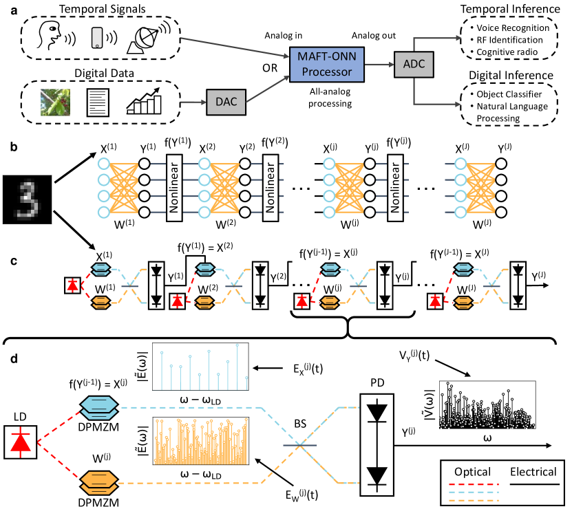
Our multiplicative analog frequency transform optical neural network (MAFT-ONN) architecture simultaneously achieves (i) and (ii) for DNN inference with arbitrary scalability in DNN size and layer depth. We experimentally demonstrate the MAFT-ONN in a 3-layer DNN for inference of MNIST images. In this architecture, we encode neuron values in the amplitude and phase of frequency modes, and ‘photoelectric multiplication’ [18] performs matrix-vector products in a single shot. In a proof-of-concept experiment with commercial components, we realize the MAFT-ONN scheme that combines efficient optical matrix operations with in-line nonlinear transformations by electro-optic nonlinearities, enabling a scalable front-to-back photonic hardware accelerator for DNNs. This architecture enables DNN inference for an arbitrary number of layers using a simple hardware setup that maintains high throughput and ultra-low latency, which are important performance metrics for applications like voice recognition, spectral channel monitoring, distributed sensing, and cognitive radio. Figure 1(a) contextualizes use-cases for the MAFT-ONN processor.
MAFT-ONN Architecture
As illustrated in Figure 1(b), a generic DNN consists of an input layer, at least one hidden layer, and an output layer that yields the processed data. As seen in Figure 1(c), these DNN layers map to a series of photonic hardware layers, indexed here from . Figure 1(d) details an arbitrary layer with input and output neurons. Thus, the input vector has size , the weight matrix has size , and the output vector has size .
Matrix algebra: The values of , , and are all contained in frequency-encoded signals. The input vector to layer , , begins as an optical field , which is the result of modulating a laser diode (labeled LD) via a dual-parallel Mach-Zehnder modulator (DPMZM) that is driven by the photovoltage output of the previous layer . Let the neuron values of have a frequency spacing and offset . Then the frequency encoded signal for is:
where is the laser frequency.
The weight matrix also begins as an electrical signal, . We choose to encode so that the output vector has frequency spacing and offset . After modulating on a DPMZM, the weight matrix optical field is:
Figure 1(d) plots the frequency content of the optical input and weights , where the tilde over a variable indicates its Fourier Transform. Note that both of these signals are single-sideband with respect to the laser carrier.
Sending and through a 50:50 beamsplitter (labeled BS) onto a balanced photodetection apparatus (labeled PD) produces a photovoltage
| (1) | ||||
| (2) |
where we ignore linear scaling factors here (see the Discussion section for the link gain analysis). Here, the partial sums of coherently summed in the frequency domain to yield the desired matrix product in a single shot:
| (3) |
Thus, this MAFT scheme transforms an input signal with frequency spacing into an output signal with spacing while simultaneously computing a matrix-vector product. The signal contains ‘spurious frequencies’ that do not contribute to the matrix-vector product. In practice, we eliminate using passive RF bandpass filters or RF cavities/optical ring resonators with a free-spectral range equal to . However, in DNN training, we found a benefit to retaining , as discussed later. For a more detailed and generalized derivation of the MAFT scheme, see Supplementary Section E.
Nonlinear activation: We achieve the nonlinear activation by applying to the nonlinear regime of an MZM, yielding the optical input to the next layer :
| (4) |
Here, contributes to the DC offset; depends on the laser power, insertion loss, and propagation loss; depends on the and efficiency of the MZM; and depends on the bias conditions and inherent bias point of the MZM. Using these four parameters, we can program the strength of the nonlinearity. The function is the analytic Hilbert transform, which removes the negative frequency components from the sinusoids (making them complex-valued) to ensure that is single-sideband with respect to the laser carrier, as and are. Therefore, the MZM simultaneously encodes the next layer’s input vector while also implementing the nonlinear transformation on .
The Fourier transform of (written in the time domain in Equation 4) reveals an unusual property of : the nonlinearity applied to one neuron depends on all neurons via an expression of the form . Whereas for a conventional DNN, acts element-wise on each vector component. We incorporated this ‘all-to-all’ nonlinearity into our training procedure (see below) for the conventional DNN tasks considered in this work, but note that other works call for such data-dependent nonlinear activations for applications like adversarial DNNs [34].
Remarks: (i) The MAFT scheme presented here readily extends to matrix-matrix multiplication via time or frequency-multiplexing of the input vector . For time-multiplexing, we append input vectors in the time domain, which corresponds to batching several inputs to be inferred by the same weight matrix. See Supplementary Section J for more details. For frequency-multiplexing, see Figure 4(a). (ii) Note that in this analysis, all frequencies are equally spaced to maximize the throughput of the matrix-vector computations.
Matrix Experimental Demonstration
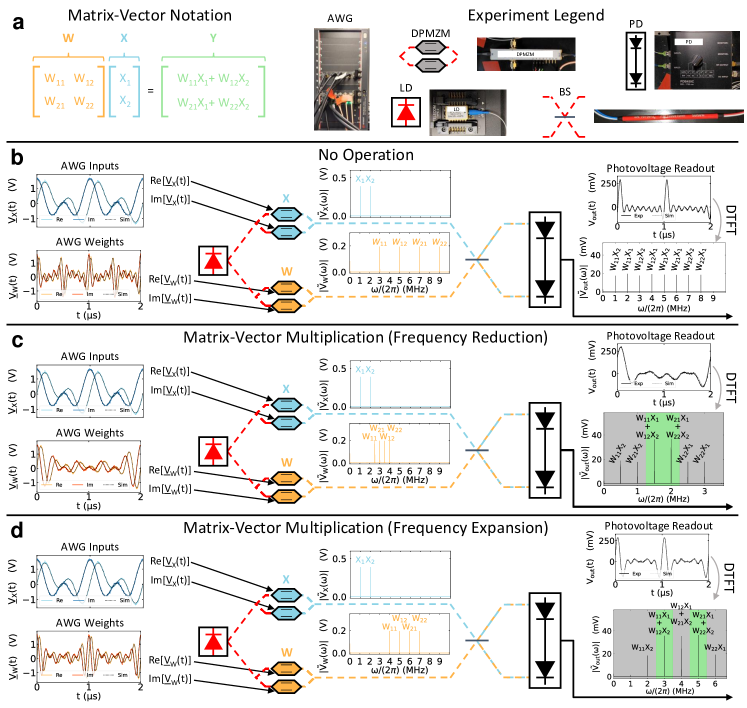
Figure 2 walks though an experimental example of a matrix-vector multiplication using the MAFT scheme. Figure 2(a) keeps track of all the matrix and partial sum elements. The input and weight electrical voltage signals and , respectively, were generated by an arbitrary waveform generator (AWG) and then sent to DPMZMs. These DPMZMs perform single-sideband suppressed carrier (SSB-SC) modulation of the signals, without which the modulated signals would be dual-sideband and completely cancel each other out after the photoelectric multiplication. To SSB-SC modulate an arbitrary signal, one copy of the signal is sent to one of the sub-MZMs of the DPMZM, and another phase-shifted copy is sent to the other sub-MZM. Thus, let an underbar indicate an analytical Hilbert transform, yielding . Then is the original signal, and is the phase-shifted copy. Figure 2 illustrates both signals in the time domain since they have the same magnitude in the frequency domain. (Although the phase-shifted was generated using an AWG in this experiment, in deep neural nets this phase shift can be achieved using commercial wide-band passive RF phase shifters.)
In this example, contains two frequencies, contains four frequencies, and the output electrical voltage signal contains a variable number of frequencies. We keep the same while altering to demonstrate various effects. In Figure 2(b), is programmed so that each partial sum in maps to a unique frequency, thus performing no summation in the frequency domain. In Figure 2(c), is programmed so that the frequency domain of yields a matrix-vector product where the frequencies corresponding to the elements of are adjacently spaced in the middle of the spurious frequencies. We refer to this method of programming as our frequency reduction scheme because . Figure 2(d) demonstrates an alternative method of programming , which intersperses the elements of with the spurious frequency components. We term this the frequency expansion scheme, as . The frequency reduction and expansion schemes can be used alternatively for consecutive layers of a DNN to avoid running out of bandwidth. Alternatively, as demonstrated by the experiment in the next section, we can keep the spurious frequency components for training the DNN, which avoids the requirement for filters that precisely match the neuron frequencies.
Experiment
Experimental Apparatus
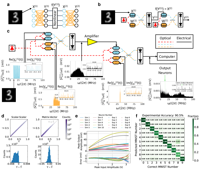
We experimentally demonstrated the MAFT-ONN scheme using the apparatus shown in Figure 3(c). An AWG generates , , and , all of which are modulated into the optical domain using DPMZMs. The frequency reduction scheme from Figure 2(c) was used to program , yielding after the first layer. We decided to keep the spurious frequencies for DNN training, so . We then amplify to reach the nonlinear regime of the DPMZM in the second layer, after which it became the optical input signal to the second layer. For convenience, we only used one sub-modulator of the DPMZM for this signal, thus modulating in the dual-sideband suppressed carrier (DSB-SC) mode. For the second layer, we programmed using the frequency expansion scheme from Figure 2(d). The multiplication of the DSB-SC modulated and the SSB-SC modulated results in a copy of appearing further up in the spectrum, as can be seen in the plot of in Figure 3(c). Finally, the analog output of the second layer was sampled digitally and Fourier transformed. See Supplementary Section A for more details on the 3-layer DNN experimental setup.
Linear Characterization
To test linear matrix-vector multiplication, we measure the photovoltage response using a spectrum analyzer that scans the relevant part of the bandwidth to extract . Here, the input laser is modulated by and via DPMZMs in the linear regime. We repeat this multiplication over randomized values of and to obtain the full set of characterization data.
To measure the accuracy of the matrix products, we use a theoretical model to compare with the experiment. From Equation 4, the result of linearly modulating the input vector is:
where we assume that in the linear regime. Similarly, the linear modulation of the weight matrix yields . Therefore from Equation 1, the resulting photoelectric multiplication is:
where is determined by the responsivity of the photodetector and the termination resistance.
Hence for the linear characterization, we use a 1-parameter curve fit where the parameter estimates the value of . To attain the curve fit parameter, we used a single randomized matrix-vector product and gradually increased the amplitude to create a curve, where the slope of the curve is determined by . We re-calibrated the curve fit whenever we changed the size of the matrix-vector product being experimentally computed. See Supplementary Section B for more details on the statistical linear curve fitting methods.
Figure 3(d) shows the experimental matrix-vector multiplication performance of our architecture, where is the expected curved-fitted value of the output vector, and is the experimental output vector. Both and are normalized to the largest value among all the products. First, we characterized scalar-scalar products by computing 10,000 randomized scalar-scalar multiplications and comparing them to the curve fitted analytical product, yielding 9-bit precision. Next, we computed 10,000 randomized matrix-vector products to yield 8-bit precision. Thus, we achieved accurate experimental linear matrix-vector products using this architecture.
Nonlinear Characterization
Figure 3(e) illustrates a nonlinear curve fit for a simple intensity-modulated direct detection (IMDD) link, which consists of an electrical input signal being modulated by an MZM and then immediately detected with a photodetector. Our equation that models the output of the IMDD link is:
| (5) |
Thus, we use a 4-parameter curve fit for the nonlinear characterization (counting as a single parameter). Figure 3(e) shows an example of curve fitting the analytical model to an experimental characterization of an MZM, where is a input vector. For more details and other nonlinear curve fit characterizations, see Supplementary Section C.
3-Layer DNN Inference
We experimentally demonstrated a proof-of-concept of the MAFT-ONN architecture for a 3-layer DNN trained to classify MNIST digits, as shown in Figure 3(a). The outline of the setup is referenced in Figure 3(b), where each photoelectric multiplication implements a fully connected layer, and the modulator of the second layer implements the nonlinear activation. The first layer uses downsampled MNIST images as the input activations, represented by a frequency-encoded signal containing 196 frequencies spaced at 100 kHz. The input activation is followed by a hidden layer of 100 neurons represented by a weight signal containing 19,600 frequencies spaced at 1 kHz. The final layer has 10 neurons, one for each of the MNIST digits, and thus the second layer weight signal contains 1,000 frequencies spaced at 1 kHz. As previously mentioned, we did not filter out the spurious frequencies, and thus trained our DNN on nearly 2 million partial sums.
We implemented the one-hot vector that represents the output MNIST values by randomly selecting a set of 10 adjacent frequencies among the spurious frequencies of , to demonstrate the flexibility of our scheme. (See Supplementary Section I for an analysis of choosing random parts of the spectrum for DNN training.) The 10 output neuron frequencies were randomly chosen to be 14.03 MHz to 14.039 MHz, with 1 kHz spacing. The zoom of the plot of in Figure 3(c) shows the mapping of the neuron frequencies to the MNIST digits, where the digit is classified by the frequency mode with that largest magnitude.
Since this scheme performs coherent interferometry, we programmed positive and negative neuron values into both the input vectors and weight matrices. Negative neuron values are physically represented by a phase shift in that particular frequency mode, allowing for analog matrix algebra with negative numbers.
An analytic model of the hardware was used to train the DNN offline, similar to the nonlinear characterization in the previous section. The offline training produced a set of weight matrices that were then encoded into the RF signals used for the experimental inferences. See Supplementary Sections C and D for details on the offline DNN characterization and training.
The 3-layer experimental DNN inferred 200 MNIST images, where the digital DNN has an accuracy of 95.5% and the experimental DNN has an accuracy of 90.5%. One contribution to the experimental inaccuracy is the uneven frequency responses of the DPMZMs across the broad bandwidth (see Supplementary Section B), which can be deterministically characterized, improving the accuracy. A higher power low-noise amplified balanced photodetector would also increase the SNR of the signal going into the second layer. Additionally, performing the DNN training in-situ on the hardware itself [35] could help better characterize it and increase the accuracy. The confusion matrix of the experimental DNN is shown in Figure 3(f).
Thus, we have demonstrated for the first time a scalable ONN that implements both the linear and nonlinear operations in-line, where one interferometer implements the single-shot matrix-vector product and one modulator implements the nonlinear activation for an entire layer, enabling scalability in DNN width. In addition, the MAFT-ONN is also scalable in DNN depth due to the ability to directly send the analog output of one layer as the input to the next layer for an arbitrary number of layers, all without digital processing.
Discussion
Time-based Signal Processing
To our knowledge, this MAFT scheme is the first DNN hardware accelerator that is suitable for the direct inference of time-based signals like radio, voice recognition, and biological waveforms, as they are already frequency-encoded when considering their Fourier transform. In current DNN and ONN architectures, running inference for time-based signals requires the signal to be digitized and pre-processed to be compatible with the hardware, and one must choose how to handle complex-valued data. For example, for RF signal processing, some works process the raw digital IQ data [36], some hand-pick features [37], and some convert the time-based signal into an image using a spectrogram [38]. All of these approaches require digital processing before inference, which is problematic for real-time applications like cognitive radio, voice recognition, and self-driving cars, where ultra-low latency and high-bandwidth throughput are essential.
Computational Throughput
The throughput measures the number of multiply-and-accumulates (MACs) computed within a given time. The number of MACs performed in a fully connected layer with input neurons and output neurons is . The time it takes to read out the output vector is the latency, which is , where is the smallest frequency spacing of the output signal and is the lowest neuron frequency of the output signal. (Note that , where is the angular frequency from the previous sections.) This is also the same as the period of the input, weight, and output signals, and thus the minimum time it takes to create the frequency-encoded signals. Therefore, the throughput is:
Let be the bandwidth available to modulate the input and weight signals. We calculate the throughput in terms of by plugging in the values of and based on how the inputs and weight frequencies are programmed. The specific method of programming the inputs and weights is determined by the anti-aliasing conditions that preserve the integrity of the matrix product after the photoelectric multiplication. See Supplementary Section F for the derivation of the anti-aliasing conditions. This analysis yields the throughputs of the frequency reduction and expansion schemes, respectively:
| (6) | ||||
| (7) |
The approximations for Equations 6 and 7 are valid for and , respectively. Therefore, the maximum throughput of this architecture is ultimately limited by the available bandwidth, independent of DNN size. This is because for a given bandwidth limitation , as the number of neurons increase, the frequency spacing must correspondingly decrease to keep all of the frequencies within the bandwidth. This trade-off yields very similar throughput regardless of the number of neurons or frequency spacing.
In our experiment, we did not filter the signal after layer 1, meaning that we used all the spurious frequencies for DNN training. Note that each spurious frequency contains unique partial sums that are not present in the original matrix-vector product, which is additional information content. Thus, if the throughput calculation were to include these spurious frequencies, then it would be:
This spurious throughput is unbounded in , because in this case, the trade-off from decreasing the frequency spacing to allow for more neurons always results in higher throughput. (Note that the spurious throughput only yields a logarithmic advtange in when comparing to an operation like the convolution, which uses DTFTs for efficient computation.) Here, the limiting factor is the linewidth of each frequency mode that would prevent adjacent frequencies from being resolved. See Supplementary Section G for the full throughput derivation.
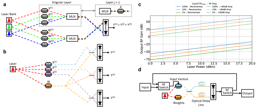
The bandwidth limiting the throughput is not the RF bandwidth of the electrical components, but the available optical bandwidth. The maximum throughput of this architecture can be realized by: (i) optical wavelength-division multiplexing (WDM) the frequency-encoded signals, or (ii) replacing the frequency-encoded signals with optical frequency combs. For (i), Figure 4(a) illustrates a variant of this architecture that uses optical WDM to simultaneously perform multiple matrix-vector products on each laser on the same photodetector. The incoherence between the lasers allows for each matrix-vector product to independently sum at the photovoltage output. As long as the gap between each laser wavelength is greater than the bandwidth of the photodetector, there will be no cross coupling terms between the matrix-vector products performed on each laser carrier. With the WDM version of the architecture, large matrix products can be tiled in the frequency domain, or matrix-matrix products can be frequency-multiplexed while still computing everything in a single shot. The optical bandwidth can also be used in the case of an arbitrarily deep neural network (the box labeled “Layer ” in Figure 4(a)), where the same input vector can be independently multiplied by different weight signals for applications like convolution. There is more than 20 THz of available bandwidth among the S, C, and L telecommunication bands (1460nm-1625nm) that can be used here for optical WDM. For (ii), optical frequency combs can replace the WDM modules in Figure 4(a) for even larger throughput. Other works have experimentally demonstrated optical frequency combs with almost 1,000 THz bandwidth [39, 40]. An optical AWG or waveshaper would be required to program the frequency combs.
The thoughput can be further increased through spatial multiplexing with copies of the setup running in parallel, shown in Figure 4(b). Other works have demonstrated the viability of densely-packed MZMs, such as a photonic integrated circuit with 48 on-chip MZMs [41]. Therefore, the combination of using the full optical bandwidth (on the order of terahertz) and spatial multiplexing (on the order of a hundred) immediately yields a straightforward path to reaching peta-operation per second scale throughputs with current technology. Thus, the MAFT-ONN is competitive with electronic counterparts like the Google TPUv3 that has a throughput greater than 400 tera-operations per second [42].
Note that this throughput analysis assumes that the optical bandwidth is the limiting factor in throughput. See Supplementary Section H for a throughput derivation that is limited to only the electronics without using optical WDM.
Physical Latency
The physical latency of this architecture is the time it takes for a signal that is already frequency-encoded to enter the system, go through the optical processing, and then physically leave the system as an electrical output vector signal. (Thus, the time it takes for the signal to travel from the “Analog in” to “Analog out” in Figure 1(a).) This is different from the readout latency described earlier, which is the time it takes to distinguish the frequency modes of the output vector signal. The physical latency of the system in Figure 1(c) with DNN layers is: , where is the reciprocal of the bandwidth of the MZM, is the reciprocal of the bandwidth of the photodetector, is the combined delay due to the bandwidth of additional RF components like a bandpass filter or amplifier, and is the data movement in the form of propagation of the frequency-encoded electromagnetic waves.
The value of highly depends on the material used for the MZM. State-of-the-art commercial MZMs typically have up to 40 GHz bandwidth, contributing ps delay. The photodetector latency can be separated into the RC time constant and carrier transit time: [43]. Whether the RC or carrier transit time will dominate the latency highly depends on the photodetector design. State-of-the-art commercial photodetectors have up to 100 GHz bandwidth, thus contributing ps latency. The value of is variable and will depend on the use-case; in some scenarios the RF bandpass filter and amplifier are optional. If using a narrow-band RF filter to remove spurious frequencies, then will strongly dominate the physical latency. Thus, one benefit of keeping the spurious frequencies is to reduce the latency. Finally, the propagation time is determined by the length of the optical and electrical paths. The frequency-encoded electromagnetic waves will pass through these paths at approximately the speed of light, depending on the refractive index and waveguide properties. The combined length of commercial fiber-optical components typically have tens of centimeters of optical path length after trimming the fiber leads, contributing ps of latency. The electrical RF connections will contribute a similar latency. The optical path length can be shortened to tens of millimeters by implementing this architecture on a photonic integrated circuit [41], reducing the latency to ps. Therefore depending on the scenario, the latency of this architecture will be dominated by data movement at the speed of light, .
In our experiment, we measured a latency of 60 ns using DPMZMs with 30 GHz bandwidth, a balanced photodetector with 45 MHz bandwidth, and an RF amplifier with 1 GHz bandwidth. In addition, our experimental setup contains approximately 10 meters of signal propagation, given that standard commercial fiber components have 1 meter fiber leads on each side, plus the length of the RF coaxial cables. Thus, in our experiment, the dominant sources of latency are and .
The physical latency is independent of the maximum throughput of our system. This is because, as discussed earlier, the throughput is independent of the number of neurons and the frequency spacing. Therefore, for a given physical latency, one can increase the the number of neurons (and thus decrease the frequency spacing) until the time it takes to resolve the frequency spacing exceeds the physical latency.
Power Consumption
The power consumption of this architecture primarily depends on the gain of the components and the power of the initial input vector signal. The gain of single layer of this architecture compares the power of an input electrical voltage signal to the power of the output photovoltage signal. It is expressed below [44]:
| (8) |
where is the responsivity of the photodetector, is the gain of the optical link (modulator insertion loss, fiber propagation loss, optical amplifiers, etc.), is the laser power, is the voltage required to reach phase shift on the modulators, and are the input and output resistances respectively, is the frequency response of the photodetector, and is the time-averaged power of the weight matrix signal. Note that this equation is for a receiverless link (no RF amplifier following the balanced photodetector).
Figure 4(c) illustrates a trade-space between the laser power, the weight signal power, and an RF amplifier. In the plot, is 6 V, is 1 A/W, is -6 dB, and are , and is 1/2. Since the power of the weight signal can be adjusted to fit within the linear regime of any modulator, the gain curves are independent of the of the modulators and instead depend on . However, the will still determine the threshold of nonlinear regime of the modulator implementing the nonlinear activation.
In our experiment, we found that our DPMZM with did not exhibit nonlinear behavior until the input signal reached around . To alleviate the requirement of high power signals to reach the nonlinear regime, note that in principle, modulators with can be fabricated [45]. In that case, the nonlinear power threshold of the modulator is . This even allows for input RF signals with -85 dBm of power, which is typically considered the minimum usable power level for communications [46], to be amplified enough to reach the nonlinear regime. Therefore in some scenarios, the gain from the laser may allow for receiverless operation, and in others an amplifier either before or after the modulators may be required.
“Loop” Version
Finally, another variant of this scheme is illustrated in Figure 4(d) that can compute an arbitrary number of DNN layers with a single set of modulators. This “loop” version uses an optical fiber delay lines as temporary optical storage to give time for the RF weights and data routing switches to operate. Just 1 km of commercially available optical fiber used as a delay line is enough to enable MHz-speed RF switches. This version of the architecture can reduce the cost, hardware complexity, and power consumption for computing DNNs with many hidden layers.
Conclusion
We introduced and demonstrated a scalable fully-analog deep optical neural net that uses frequency-encoded neurons for the matrix multiplication. The MAFT-ONN scheme yields much flexibility for running various types and sizes of DNNs. The nonlinear activation is performed on a single device, the MZM, making both the linear and nonlinear operations scalable and low-cost. And as demonstrated, this experiment can be quickly assembled with commercial components, greatly increasing the accessibility of ONNs.
This architecture is also the first DNN hardware accelerator that is suitable for the direct inference of temporal data and can achieve real-time inference of the signals with speed-of-light limited latency. When using the full optical bandwidth and spatial multiplexing, the throughput of this system is competitive with other state-of-the-art DNN hardware accelerators.
Outside of DNN hardware acceleration, this architecture also has applications for signal processing. For example, by setting the weight matrix to an identity matrix, this system can take a multi-tone input signal and perform arbitrary frequency transformations without changing the information content of the signal.
Future work includes experimentally implementing the WDM and “loop” variants, and applying this to practical time-based data sets.
Acknowledgements
Funding
This work was funded by the Army Research Laboratory Electronic Warfare Branch (Stephen Freeman, Chief), the U.S. Army (W911NF-18-2-0048, W911NF2120099, W911NF-17-1-0527), the U.S. Air Force (FA9550-16-1-0391), MIT Lincoln Laboratory (PO#7000442717), research collaboration agreements with Nippon Telegraph and Telephone (NTT), and the National Science Foundation (NSF) (81350-Z3438201).
Contributions
D.E. and R.D. conceived the idea for the architecture. R.D. conceived the MAFT frequency-encoding and MAFT-ONN hardware setup schemes, developed the theoretical performance metrics, conducted the hardware simulations, and planned and executed the experiment. Z.C. aided with planning and executing the experimental measurements, characterization, debugging, and comparison with the theory. R.D. finalized and analyzed the experimental results. R.H. introduced the idea of using a discrete cosine transform to efficiently model the MZM nonlinearity, and R.D. conceived and created the offline physics-based DNN training algorithm. R.D. wrote the manuscript with contributions from all authors. D.E. supervised the project.
Competing Interests
The authors R.D. and D.E. disclose that they are inventors on pending patent US Application No. 63/315,403 where MIT is the patent applicant, which covers the MAFT frequency-encoding scheme and the MAFT-ONN deep neural network hardware architectures described in this work.
Data and Materials Availability
The data from this work will be made available upon reasonable request.
Code Availability
The code used to curve fit the hardware and train the offline DNN from this work will be made available upon reasonable request.
References
- Cai et al. [2020] L. Cai, J. Gao, and D. Zhao, A review of the application of deep learning in medical image classification and segmentation, Annals of translational medicine 8 (2020).
- Shinde and Shah [2018] P. P. Shinde and S. Shah, A review of machine learning and deep learning applications, in 2018 Fourth international conference on computing communication control and automation (ICCUBEA) (IEEE, 2018) pp. 1–6.
- Kassahun et al. [2016] Y. Kassahun, B. Yu, A. T. Tibebu, D. Stoyanov, S. Giannarou, J. H. Metzen, and E. Vander Poorten, Surgical robotics beyond enhanced dexterity instrumentation: a survey of machine learning techniques and their role in intelligent and autonomous surgical actions, International journal of computer assisted radiology and surgery 11, 553 (2016).
- Fujiyoshi et al. [2019] H. Fujiyoshi, T. Hirakawa, and T. Yamashita, Deep learning-based image recognition for autonomous driving, IATSS research 43, 244 (2019).
- Xu et al. [2018] X. Xu, Y. Ding, S. X. Hu, M. Niemier, J. Cong, Y. Hu, and Y. Shi, Scaling for edge inference of deep neural networks, Nature Electronics 1, 216 (2018).
- Sze et al. [2017] V. Sze, Y.-H. Chen, T.-J. Yang, and J. S. Emer, Efficient processing of deep neural networks: A tutorial and survey, Proceedings of the IEEE 105, 2295 (2017).
- Shen et al. [2017] Y. Shen, N. C. Harris, S. Skirlo, M. Prabhu, T. Baehr-Jones, M. Hochberg, X. Sun, S. Zhao, H. Larochelle, D. Englund, et al., Deep learning with coherent nanophotonic circuits, Nature Photonics 11, 441 (2017).
- Zhu et al. [2022] H. Zhu, J. Zou, H. Zhang, Y. Shi, S. Luo, N. Wang, H. Cai, L. Wan, B. Wang, X. Jiang, et al., Space-efficient optical computing with an integrated chip diffractive neural network, Nature Communications 13, 1 (2022).
- Zhang et al. [2021] H. Zhang, M. Gu, X. Jiang, J. Thompson, H. Cai, S. Paesani, R. Santagati, A. Laing, Y. Zhang, M. Yung, et al., An optical neural chip for implementing complex-valued neural network, Nature Communications 12, 1 (2021).
- Bagherian et al. [2018] H. Bagherian, S. Skirlo, Y. Shen, H. Meng, V. Ceperic, and M. Soljacic, On-chip optical convolutional neural networks, arXiv preprint arXiv:1808.03303 (2018).
- Xu et al. [2020] S. Xu, J. Wang, and W. Zou, Optical convolutional neural network with wdm-based optical patching and microring weighting banks, IEEE Photonics Technology Letters 33, 89 (2020).
- Tait et al. [2017] A. N. Tait, T. F. De Lima, E. Zhou, A. X. Wu, M. A. Nahmias, B. J. Shastri, and P. R. Prucnal, Neuromorphic photonic networks using silicon photonic weight banks, Scientific reports 7, 1 (2017).
- Feldmann et al. [2019] J. Feldmann, N. Youngblood, C. D. Wright, H. Bhaskaran, and W. H. Pernice, All-optical spiking neurosynaptic networks with self-learning capabilities, Nature 569, 208 (2019).
- Bangari et al. [2019] V. Bangari, B. A. Marquez, H. Miller, A. N. Tait, M. A. Nahmias, T. F. De Lima, H.-T. Peng, P. R. Prucnal, and B. J. Shastri, Digital electronics and analog photonics for convolutional neural networks (deap-cnns), IEEE Journal of Selected Topics in Quantum Electronics 26, 1 (2019).
- Xu et al. [2021] X. Xu, M. Tan, B. Corcoran, J. Wu, A. Boes, T. G. Nguyen, S. T. Chu, B. E. Little, D. G. Hicks, R. Morandotti, et al., 11 tops photonic convolutional accelerator for optical neural networks, Nature 589, 44 (2021).
- Feldmann et al. [2021] J. Feldmann, N. Youngblood, M. Karpov, H. Gehring, X. Li, M. Stappers, M. Le Gallo, X. Fu, A. Lukashchuk, A. S. Raja, et al., Parallel convolutional processing using an integrated photonic tensor core, Nature 589, 52 (2021).
- Sludds et al. [2022] A. Sludds, S. Bandyopadhyay, Z. Chen, Z. Zhong, J. Cochrane, L. Bernstein, D. Bunandar, P. B. Dixon, S. Hamilton, M. Streshinsky, et al., Delocalized photonic deep learning on the internet’s edge, arXiv (2022).
- Hamerly et al. [2019] R. Hamerly, L. Bernstein, A. Sludds, M. Soljačić, and D. Englund, Large-scale optical neural networks based on photoelectric multiplication, Physical Review X 9, 021032 (2019).
- Wang et al. [2022] T. Wang, S.-Y. Ma, L. G. Wright, T. Onodera, B. C. Richard, and P. L. McMahon, An optical neural network using less than 1 photon per multiplication, Nature Communications 13, 1 (2022).
- Farhat et al. [1985] N. H. Farhat, D. Psaltis, A. Prata, and E. Paek, Optical implementation of the hopfield model, Applied optics 24, 1469 (1985).
- Kung and Liu [1986] S. Kung and H. Liu, An optical inner-product array processor for associative retrieval, in Nonlinear Optics and Applications, Vol. 613 (International Society for Optics and Photonics, 1986) pp. 214–219.
- Ohta et al. [1989] J. Ohta, M. Takahashi, Y. Nitta, S. Tai, K. Mitsunaga, and K. Kjuma, A new approach to a gaas/algaas optical neurochip with three layered structure, in Proc. IJCNN International Joint Conference on Neural Networks, Vol. 2 (1989) pp. 477–482.
- Zuo et al. [2019] Y. Zuo, B. Li, Y. Zhao, Y. Jiang, Y.-C. Chen, P. Chen, G.-B. Jo, J. Liu, and S. Du, All-optical neural network with nonlinear activation functions, Optica 6, 1132 (2019).
- Bernstein et al. [2022] L. Bernstein, A. Sludds, C. Panuski, S. Trajtenberg-Mills, R. Hamerly, and D. Englund, Single-shot optical neural network, arXiv preprint arXiv:2205.09103 (2022).
- Khoram et al. [2019] E. Khoram, A. Chen, D. Liu, L. Ying, Q. Wang, M. Yuan, and Z. Yu, Nanophotonic media for artificial neural inference, Photonics Research 7, 823 (2019).
- Ashtiani et al. [2022] F. Ashtiani, A. J. Geers, and F. Aflatouni, An on-chip photonic deep neural network for image classification, Nature , 1 (2022).
- Tait et al. [2019] A. N. Tait, T. F. De Lima, M. A. Nahmias, H. B. Miller, H.-T. Peng, B. J. Shastri, and P. R. Prucnal, Silicon photonic modulator neuron, Physical Review Applied 11, 064043 (2019).
- George et al. [2019] J. K. George, A. Mehrabian, R. Amin, J. Meng, T. F. De Lima, A. N. Tait, B. J. Shastri, T. El-Ghazawi, P. R. Prucnal, and V. J. Sorger, Neuromorphic photonics with electro-absorption modulators, Optics express 27, 5181 (2019).
- Williamson et al. [2019] I. A. Williamson, T. W. Hughes, M. Minkov, B. Bartlett, S. Pai, and S. Fan, Reprogrammable electro-optic nonlinear activation functions for optical neural networks, IEEE Journal of Selected Topics in Quantum Electronics 26, 1 (2019).
- Jha et al. [2020] A. Jha, C. Huang, and P. R. Prucnal, Reconfigurable all-optical nonlinear activation functions for neuromorphic photonics, Optics Letters 45, 4819 (2020).
- Huang et al. [2020] C. Huang, A. Jha, T. F. De Lima, A. N. Tait, B. J. Shastri, and P. R. Prucnal, On-chip programmable nonlinear optical signal processor and its applications, IEEE Journal of Selected Topics in Quantum Electronics 27, 1 (2020).
- Crnjanski et al. [2021] J. Crnjanski, M. Krstić, A. Totović, N. Pleros, and D. Gvozdić, Adaptive sigmoid-like and prelu activation functions for all-optical perceptron, Optics Letters 46, 2003 (2021).
- Basani et al. [2022] J. R. Basani, M. Heuck, D. R. Englund, and S. Krastanov, All-photonic artificial neural network processor via non-linear optics, arXiv preprint arXiv:2205.08608 (2022).
- Wang et al. [2020] B. Wang, A. Lin, P. Yin, W. Zhu, A. L Bertozzi, and S. J Osher, Adversarial defense via the data-dependent activation, total variation minimization, and adversarial training, Inverse Problems & Imaging (2020).
- Wright et al. [2022] L. G. Wright, T. Onodera, M. M. Stein, T. Wang, D. T. Schachter, Z. Hu, and P. L. McMahon, Deep physical neural networks trained with backpropagation, Nature 601, 549 (2022).
- Youssef et al. [2018] K. Youssef, L. Bouchard, K. Haigh, J. Silovsky, B. Thapa, and C. V. Valk, Machine learning approach to rf transmitter identification, IEEE Journal of Radio Frequency Identification 2, 197 (2018).
- Roy et al. [2019] D. Roy, T. Mukherjee, and M. Chatterjee, Machine learning in adversarial rf environments, IEEE Communications Magazine 57, 82 (2019).
- Ren and Jiang [2017] J. Ren and X. Jiang, Regularized 2-d complex-log spectral analysis and subspace reliability analysis of micro-doppler signature for uav detection, Pattern Recognition 69, 225 (2017).
- Lesko et al. [2021] D. Lesko, H. Timmers, S. Xing, A. Kowligy, A. J. Lind, and S. A. Diddams, A six-octave optical frequency comb from a scalable few-cycle erbium fibre laser, Nature Photonics 15, 281 (2021).
- Couny et al. [2007] F. Couny, F. Benabid, P. Roberts, P. Light, and M. Raymer, Generation and photonic guidance of multi-octave optical-frequency combs, Science 318, 1118 (2007).
- Streshinsky et al. [2014] M. Streshinsky, A. Novack, R. Ding, Y. Liu, A. E.-J. Lim, P. G.-Q. Lo, T. Baehr-Jones, and M. Hochberg, Silicon parallel single mode 48 50 gb/s modulator and photodetector array, Journal of Lightwave Technology 32, 3768 (2014).
- Kumar et al. [2019] S. Kumar, V. Bitorff, D. Chen, C. Chou, B. Hechtman, H. Lee, N. Kumar, P. Mattson, S. Wang, T. Wang, et al., Scale mlperf-0.6 models on google tpu-v3 pods, arXiv preprint arXiv:1909.09756 (2019).
- Chrostowski and Hochberg [2015] L. Chrostowski and M. Hochberg, Silicon Photonics Design: From Devices to Systems (Cambridge University Press, 2015).
- Urick et al. [2015] V. J. Urick, K. J. Williams, and J. D. McKinney, Fundamentals of microwave photonics (John Wiley & Sons, 2015).
- Hochberg et al. [2007] M. Hochberg, T. Baehr-Jones, G. Wang, J. Huang, P. Sullivan, L. Dalton, and A. Scherer, Towards a millivolt optical modulator with nano-slot waveguides, Optics Express 15, 8401 (2007).
- Bhargav et al. [2022] D. L. Bhargav, D. Achish, G. Yashwanth, N. P. Kalyan, and K. Ashesh, Prediction of signal drop due to rain at user cellular signal reception, in Sentimental Analysis and Deep Learning (Springer, 2022) pp. 357–367.