Anisotropic, two-dimensional, disordered Wigner solid
Abstract
The interplay between the Fermi sea anisotropy, electron-electron interaction, and localization phenomena can give rise to exotic many-body phases. An exciting example is an anisotropic two-dimensional (2D) Wigner solid (WS), where electrons form an ordered array with an anisotropic lattice structure. Such a state has eluded experiments up to now as its realization is extremely demanding: First, a WS entails very low densities where the Coulomb interaction dominates over the kinetic (Fermi) energy. Attaining such low densities while keeping the disorder low is very challenging. Second, the low-density requirement has to be fulfilled in a material that hosts an anisotropic Fermi sea. Here, we report transport measurements in a clean (low-disorder) 2D electron system with anisotropic effective mass and Fermi sea. The data reveal that at extremely low electron densities, when the parameter, the ratio of the Coulomb to the Fermi energy, exceeds , the current-voltage characteristics become strongly nonlinear at small dc biases. Several key features of the nonlinear characteristics, including their anisotropic voltage thresholds, are consistent with the formation of a disordered, anisotropic WS pinned by the ubiquitous disorder potential.
Strong electron-electron interaction in clean two-dimensional electron systems (2DESs) leads to a plethora of many-body phases such as fractional quantum Hall liquid Tsui.PRL.1982 , Wigner solid (WS) Wigner.1934 ; Yoon.PRL.1999 ; Andrei.PRL.1988 ; Jiang.PRL.1990 ; Goldman.PRL.1990 ; Li.Sajoto.PRL.1991 ; Buhmann.PRL.1991 ; Santos.PRL.1992 ; Santos.PRB.1992 ; Yoon.PRL.1999 ; Chen.Nature.Phys.2006 ; Tiemann.Nat.Phys.2014 ; Jang.Nat.Phys.2016 ; Deng.PRL.2016 ; Deng.PRL.2019 ; Ma.PRL.2020 ; KAVR.PRR.2021 ; Hossain.Spin.Bloch.2020 ; Zhou.Nature.2021 ; Smole.Nature.2021 ; Falson.arxiv.2021 , and correlated magnetism Bloch.1929 ; Tanatar.1989 ; Attaccalite.PRL.2002 ; Drummond.PRL.2009 ; Sharpe.science.2019 ; Roch.PRL.2020 ; Polshyn.Nat.2020 ; Hossain.Spin.Bloch.2020 ; Hossain.preprint . Anisotropy introduces a new flavor to the interaction phenomena and triggers yet another set of unexpected correlated phases Wan.PRB.2002 ; Zhou.2008 ; Gokmen.Natphy.2010 ; Xia.Natphys.2011 ; MNK.PRB.2011 ; Liu.PRB.2013 ; Yang.PRB.2012 ; Kamburov.PRL.2013 ; Kamburov.PRB.2014 ; Liu.PRL.2016 ; Feldman.Science.2016 ; Jo.PRL.2017 ; Hossain.PRL.2018 ; Hossain.valley , such as nematic quantum Hall states Xia.Natphys.2011 ; MNK.PRB.2011 ; Liu.PRB.2013 ; Yang.PRB.2012 ; Feldman.Science.2016 ; Hossain.PRL.2018 . A tantalizing example of Fermi sea anisotropy induced many-body states is a theoretically proposed anisotropic WS at zero magnetic field Wan.PRB.2002 . This state is predicted to emerge at very low densities, harboring antiferromagnetic order Zhou.2008 . However, such a state at zero magnetic field has eluded experiments footnote.yang because of the absence of a clean material platform where the low-density electrons occupy an anisotropic Fermi sea.
Realization of a WS by itself is challenging. It requires Coulomb interaction () to dominate over the thermal energy () and Fermi energy () Wigner.1934 . In a system where a quantum WS should form when far exceeds . This criterion can be realized at very low electron densities. Quantitatively, in an ideal 2DES, Monte Carlo calculations Tanatar.1989 ; Attaccalite.PRL.2002 ; Drummond.PRL.2009 indicate that electrons should freeze into a quantum WS when the parameter exceeds ; is the average inter-electron distance in units of the effective Bohr radius, equivalently, . Achieving such large values and a sufficiently clean 2DES so that interaction phenomena are not completely hindered by excessive disorder and single-particle localization, however, is extremely challenging. Note that for a 2DES, , where is the electron band effective mass, is the dielectric constant, and is the 2DES density. In a GaAs 2DES (, where is the free electron mas and ), corresponds to a density of cm-2, which is indeed very difficult to attain Sajoto.PRB.1990 ; Zhu.PRL.2003 . In systems with a larger , high can be obtained at reasonable densities Yoon.PRL.1999 ; Hossain.Spin.Bloch.2020 ; Zhou.Nature.2021 ; Smole.Nature.2021 ; Falson.arxiv.2021 . In fact, there are reports of a WS formation in GaAs 2D holes Yoon.PRL.1999 , and AlAs Hossain.Spin.Bloch.2020 , MoSe2 Zhou.Nature.2021 ; Smole.Nature.2021 , and ZnO Falson.arxiv.2021 electrons. Here we attain extremely low densities and very large (up to ) in an anisotropic system and reveal an intriguing interplay between anisotropy and many-body localization in the WS regime.
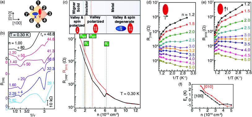
Our material platform is a high-quality 2DES confined to a 21-nm-wide AlAs quantum well Shayegan.AlAs.Review.2006 ; Lay.APL.1993 ; Depoortere.APL.2002 ; Chung.PRM.2018 ; SM . The 2D electrons in the AlAs well occupy two in-plane conduction-band valleys with longitudinal and transverse effective masses , and , leading to an effective in-plane Shayegan.AlAs.Review.2006 ; Lay.APL.1993 ; Depoortere.APL.2002 ; Chung.PRM.2018 ; SM . Via applying uniaxial strain along the [100] direction we transfer all the electrons to the valley whose longer Fermi wavevector axis is along the direction Shayegan.AlAs.Review.2006 ; we refer to this as the Y valley, see Fig. 1(a). As discussed below, this single-valley occupancy can also be achieved, in the absence of uniaxial strain, by tuning to very small values; is controlled in situ by applying voltage to a back gate. The exceptionally high quality of our 2DES can be inferred from Fig. 1(b) which shows magnetoresistance traces measured along [100] as a function of the perpendicular magnetic field () for several ranging from to , in units of cm-2 which we use throughout this paper. We plot the data as a function of so that the quantum Hall states line up for the different traces; is the Landau level filling factor. The traces exhibit clear minima at down to ( footnote.mass ), indicating the presence of fractional quantum Hall states and attesting to the very high sample quality.
Figure 1(c), which presents the sample resistance along [100] and [010], provides an overview of the different transitions and phases observed in our sample as is lowered. Here there is no uniaxial strain applied so that the two in-plane valleys (X and Y), with their major axes along [100] and [010], are equally occupied at high densities; and are essentially equal and the 2DES is isotropic. As is lowered below (), all the electrons suddenly transfer to the Y valley, leading to (note that the electrons in the Y valley have a larger effective mass along [010] compared to [100]). This abrupt, spontaneous valley-polarization, which is akin to Bloch spin ferromagnetism transition, has been discussed in detail elsewhere Hossain.valley ; see also Ahn.Das.Sarma.Valley.cond.mat.2021 . At lower densities, when (), the 2DES turns insulating as signaled by the temperature dependence of and at low temperatures; see Figs. 1(d,e). Note in Fig. 2(d) that near this transition to an insulating phase, we observe a “kink” in resistance vs. traces. At even lower densities, (), the 2DES makes yet another transition to a fully-spin-polarized state Hossain.Spin.Bloch.2020 . Finally, at (), the 2DES becomes highly insulating while still maintaining its anisotropic transport coefficients, and develops a strongly nonlinear I-V characteristic at low temperatures footnote.kink . This phase is the focus of our report here.
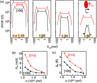
The highlight of our study is presented in Fig. 2(a) where we show the differential resistance along [100] and [010] vs. the dc bias voltage () at very low densities. For Fig. 2 data, as well as in Fig. 3, the 2D electrons occupy only the Y valley. We use log-log plots to cover several orders of magnitude in and . The data in Fig. 2(a) show nonlinear - behavior, with clear threshold voltages () that are larger along [010] compared to [100] (for a given density) heating . We attribute these nonlinearities to the formation of a WS pinned by the ubiquitous disorder potential. Similar nonlinearities at small biases have been observed in previous studies of dilute GaAs 2D holes at Yoon.PRL.1999 , and at very small Landau level fillings in the extreme quantum limit Goldman.PRL.1990 ; Li.Sajoto.PRL.1991 , which also concluded that the nonlinearity in - was a signature of the depinning of a WS. The conclusion for high- data has been further corroborated by numerous experimental studies at very small Landau level fillings, including transport Jiang.PRL.1990 , noise Li.Sajoto.PRL.1991 , magneto-optics Buhmann.PRL.1991 , microwave Andrei.PRL.1988 ; Chen.Nature.Phys.2006 , nuclear magnetic resonance Tiemann.Nat.Phys.2014 , tunneling Jang.Nat.Phys.2016 , geometric resonance Deng.PRL.2016 , and capacitance Deng.PRL.2019 measurements. Therefore, it is likely that in our 2DES, too, the nonlinear I-V signals the formation of a pinned WS at (). Below we elaborate on several important features of the nonlinearities in Fig. 2(a), and argue that they are consistent with an interpretation of our data in terms of a disordered, anisotropic WS.
A key observation in our data is that the magnitude of the threshold electric field () is consistent with the expected depinning of a 2D WS Yoon.PRL.1999 . For example, Chui Chui.PLA.1993 proposed a model in which the WS is weakly pinned by the potential of the remote ionized dopants, and transport takes place through the creation of dislocation pairs and quantum tunneling. In this model, it is estimated that:
| (1) |
where is the density of remote ionized impurities, , and is the spacer-layer thickness. Using relevant and reasonable parameters for our sample (, nm, , and cm-2 Footnote.A ), we estimate V/m. Given that the distance between voltage contacts in our sample [e.g., contacts 2 and 8 in Fig. 1(a)] is mm, V/m corresponds to mV; this is of the order of we observe in our experiments [see Fig. 2(b)]. Given the uncertainty in the value of , we believe our data are consistent with the model of Ref. Chui.PLA.1993 for a pinned WS.
A related implication of Fig. 2 data is the WC pinning energy that can be deduced from the measured Yoon.PRL.1999 . In Fig. 2(c) we plot, as a function of , the values of deduced from the Vth data of Fig. 2(b). Note that Eq. (1) and the above expression for imply that both Vth and should increase as the density is lowered. This behavior is seen qualitatively in Figs. 2(b,c). Moreover, the magnitude of should be comparable to the activation energies extracted from the Arrhenius plots in Fig. 1(f), and this is indeed true, as both sets of data yield energies of a few K.
The Vth data can be used to also extract an approximate size for the WS domain: Li.Sajoto.PRL.1991 . This expression is based on a theory by Fukuyama and Lee Fukuyama.PRB.1978 , and uses the 2D WS shear modulus calculated by Bonsall and Maradudin Bonsall.PRB.1977 . Evaluating this expression for our data at , where V/m [see Fig. 2(b)], we find m2, implying that a typical WS domain contains electrons. This is admittedly not a very large domain, but is plausible, given the amount of disorder in our sample. Note also that, in this model, the anisotropy of implies that the WS domains are anisotropic too, with the domain size along [010] being larger than along [100].
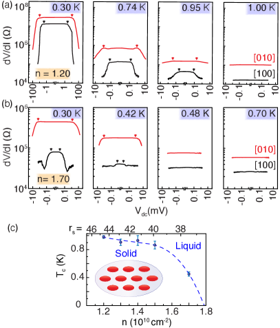
Data of Fig. 3 illustrate another aspect of our 2DES. In Figs. 3(a,b) we show the temperature dependence of nonlinear along [100] and [010] at two different densities, and 1.70. The data indicate that, for a given and direction, moves to smaller values as is raised, and the nonlinearity disappears above a critical temperature . We interpret this disappearance to signal the thermal melting of the WS. As seen in Fig. 3(a), at appears to be between 0.95 K and 1.00 K. Note that the data along [100] and [010] exhibit a similar temperature dependence, implying the same along both directions. When we raise the density, decreases. For example, at , the nonlinearity disappears for K [Fig. 3(b)]. Figure 3(c) summarizes the measured as a function of . As we raise the density, up to , decreases only slightly. However, drops rapidly at higher , implying a quantum melting of the WS at .
The critical temperatures we summarize in Fig. 3(c) are about an order of magnitude larger than the melting temperatures theoretically estimated for an ideal (zero-disorder) quantum WS with parameters similar to our 2DES [see, e.g. Fig. 2(a) of Ref. Das.Sarma.PRB.2003 for GaAs 2D holes]. Also, in our sample the Fermi energy at the lowest densities is small and becomes comparable to the measurement temperatures; this implies that our 2DES approaches the classical limit. It is likely that pinning by the impurities at very low densities is what leads to the much larger melting temperatures in our sample. Indeed, recent theoretical studies, partly motivated by our results, indicate that the effective melting temperature of a WS in the presence of disorder can be significantly enhanced relative to the pristine case as the disordered WS becomes fragmented and localized by the disorder potential VuDasSarma.cond.mat.2021 ; Shklovskii.Unpublished.2021 . Moreover, in a system with disorder, the 2DES eventually attains an Anderson localized state in the limit of extremely small densities because the disorder potential would dominate over the ever-decreasing Coulomb repulsion energy. We note that in Fig. 3(c) are comparable to the melting temperatures reported for the magnetic-field-induced WS phases of dilute 2DESs in GaAs Goldman.PRL.1990 ; Chen.Nature.Phys.2006 ; Deng.PRL.2019 and AlAs KAVR.PRR.2021 , and 2D holes in GaAs Ma.PRL.2020 . They are much smaller than those recently quoted for the zero-field WS phases in MoSe2 Zhou.Nature.2021 ; Smole.Nature.2021 , but much larger than in ZnO Falson.arxiv.2021 .
We close by making several comments concerning the anisotropy observed in our data. First, Fig. 1(b) data show that the transport anisotropy persists in the entire low-density range once all the electrons are transferred to the Y valley (below ). This includes the high densities (e.g., ), when the 2DES is in a “metallic” state, and also deep into the insulating phases at very low densities. Second, for the onset of drops in vs. also show an anisotropy, with along [010] being larger compared to [100] (Figs. 2 and 3). These features are very likely related to the anisotropic effective mass in our 2DES. For a 2DES like ours, with a large effective mass along the direction () and a small mass along (), the electron charge distribution has an elliptical shape which is rotated by 90o with respect to the shape of the Fermi sea/contour [see Fig. 3(c) inset]. Such a charge distribution would imply that transport along would be harder compared to as the electrons are more localized (smaller Bohr radius) and have less overlap along . This is consistent with our observations. Now, theory Wan.PRB.2002 suggests that in a 2DES with an anisotropic effective mass, the WS is distorted from its conventional, triangular lattice, and has a shape schematically shown in Fig. 3(c) inset. Note that, compared to the conventional triangular lattice, here the lattice is stretched along the axis. (The stretch along the axis of the smaller mass reduces the longitudinal energy of lattice vibrations, thus lowering the ground state energy Wan.PRB.2002 ). It then appears that the transport and anisotropies would depend on the competition between the anisotropies of the electron charge distribution and the WS lattice, e.g., a very large elongation of the lattice might eventually lead to a reversal of the transport anisotropy, with resistance and along exceeding those along . We do not observe such reversal of anisotropies, suggesting that the transport anisotropy in our 2DES is controlled by the electron charge distribution anisotropy.
Acknowledgements.
We acknowledge support through the U.S. Department of Energy Basic Energy Sciences (Grant No. DEFG02-00-ER45841) for measurements, and the National Science Foundation (Grants No. DMR 2104771, No. ECCS 1906253, DMR 1709076, and MRSEC DMR 2011750), the Eric and Wendy Schmidt Transformative Technology Fund, and the Gordon and Betty Moore Foundation’s EPiQS Initiative (Grant No. GBMF9615 to L. N. P.) for sample fabrication and characterization. We also thank J. K. Jain, S. Das Sarma, L. W. Engel, D. A. Huse, M. A. Mueed, and B. Shklovskii for illuminating discussions.References
- (1) D. C. Tsui, H. L. Stormer, and A. C. Gossard, Two-dimensional magnetotransport in the extreme quantum limit, Phys. Rev. Lett. 48, 1559 (1982).
- (2) E. Wigner, On the interaction of electrons in metals, Phys. Rev. 46, 1002 (1934).
- (3) E. Y. Andrei, G. Deville, D. C. Glattli, F. I. B. Williams, E. Paris, and B. Etienne, Observation of a Magnetically Induced Wigner Solid, Phys. Rev. Lett. 60, 2765 (1988).
- (4) H. W. Jiang, R. L. Willett, H. L. Stormer, D. C. Tsui, L. N. Pfeiffer, and K. W. West, Quantum liquid versus electron solid around Landau-level filling, Phys. Rev. Lett. 65, 633 (1990).
- (5) V. J. Goldman, M. Santos, M. Shayegan, and J. E. Cunningham, Evidence for two-dimentional quantum Wigner crystal, Phys. Rev. Lett. 65, 2189 (1990).
- (6) Y. P. Li, T. Sajoto, L. W. Engel, D. C. Tsui, and M. Shayegan, M. Low-frequency noise in the reentrant insulating phase around the fractional quantum Hall liquid, Phys. Rev. Lett. 67, 1630 (1991).
- (7) H. Buhmann, W. Joss, K. von Klitzing, I. V. Kukushkin, A. S. Plaut, G. Martinez, K. Ploog, and V. B. Timofeev, Novel magneto-optical behavior in the Wigner-solid regime, Phys. Rev. Lett. 66, 926 (1991).
- (8) M. B. Santos, Y. W. Suen, M. Shayegan, Y. P. Li, L. W. Engel, and D. C. Tsui, Observation of a reentrant insulating phase near the 1/3 fractional quantum Hall liquid in a two-dimensional hole system, Phys. Rev. Lett. 68, 1188 (1992).
- (9) M. B. Santos, J. Jo, Y. W. Suen, L. W. Engel, and M. Shayegan, Effect of Landau-level mixing on quantum-liquid and solid states of two-dimensional hole systems, Phys. Rev. B 46, 13639(R) (1992).
- (10) J. Yoon, C. C. Li, D. Shahar, D. C. Tsui, and M. Shayegan, Wigner Crystallization and Metal-Insulator Transition of Two-Dimensional Holes in GaAs at , Phys. Rev. Lett. 82, 1744 (1999).
- (11) Y. P. Chen, G. Sambandamurthy, Z. H. Wang, R. M. Lewis, L. W. Engel, D. C. Tsui, P. D. Ye, L. N. Pfeiffer, and K. W. West, Melting of a 2D quantum electron solid in high magnetic field, Nat. Phys. 2, 452 (2006).
- (12) L. Tiemann, T. D. Rhone, N. Shibata, and K. Muraki, NMR profiling of quantum electron solids in high magnetic fields, Nat. Phys. 10, 648 (2014).
- (13) H. Deng, Y. Liu, I. Jo, L. N. Pfeiffer, K. W. West, K. W. Baldwin, and M. Shayegan, Commensurability Oscillations of Composite Fermions Induced by the Periodic Potential of a Wigner Crystal,Phys. Rev. Lett. 117, 096601 (2016).
- (14) J. Jang, B. M. Hunt, L. N. Pfeiffer, K. W. West, and R. C. Ashoori, Sharp tunnelling resonance from the vibrations of an electronic Wigner crystal, Nat. Phys. 13, 340 (2017).
- (15) H. Deng, L. N. Pfeiffer, K. W. West, K. W. Baldwin, L. W. Engel, and M. Shayegan, Probing the Melting of a Two-Dimensional Quantum Wigner Crystal via its Screening Efficiency, Phys. Rev. Lett. 122, 116601 (2019).
- (16) M. S. Hossain, M. K. Ma, K. A. Villegas Rosales, Y. J. Chung, L. N. Pfeiffer, K. W. West, K. W. Baldwin, and M. Shayegan, Observation of spontaneous ferromagnetism in a two-dimensional electron system, Proc. National Acad. Sci. 117, 32244 (2020).
- (17) M. K. Ma, K. A. Villegas Rosales, H. Deng, Y. J. Chung, L. N. Pfeiffer, K. W. West, K. W. Baldwin, R. Winkler, and M. Shayegan, Thermal and Quantum Melting Phase Diagrams for a Magnetic-Field-Induced Wigner Solid, Phys. Rev. Lett. 125, 036601 (2020).
- (18) K. A. Villegas Rosales, S. K. Singh, Meng K. Ma, Md. Shafayat Hossain, Y. J. Chung, L. N. Pfeiffer, K. W. West, K. W. Baldwin, and M. Shayegan, Competition between fractional quantum Hall liquid and Wigner solid at small fillings: Role of layer thickness and Landau level mixing, Phys. Rev. Research 3, 013181 (2021).
- (19) Y. Zhou, J. Sung, E. Brutschea, I. Esterlis, Y. Wang, G. Scuri, R. J. Gelly, H. Heo, T. Taniguchi, K. Watanabe, G. Zaránd, M. D. Lukin, P. Kim, E. Demler, and H. Park, Bilayer Wigner crystals in a transition metal dichalcogenide heterostructure, Nature 595, 48 (2021).
- (20) T. Smoleński, P. E. Dolgirev, C. Kuhlenkamp, A. Popert, Y. Shimazaki, P. Back, X. Lu, M. Kroner, Kenji Watanabe, T. Taniguchi, I. Esterlis, E. Demler, and Ataç Imamoğlu, Signatures of Wigner crystal of electrons in a monolayer semiconductor, Nature 595, 53 (2021)
- (21) J. Falson, I. Sodemann, B. Skinner, D. Tabrea, Y. Kozuka, A. Tsukazaki, M. Kawasaki, K. von Klitzing, and J. H. Smet, Competing correlated states around the zero field Wigner crystallization transition of electrons in two-dimensions, Nature Materials 21, 311 (2022).
- (22) F. Bloch, Bemerkung zur Elektronentheorie des Ferromagnetismus und der elektrischen Leitfähigkeit, Z. Phys. 57, 545 (1929).
- (23) B. Tanatar and D. M. Ceperley, Ground state of the two-dimensional electron gas, Phys. Rev. B 39, 5005 (1989).
- (24) C. Attaccalite, S. Moroni, P. Gori-Giorgi, and G. B. Bachelet, Correlation energy and spin polarization in the 2D electron gas, Phys. Rev. Lett. 88, 256601 (2002).
- (25) N. D. Drummond and R. J. Needs, Phase Diagram of the Low-Density Two-Dimensional Homogeneous Electron Gas, Phys. Rev. Lett. 102, 126402 (2009).
- (26) A. L. Sharpe, E. J. Fox, A. W. Barnard, , J. Finney, K.Watanabe, T. Taniguchi, M. A. Kastner, and D. Goldhaber-Gordon, Emergent ferromagnetism near three-quarters filling in twisted bilayer graphene, Science 365, 605 (2019).
- (27) J. G. Roch, D. Miserev, G. Froehlicher, N. Leisgang, L. Sponfeldner, K. Watanabe, T. Taniguchi, J. Klinovaja, Daniel Loss, and Richard J. Warburton, First-Order Magnetic Phase Transition of Mobile Electrons in Monolayer MoS2, Phys. Rev. Lett. 124, 187602 (2020).
- (28) H. Polshyn, J. Zhu, M. A. Kumar, Y. Zhang, F. Yang, C. L. Tschirhart, M. Serlin, K. Watanabe, T. Taniguchi, A. H. MacDonald, and A. F. Young, Electrical switching of magnetic order in an orbital Chern insulator, Nature 588, 66 (2020).
- (29) Md. S. Hossain, T. Zhao, S. Pu, M. A. Mueed, M. K. Ma, K. A. V. Rosales, Y. J. Chung, L. N. Pfeiffer, K. W. West, K. W. Baldwin, J. K. Jain, M. Shayegan, Bloch ferromagnetism of composite fermions, Nat. Phys. 17, 48 (2021) (2021).
- (30) X. Wan and R. N. Bhatt, Two-dimensional Wigner crystal in anisotropic semiconductors, Phys. Rev. B 65, 233209 (2002).
- (31) C. Zhou and R. N. Bhatt, Zero temperature magnetic phase diagram of Wigner crystal in anisotropic two-dimensional electron systems, Physica B: Condensed Matter 403, 1547 (2008).
- (32) J. Xia, J. P. Eisenstein, L. N. Pfeiffer, and K. W. West, Evidence for a fractionally quantized Hall state with anisotropic longitudinal transport, Nat. Phys. 7, 845 (2011).
- (33) T. Gokmen, M. Padmanabhan, and M. Shayegan, Transference of transport anisotropy to composite fermions, Nat. Phys. 6, 621 (2010).
- (34) M. Mulligan, C. Nayak, and S. Kachru, Effective field theory of fractional quantized Hall nematics, Phys. Rev. B 84, 195124 (2011).
- (35) B. Yang, Z. Papić, E. H. Rezayi, R. N. Bhatt, and F. D. M. Haldane, Band mass anisotropy and the intrinsic metric of fractional quantum Hall systems, Phys. Rev. B 85, 165318 (2012).
- (36) Y. Liu, S. Hasdemir, M. Shayegan, L. N. Pfeiffer, K. W. West, and K. W. Baldwin, Evidence for a fractional quantum Hall nematic state in parallel magnetic fields, Phys. Rev. B 88, 035307 (2013).
- (37) D. Kamburov, Yang Liu, M. Shayegan, L. N. Pfeiffer, K. W. West, and K. W. Baldwin, Composite Fermions with Tunable Fermi Contour Anisotropy, Phys. Rev. Lett. 110, 206801 (2013).
- (38) D. Kamburov, M. A. Mueed, M. Shayegan, L. N. Pfeiffer, K. W. West, K. W. Baldwin, J. J. D. Lee, and R. Winkler, Fermi contour anisotropy of GaAs electron-flux composite fermions in parallel magnetic fields, Phys. Rev. B 89, 085304 (2014).
- (39) Y. Liu, S. Hasdemir, L. N. Pfeiffer, K. W. West, K. W. Baldwin, and M. Shayegan, Observation of an Anisotropic Wigner Crystal, Phys. Rev. Lett. 117, 106802 (2016).
- (40) B. E. Feldman, M. T. Randeria, A. Gyenis, F. Wu, H. Ji, R. J. Cava, A. H. MacDonald, and A. Yazdani, Observation of a nematic quantum Hall liquid on the surface of bismuth, Science 354, 316 (2016).
- (41) I. Jo, K. A. Villegas Rosales, M. A. Mueed, L. N. Pfeiffer, K. W. West, K. W. Baldwin, R. Winkler, M. Padmanabhan, and M. Shayegan, Transference of Fermi contour anisotropy to composite fermions, Phys. Rev. Lett. 119, 016402 (2017).
- (42) Md. S. Hossain, M.K. Ma, Y. J. Chung, L. N. Pfeiffer, K. W. West, K. W. Baldwin, and M. Shayegan, Unconventional Anisotropic Even-Denominator Fractional Quantum Hall State in a System with Mass Anisotropy, Phys. Rev. Lett. 121, 256601 (2018).
- (43) M. S. Hossain, M. K. Ma, K. A. Villegas Rosales, Y. J. Chung, L. N. Pfeiffer, K. W. West, K. W. Baldwin, and M. Shayegan, Spontaneous valley polarization of itinerant electrons, Phys. Rev. Lett. 127, 116601 (2021).
- (44) An anisotropic WS at high magnetic fields has been reported Liu.PRL.2016 . However, this state is observed under very specific and unusual conditions, namely in a 2D hole system confined to a wide GaAs quantum well, at a relatively large density and with a bilayer-like charge distribution, and only near the crossing of the lowest two Landau levels induced by tilting the sample in the magnetic field.
- (45) T. Sajoto, Y. W. Suen, L. W. Engel, M. B. Santos, and M. Shayegan, Fractional quantum Hall effect in very-low-density GaAs/AlxGa1-xAs heterostructures, Phys. Rev. B 41, 8449 (1990).
- (46) J. Zhu, H. L. Stormer, L. N. Pfeiffer, K. W. Baldwin, and K. W. West, Spin susceptibility of an ultra-low-density two-dimensional electron system, Phys. Rev. Lett. 90, 056805 (2003).
- (47) M. Shayegan, E. P. De Poortere, O. Gunawan, Y. P. Shkolnikov, E. Tutuc, and K. Vakili, Two-dimensional electrons occupying multiple valleys in AlAs, Phys. Stat. Sol. (b) 243, 3629 (2006).
- (48) T. S. Lay, J. J. Heremans, Y. W. Suen, M. B. Santos, K. Hirakawa, M. Shayegan, and A. Zrenner, High‐quality two‐dimensional electron system confined in an AlAs quantum well, Applied Physics Letters 62, 3120 (1993).
- (49) E. P. De Poortere, Y. P. Shkolnikov, E. Tutuc, S. J. Papadakis, and M. Shayegan, Enhanced electron mobility and high order fractional quantum Hall states in AlAs quantum wells, Appl. Phys. Lett. 80, 1583 (2002).
- (50) Y. J. Chung, K. A. Villegas Rosales, H. Deng, K. W. Baldwin, K. W. West, M. Shayegan, and L. N. Pfeiffer, Multivalley two-dimensional electron system in an AlAs quantum well with mobility exceeding cm2/Vs, Phys. Rev. Materials 2, 071001(R) (2018).
- (51) See Supplemental Material for a discussion on our material platform and additional data which includes Refs. Williams.PRL.1991 ; Goldys.PRB.1992 ; Zhao.PRL.2018 ; Kim.PNAS.2021 ; Shahar.1997 .
- (52) F. I. B. Williams, P. A. Wright, R. G. Clark, E. Y. Andrei, G. Deville, D. C. Glattli, O. Probst, B. Etienne, C. Dorin, C. T. Foxon, and J. J. Harris, Conduction Threshold and Pinning Frequency of Magnetically Induced Wigner Solid, Phys. Rev. Lett. 66, 3285 (1991).
- (53) E. M. Goldys, S. A. Brown, R. B. Dunford, A. G. Davies, R. Newbury, R. G. Clark, P. E. Simmonds, J. J. Harris, and C. T. Foxon, Magneto-optical probe of two-dimensional electron liquid and solid phases, Phys. Rev. B 46, 7957 (1992).
- (54) J. Zhao, Y. Zhang, and J. K. Jain, Crystallization in the fractional quantum Hall regime induced by Landau-level mixing, Phys. Rev. Lett. 121, 116802 (2018).
- (55) Kyung-Su Kim, Steven A. Kivelson, Discovery of an insulating ferromagnetic phase of electrons in two dimensions, Proc. National Acad. Sci. 118, e2023964118 (2021).
- (56) D. Shahar, D. C. Tsui, M. Shayegan, J. E. Cunningham, E. Shimshoni, S. L. Sondhi, On the nature of the Hall insulator. Solid State Commun. 102, 817 (1997).
- (57) To calculate values, we use the effective in-plane band mass which is equal to . When electrons occupy a single valley, one can define along [100] and [010] separately. This would lead to an anisotropic . For example, when electrons occupy only the Y valley, and . Therefore, . and are related to the values that we used as follows: .
- (58) S. Ahn and S. D. Sarma, Valley polarization transition in a two-dimensional electron gas, arXiv:2110.09528 (2021).
- (59) Note in Fig. 1(c) that near , and show a second “kink” towards higher resistances at lower temperatures.
- (60) Note that the power dissipated in the sample is much smaller than the cooling power of the cryostat. Also, Joule self-heating in the 2DES is not responsible for the nonlinearities we report: At a given density and temperature, the power required to achieve the same change in the differential resistance is more than an order of magnitude different along the two directions. We therefore conclude that the effect of heating is negligible in our measurements.
- (61) S. T. Chui, Depinning, defect creation and quantum tunnelling, Phys. Lett. A 180, 149 (1993).
- (62) The parameter is not precisely known for modulation-doped samples; it is typically smaller than the concentration of the -doping layer but larger than the 2DES density in the quantum well.
- (63) H. Fukuyama and P. A. Lee, Dynamics of the charge-density wave. I. Impurity pinning in a single chain, Phys. Rev. B 17, 535 (1978).
- (64) L. Bonsall and A. A. Maradudin, Some static and dynamical properties of a two-dimensional Wigner crystal, Phys. Rev. B 15, 1959 (1977).
- (65) S. Das Sarma and E. H. Hwang, Low-density finite-temperature apparent insulating phase in two-dimensional semiconductor systems, Phys. Rev. B 68, 195315 (2003).
- (66) D. D. Vu and S. D. Sarma, Thermal melting of a quantum electron solid in the presence of strong disorder: Anderson versus Wigner, arXiv:2110.06229 (2021).
- (67) B. I. Shklovskii, unpublished.