Anomalous Fano factor as a signature of Bogoliubov Fermi surfaces
Abstract
Noise spectroscopy is a key technique to investigate the nature and dynamics of charge carriers in superconductors. The recently discovered superconducting hybrids with Bogoliubov Fermi surfaces exhibit a particularly intriguing and rich charge dynamics, as their charge carriers consist of both Cooper pairs and an extensive number of Bogoliubov quasiparticles. Motivated by this, we compute the noise spectra of Bogoliubov Fermi surfaces and identify their key signatures in the differential conductance and the Fano factor. Specifically, we consider a semiconductor/superconductor hybrid device with an in-plane magnetic field, which exhibits several Bogoliubov Fermi surfaces. The number and orientation of the Bogoliubov Fermi surfaces in this device can be readily controlled by the applied magnetic field, which in turn alters the noise signal. In particular, we find that the Fano factor exhibits a reduced value, substantially lower than two, whenever the charge dynamics is governed by a large number of Bogoliubov quasiparticles. Using experimentally relevant parameters, we make a number of specific predictions for the noise spectra, that can be used as direct evidence of Bogoliubov Fermi surfaces. In particular, we find that the Fano factor as a function of magnetic field and spin-orbit coupling exhibits characteristic discontinuities at the transition lines that separate phases with different number of Bogoliubov Fermi surfaces.
I Introduction
Since the discovery of unconventional superconductors in the 1980s Bednorz and Muller (1986); Stewart (1984); Keimer et al. (2015), the study of low-energy Bogoliubov quasiparticles (BQPs) has been an important research topic with both fundamental and applied interest Schrieffer and Brooks (2007). Usually, unconventional superconductors exhibit only point nodes or line nodes in their pairing gap, with dimension strictly smaller than the normal-state Fermi surface, due to the loss of condensation energy. However, recent findings have shown that there can also exist two-dimensional nodes in the superconducting gap, which form a Fermi surface of BQPs whose dimension is equal to the normal-state Fermi surface. For instance, Bogoliubov Fermi surfaces (BFSs) can exist in multi-band superconductors with broken time-reversal symmetry Volovik (1989); Agterberg et al. (2017); Timm et al. (2017); Brydon et al. (2018); Menke et al. (2019), in nodal superconductors with external Zeeman potentials Yang and Sondhi (1998); Gubankova et al. (2005); Setty et al. (2020), and in superconductors carrying large supercurrents Fulde (1965); Zhu et al. (2021). In addition, BFSs can be created in superconducting hybrids, such as semiconductor-superconductor heterostructures with strong spin-orbit coupling (SOC) and an external Zeeman field Phan et al. (2022); Yuan and Fu (2018). The recent experimental observation of BFSs in superconductor hybrids Phan et al. (2022); Zhu et al. (2021) has further stimulated this field.
The presence of BFSs with their extensive number of BQPs leads to a large density of states at zero energy, which can be detected by a number of experimental probes. For example, the large zero-energy density of states can be directly observed in tunneling conductance Setty et al. (2020); Lapp et al. (2020) and specific heat Setty et al. (2020); Lapp et al. (2020), and moreover leads to characteristic signatures in quasiparticle interference patterns Zhu et al. (2021). While these experimental probes detect the presence of zero-energy quasiparticles, they do not provide information about their nature and dynamics. This is where noise spectroscopy comes into play, which can measure the fundamental charge of the quasiparticles as well as their dynamics. For example, the current-noise ratio (i.e., Fano factor) in the tunneling limit of a fully gapped superconductor is twice as large as in the normal state de Jong and Beenakker (1994); Anantram and Datta (1996), indicating that the charge carriers are Cooper pairs composed of two electrons. However, in systems with BFSs, where the charge carriers consist of both Cooper pairs and BQPs, the Fano factor is expected to be smaller than two, since the effective charge of the BQPs is substantially smaller than that of Cooper pairs. Hence, noise spectroscopy can give valuable information about the presence of BFSs and can tell us to which degree BQPs contribute to charge transport.
Motivated by these considerations, we investigate in this Letter the Fano factor of a semiconductor/superconductor hybrid device which exhibits BFSs that can be controlled by an external magnetic field. After defining the model Hamiltonian of the considered device (Sec. II), we determine in Sec. III the regions in parameter space of SOC and field strength, where BFSs exist. Interestingly, we find that with increasing field strength our device can be tuned through two phase transitions, where the number of BFSs increases from zero to two to four (Fig. 2). In Sec. IV we present our results on the differential conduction and noise spectroscopy. We observe that both the differential conductance and the Fano factor exhibit characteristic discontinuities at the phase transition lines. In the tunneling limit the value of the Fano factor reduces from two to about one, indicating that a substantial part of the charge is carried by BQPs rather than Cooper pairs. These results provide key fingerprints for the experimental identification of BFSs in the considered device.
II Model definition
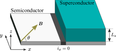
We consider a thin-film semiconductor/superconductor hybrid device with an external magnetic field applied in-plane, as illustrated in Fig. 1. The superconductor is assumed to be of conventional nature with spin-singlet -wave pairing, while the semiconductor is non-centrosymmetric with a substantial Rashba SOC, as realized in, e.g., Al/InAs heterostructures Phan et al. (2022); Kjaergaard et al. (2016). The semiconductor is separated into two regions by a potential barrier at , whose transparency can be controlled experimentally by applying gate voltages. Due to proximity to the parent superconductor, the semiconductor at acquires an induced -wave pair potential Phan et al. (2022); Kjaergaard et al. (2016); Suominen et al. (2017); Kjaergaard et al. (2017); Mayer et al. (2019). As a result, the hybrid device realizes an effective two-dimensional NS junction with tunable potential barrier and in-plane field. As we will see, the high tunability of the device allows us to study the conductance and noise signals for different BFSs configurations and junction transparencies.
Mathematically, we describe the considered device by a Bogoliubov-de Gennes (BdG) Hamiltonian on a three-dimensional cubic lattice with lattice sites labelled by , where the three lattice vectors , , and are assumed to have unit length . We can separate the BdG Hamiltonian into three parts, , representing the semiconductor, the superconductor, and the coupling between them, respectively. The Hamiltonian of the two-dimensional semiconductor at is given by
| (1) |
where are the three Pauli matrices in spin space, and denotes the unit matrix. Here, represents a spinor composed of operators () which annihilate (create) electrons with spin at sites within the semiconductor. denotes the nearest-neighbor hopping amplitude and is the onsite energy, with the chemical potential. The strength of the Rashba SOC and the potential barrier at are denoted by and , respectively. The in-plane magnetic field induces a Zeeman potential of strength , where and deonte the Bohr magneton and the -factor of the semiconductor, respectively.
The Hamiltonian of the three-dimensional superconductor, located at and , reads
| (2) |
where is a spinor composed of operators () which annihilate (create) electrons with spin at sites within the superconductor. denotes the hopping amplitude in the superconductor, represents the spin-singlet -wave pair potential, and is the onsite energy, with the chemical potential. The Zeeman potential in the superconductor is given by , with strength and -factor . Finally, the coupling between the semiconductor and the superconductor is given by
| (3) |
with amplitude . This coupling induces a finite superconducting pair potential in the semiconductor segment , which we compute using lattice Greens function techniques Lee and Fisher (1981); Ando (1991).
For the numerical calculations, we set the parameters to , , , , and . In addition, we fix the ratio of the -factors to and express the strength of the potential barrier by the normalized value , with the Fermi momentum of the semiconductor. We note that the choice of and corresponds to the experimentally relevant regime, as observed, e.g., in Al/InAs heterostructures Phan et al. (2022); Kjaergaard et al. (2016). In the following, we calculate the differential conductance and the Fano factor as a function of junction transparency , SOC strength , and Zeeman field , for different field orientations . We note that with this choice is given by .
III Phase diagram
Before calculating the conductance and noise spectra, we first determine the parameter regions where BFSs emerge in the considered device. For this purpose, we remove the semiconductor segment and apply periodic boundary conditions in both - and -directions. By Fourier transforming the spinors and , as and , the BdG Hamiltonian is simplified to
| (4) |
where is given in the Supplemental Material (SM) sm_ and , with and . In the presence of time-reversal symmetry (TRS) and inversion, the emergence of BFSs can be detected by use of a Pfaffian index, as discussed in Refs. [Agterberg et al., 2017; Timm et al., 2017; Brydon et al., 2018; Zhao et al., 2016]. In the case of Hamiltonian (4), however, the Pfaffian index is no longer well defined, since TRS and inversion are broken by the magnetic field and Rashba SOC, respectively. Instead, we introduce for a given wave vector of the two-dimensional Brillouin zone (BZ) a determinant index , which can be used even in the absence of TRS and inversion. It is defined by
| (5) |
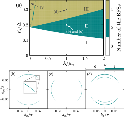
where is the (arbitrarily chosen) origin of the BZ. We note that is defined modulo , with indicating that the energy gap of the BdG Hamiltonian closes at a momentum between and the BZ origin . Hence, two-dimensional regions with in the BZ are bounded by a gapless line that forms a BFS. This is demonstrated in Figs. 2(b)-2(d), where we plot in the two-dimensional BZ for three different parameter choices indicated in Fig. 2(a), namely , , and , respectively. We observe pairs of thin banana-shaped regions where , which are bounded by BFSs.
The orientation of these BFSs is controlled by the field angle . That is, with increasing the BFSs rotate counterclockwise from the 12’o clock and 6’o clock positions for [Fig. 2(b)] to the 3’o clock and 9’o clock positions for [Fig. 2(c)]. The length of the banana-shaped BFSs can be tuned by the Zeeman field . I.e., with increasing the BFSs become longer and longer. For sufficiently large a phase transition point is reached, at which two more point-like BFSs appear, which are inflated into banana shapes, by further increasing . As a function of Zeeman field and SOC we observe three regions that exhibit BFSs [phases II, III, and IV in Fig. 2(a)]. Phase II has two BFSs, while phases III and IV have four BFSs. We note that phases III and IV are separated by a thin line, where the two pairs of BFSs touch each other, cf. dashed line in Fig. 2(a) and Figs. S1(b) and S1(e) in the SM. In the next section we discuss the conductance and noise spectra of phases I, II, and III, and the transitions between them. The transition between phases III and IV is investigated in the SM sm_ .
IV Differential conductance and noise spectroscopy
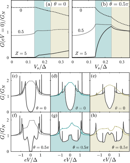
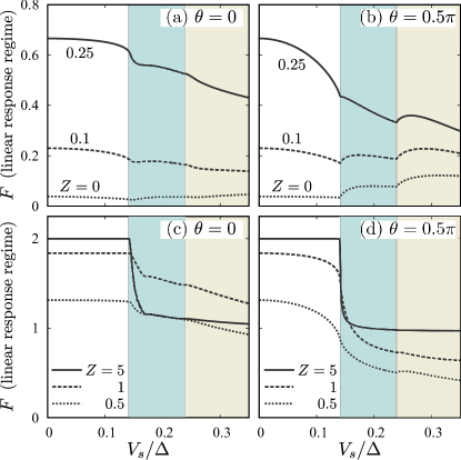
Let us now turn to the transport properties, which we use to characterize the different phases I, II, and III of Fig. 2. In order to compute the differential conductance and the current-noise ratio , we impose periodic boundary conditions in the -direction of the considered device (Fig. 1). For concreteness we fix the value of the Rashba SOC to and study the transport properties as a function of Zeeman field , with . By examining Fig. 2, we find that for , phase I (no BFSs) occurs for , phase II (two BFSs) is realized for , while phase III (four BFSs) exists for . These three phases are marked in Fig. 3 and Fig. 4 by white, green, and grey color, respectively.
We first examine the differential conductance at zero temperature, which we compute within the Blonder–Tinkham–Klapwijk formalism (BTK) Blonder et al. (1982). For this purpose we apply a bias voltage to our device, which injects electrons from . The differential conductance is evaluated by
| (6a) | |||
| (6b) | |||
where for () represents the normal (Andreev) reflection coefficient from an electron with spin to an electron (hole) with spin at momentum and energy . denotes the summation over of the propagating channels. The reflection coefficients are calculated using lattice Green’s function techniques Lee and Fisher (1981); Ando (1991). In the figures we show the normalized differential conductance , which is obtained by dividing by the normal conductance calculated by setting .
In Figs. 3(c)-(h) we show as a function of bias voltage for the three phases of Fig. 2(a) and the field angles [top row, panels (c)-(e)] and [bottom row, panels (f)-(h)]. Figs. 3(a) and 3(b) display at zero bias as a function of Zeeman field for and , respectively. Let us first focus on the tunneling limit with low junction transparency (solid lines). For the tunneling limit we observe in all panels (c)-(h) two peaks symmetrically located around . These double peaks are the coherence peaks of the parent superconductor, which are split by the applied Zeeman field (cf. Fig. S2 of the SM sm_ ). In addition there are smaller peaks (mostly at smaller bias), which originate from the proximity induced superconductivity of the semimetal. Around zero-bias voltage we observe clear signatures of the BFSs, i.e., in the tunneling limit there is residual conductance at zero bias originating from the finite zero-energy density of states of the BFSs. The conductance around zero bias increases with increasing and shows kink singularities at the phase transitions points, where the number of BFSs jumps from zero to two and from two to four (see solid lines in Figs. 3(a) and 3(b)]. Interestingly, the zero-bias conductance is larger for than for . This is due to the fact that for most of the incident electrons (i.e., those with ) cannot couple to the BFSs, while for almost all incident electrons can tunnel into the BFSs [see Figs. 1(b)-(d)].
Also in the ballistic limit with a completely transparent junction () distinct signatures of the BFSs can be observed in around zero bias (dashed lines in Fig. 3). That is, in the absence of BFSs all incident electrons show perfect Andreev reflection yielding , while in the presence of BFSs only parts of the electrons Andreev reflect leading to a suppression of , with . As in the tunneling limit, we observe distinct kink singularities at the transition points that separate phases with different numbers of BFSs [see dashed lines in Figs. 3(a) and 3(b)]. In passing, we note that the conductance spectra (particularly in the ballistic limit ) are not symmetric around zero bias. The reason for this is the broken time-reversal and broken inversion symmetry, as discussed in more detail in the SM sm_ .
Let us now turn to the noise spectra of the BFSs. For this purpose we compute the current-noise ratio (Fano factor) within the linear response regime, i.e., for , where the BFSs show a dominant contribution. The current-noise ratio is given by the ratio between the zero-frequency noise power
| (7) |
and the time averaged current at zero temperature . Here, denotes the deviation of the current at time from the averaged current . Within the linear response regime, the Fano factor at zero bias simplifies to
| (8) |
where the noise power de Jong and Beenakker (1994); Anantram and Datta (1996) is evaluated within the BTK formalism Blonder et al. (1982), as
| (9) |
As before, we compute the reflection coefficients entering in the above formula by use of lattice Greens function techniques Lee and Fisher (1981); Ando (1991).
In Fig. 4 we present the zero-bias Fano factor, Eq. (8), as a function of Zeeman field for six different junction transparencies . The left column [(a) and (c)] corresponds to the field angle , while the right column [(b) and (d)] shows the results for the field angle . The different phases of Fig. 2(a), with different numbers of BFSs, are indicated by the white, green, and grey colors, respectively. In the tunneling limit with low junction transparency the Fano factor gives us information about the fundamental charge of the quasiparticles that tunnel across the junction. In phase I without BFSs (white regions), the Fano factor takes the value of two, since the tunneling current is carried exclusively by Cooper pairs composed of two electrons. In phases II and III, however, which exhibit a large number of BQPs forming BFSs (green and grey regions), the Fano factor decreases to a value substantially lower than two. This indicates that the current is carried by both Cooper pairs and BQPs, which have an effective charge substantially smaller than that of Cooper pairs. Remarkably, if we set the field angle to , such that almost all incident electrons can couple to the BFSs, the Fano factor drops below one [solid line in Fig. 4(c)], implying that almost all of the current is carried by the BQPs.
In the ballistic limit with transparent junction , we can obtain information about the types of scattering processes that occur at the junction barrier. In phase I without BFSs we observe that the Fano factor is almost zero [dotted lines in Figs. 4(a) and 4(b)], as almost all incident electrons undergo Andreev reflection such that the noise power is almost zero. In phases II and III with BFSs, however, the Fano factor increases, indicating that some electrons are transformed into BQPs of the BFSs, while others Andreev reflect. By setting the field angle to , we can maximize the coupling between the lead electrons and the BFS, such that more electrons transmit into the BFSs, thereby increasing the Fano factor [cf. dotted lines in Figs. 4(a) and 4(b)]. As in Fig. 3 we observe distinct kinks in the Fano factor at the transition points that separate the different phases.
V Conclusions
In summary, we have investigated the differential conductance and noise spectroscopy of a NS junction with BFSs. We find that the current-noise ratio (Fano factor) provides key fingerprints of the presence of BFSs (see Fig. 4): In the tunneling limit the Fano factor drops from two to about one, whenever there are BFSs present. In the ballistic limit, on the other hand, the Fano factor jumps from zero to a finite value, due to the presence of BFSs. Moroever, the Fano factor as a function of Zeeman field exhibits kink discontinuities at the transition lines that separate phases with different number of BFSs. We hope that these predictions will help experimentalists to identify the presence of BFSs in their superconducting hybrid devices.
We note that the creation of BFSs in semiconductor/superconductor hybrid devices requires Zeeman fields larger than the proximity-induced pair potential in the semiconductor, but smaller than the critical field of the parent superconductor. This condition is realized for hybrid devices, such as Al/InAs heterostructures Phan et al. (2022); Kjaergaard et al. (2016), where the factor of the semiconductor is large, while the proximity-induced pair potential is small compared to the parent superconductor. While we have focused in this Letter on superconducting hybrids with BFSs, the obtained results are of relevance also to other systems with BFSs, for example, multi-band superconductors with broken time-reversal symmetry Agterberg et al. (2017); Timm et al. (2017); Brydon et al. (2018); Menke et al. (2019).
In closing, we mention several promising directions for future research. First, it would be interesting to investigate other types of junctions, e.g., NSN and SNS junctions, involving superconductors with BFSs, and to determine the signatures of BFSs in the Josephson current. Experimentally, it should be straightforward to fabricate NSN and SNS junctions using existing thin film technology. Second, it would be of interest to study thermal transport properties of BFSs. While conventional superconductors are prefect thermal insulators at low temperature, superconductors with BFSs are expected to show substantial thermal transport carried by the large density of BQPs near zero energy. Third, the interplay between BFSs and Andreev surface bound states (or interface bound states) and its effects on the transport properties would be a worthwhile topic for future research.
Acknowledgements.
The authors thank O. Maistrenko and P. Bonetti for useful discussions. S.I. is supported by the Grant-in-Aid for JSPS Fellows (JSPS KAKENHI Grant No. JP21J00041) and the JSPS Core-to-Core Program (No. JPJSCCA20170002). S.B. thanks the MPI-FKF for financial support.References
- Bednorz and Muller (1986) J. G. Bednorz and K. A. Muller, Z. Phys. B 64, 189 (1986).
- Stewart (1984) G. R. Stewart, Rev. Mod. Phys. 56, 755 (1984).
- Keimer et al. (2015) B. Keimer, S. A. Kivelson, M. R. Norman, S. Uchida, and J. Zaanen, Nature 518, 179 (2015).
- Schrieffer and Brooks (2007) J. R. Schrieffer and J. S. Brooks, Handbook of High Temperature Superconductivity (Springer Science, 2007).
- Volovik (1989) G. E. Volovik, Physics Letters A 142, 282 (1989).
- Agterberg et al. (2017) D. Agterberg, P. Brydon, and C. Timm, Physical Review Letters 118, 127001 (2017).
- Timm et al. (2017) C. Timm, A. P. Schnyder, D. F. Agterberg, and P. M. R. Brydon, Physical Review B 96, 094526 (2017).
- Brydon et al. (2018) P. M. R. Brydon, D. F. Agterberg, H. Menke, and C. Timm, Physical Review B 98, 224509 (2018).
- Menke et al. (2019) H. Menke, C. Timm, and P. M. R. Brydon, Physical Review B 100, 224505 (2019).
- Yang and Sondhi (1998) K. Yang and S. L. Sondhi, Physical Review B 57, 8566 (1998).
- Gubankova et al. (2005) E. Gubankova, E. G. Mishchenko, and F. Wilczek, Physical Review Letters 94, 110402 (2005).
- Setty et al. (2020) C. Setty, Y. Cao, A. Kreisel, S. Bhattacharyya, and P. J. Hirschfeld, Physical Review B 102, 064504 (2020).
- Fulde (1965) P. Fulde, Physical Review 137, A783 (1965).
- Zhu et al. (2021) Z. Zhu, M. Papaj, X.-A. Nie, H.-K. Xu, Y.-S. Gu, X. Yang, D. Guan, S. Wang, Y. Li, C. Liu, J. Luo, Z.-A. Xu, H. Zheng, L. Fu, and J.-F. Jia, Science 374, 1381 (2021), _eprint: https://www.science.org/doi/pdf/10.1126/science.abf1077.
- Phan et al. (2022) D. Phan, J. Senior, A. Ghazaryan, M. Hatefipour, W. Strickland, J. Shabani, M. Serbyn, and A. Higginbotham, Physical Review Letters 128, 107701 (2022).
- Yuan and Fu (2018) N. F. Q. Yuan and L. Fu, Physical Review B 97, 115139 (2018).
- Lapp et al. (2020) C. J. Lapp, G. Börner, and C. Timm, Physical Review B 101, 024505 (2020).
- de Jong and Beenakker (1994) M. J. M. de Jong and C. W. J. Beenakker, Physical Review B 49, 16070 (1994).
- Anantram and Datta (1996) M. P. Anantram and S. Datta, Physical Review B 53, 16390 (1996).
- Kjaergaard et al. (2016) M. Kjaergaard, F. Nichele, H. J. Suominen, M. P. Nowak, M. Wimmer, A. R. Akhmerov, J. A. Folk, K. Flensberg, J. Shabani, C. J. Palmstrøm, and C. M. Marcus, Nature Communications 7, 12841 (2016).
- Suominen et al. (2017) H. J. Suominen, J. Danon, M. Kjaergaard, K. Flensberg, J. Shabani, C. J. Palmstrøm, F. Nichele, and C. M. Marcus, Phys. Rev. B 95, 035307 (2017).
- Kjaergaard et al. (2017) M. Kjaergaard, H. J. Suominen, M. P. Nowak, A. R. Akhmerov, J. Shabani, C. J. Palmstrøm, F. Nichele, and C. M. Marcus, Phys. Rev. Applied 7, 034029 (2017).
- Mayer et al. (2019) W. Mayer, J. Yuan, K. S. Wickramasinghe, T. Nguyen, M. C. Dartiailh, and J. Shabani, Applied Physics Letters 114, 103104 (2019), https://doi.org/10.1063/1.5067363 .
- Lee and Fisher (1981) P. A. Lee and D. S. Fisher, Physical Review Letters 47, 882 (1981), publisher: American Physical Society.
- Ando (1991) T. Ando, Physical Review B 44, 8017 (1991), publisher: American Physical Society.
- (26) See Supplemental Material at XXX for the expression of the momentum space Hamiltonian in Eq. (4), the discussion of the transition between phases III and IV, and two additional figures of the differential conductance.
- Zhao et al. (2016) Y. X. Zhao, A. P. Schnyder, and Z. D. Wang, Phys. Rev. Lett. 116, 156402 (2016).
- Blonder et al. (1982) G. E. Blonder, M. Tinkham, and T. M. Klapwijk, Physical Review B 25, 4515 (1982), publisher: American Physical Society.
Supplemental Material for
“Anomalous Fano factor as a signature of Bogoliubov Fermi surfaces”
Authors: Sayan Banerjee, Satoshi Ikegaya, and Andreas P. Schnyder
In this supplemental material we provide the expression for the momentum space Hamiltonian in Eq. (4) of the main text (Sec. S1) and discuss the transition between phases III and IV (Sec. S2). In addition we present in Sec. S3 two additional figures of the differential conductance , one without Zeeman field, and one comparing the two field angles and .
S1 Momentum space Hamiltonian
The momentum space Hamiltonian in Eq. (4) of the main text is given by
| (S7) | ||||
| (S14) | ||||
where denotes the hopping amplitude in the semiconductor (superconductor), and () with representing the chemical potential in the semiconductor (superconductor), and the Zeeman potential in the semiconductor (superconductor) is given by . The strength of the Rashba spin-orbit coupling potential in the semiconductor is represented by , and the pair potential in the superconductor is denoted by . The hopping integral between the semiconductor and the superconductor is given by . The Pauli matrices in spin space are given by , and denotes the unit matrix.
S2 Transition between phases III and IV of Fig. 2
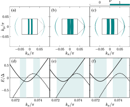
In this section, we study the phase transition between the phases III and IV in Fig. 2(a) of the main text. In what follows, we fix and , and vary the strength of the Rashba SOC . Other parameters are chosen to be the same as those in the main text. The phase boundary between the phases III and IV is located at . In Figs. S1(a), (b), and (c), we show the determinant index , Eq. (5), in the two-dimensional Brillouin zone for the parameters (phase IV), 0.083 (phase boundary), and 0.12 (phase III), respectively. We observe that with increasing , the two pairs of BFSs approach each other, until they merge at , and then separate again.
In Figs. S1(d), (e), and (f), we show the energy dispersion of the momentum space Hamiltonian , Eq. (S7), for the same parameters as in Figs. S1(a), (b), and (c), respectively, for fixed and as a function of . Here, we focus on the pair of BFSs at 3’o clock, i.e., near . We observe two parabolas, one with positive curvature and one with negative curvature, whose crossing points with the Fermi level define the BFSs. This is indicated by the shaded regions, which correspond to the momenta inside the BFSs. Interestingly, in phase IV the positive-curvature and negative-curvature parabolas intersect each other [panel (a)], while in phase III they avoid each other [panel (f)]. At the phase transition the two parabolas touch each other [panel (a)], such that the two pairs of BFSs merge together. Hence, the transition from phase III to phase IV represent a Lifshitz-type transition, where the topology of the BFSs changes.
S3 Additional figures of the differential conductance
In Fig. S2(a) we show the normalized differential conductance as a function of bias voltage in the absence of a Zeeman field, i.e., for . In this case the spectra of the BdG Hamiltonian are symmetric with respect to zero energy for any fixed , due to time-reversal and particle-hole symmetry. This leads to completely symmetric differential conductance spectra, i.e., does not change upon reversing the bias voltage. In the device of Fig. 1 the parent superconductor with pairing gap induces a smaller gap in the semiconductor, i.e., . This leads to three different voltage regimes with different conductance characteristics. Let us first discuss this for the case of perfect junction transparency (dashed line): (i) For bias voltage larger than there is no Andreev reflection possible leading to , (ii) for bias voltage smaller than but larger than , Andreev reflection occurs only for electrons with suitable momenta, mostly via the parent superconductor, leading to , and (iii) for bias voltage smaller then , perfect Andreev reflection is possible for all incident electrons, yielding . Accordingly, we observe in the tunneling limit (solid line) sharp peaks at the boundary of these regimes.
In Fig. S2(b) we show the normalized differential conductance for opposite field orientations, i.e., for and with (see solid and dashed lines, respectively). In the presence of a Zeeman field with the BdG spectra acquire an energy shift which scales linearly with and with an opposite sign for the two BdG bands Yuan and Fu (2018). Thus, the BdG spectra are no longer symmetric with respect to zero-energy for fixed , in line with the broken time-reversal symmetry. As a consequence, the three voltage regimes discussed above shift in an asymmetric fashion with respect to zero energy, as can be seen in Fig. S2(b) and Figs. 3(f)-(h). Note that upon flipping the sign of the Zeeman potential (i.e., by letting ) the energy shifts of the BdG spectra change sign, leading to a reflection of the differential conductance spectra with respect to zero-energy (compare solid and dashed lines).