On-chip low-loss all-optical MoSe2 modulator
Abstract
Monolayer transition metal dichalcogenides (TMDCs), like MoS2, MoSe2, WS2, and WSe2, feature direct bandgaps, strong spin-orbit coupling, and exciton-polariton interactions at the atomic scale, which could be harnessed for efficient light emission, valleytronics, and polaritonic lasing, respectively. Nevertheless, to build next-generation photonic devices that make use of these features, it is first essential to model the all-optical control mechanisms in TMDCs. Herein, a simple model is proposed to quantify the performance of a 35 µm long Si3N4 waveguide-integrated all-optical MoSe2 modulator. Using this model, a switching energy of 14.6 pJ is obtained for a transverse-magnetic (TM) and transverse-electric (TE) polarised pump signals at 480 nm. Moreover, maximal extinction ratios of 20.6 dB and 20.1 dB are achieved for a TM and TE polarised probe signal at 500 nm, respectively, with an ultra-low insertion loss of dB. Moreover, the device operates with an ultrafast recovery time of 50 ps, while maintaining a high extinction ratio for practical applications. These findings facilitate modeling and designing novel TMDC-based photonic devices.
Two-dimensional (2D) materials have recently emerged as practical active materials for on-chip photonics [1, 2, 3]. Unlike bulk materials, these materials are easily integrated into underlying substrates by van der Waals (vdW) forces, which facilitate device fabrication by complementary metal-oxide semiconductor (CMOS) processes [4]. Moreover, these materials exhibit unique optoelectronic properties that are of interest from a scientific and technological perspective. In particular, monolayer transition metal dichalcogenides (TMDCs) have direct bandgaps, strong spin-orbit coupling, and exciton-polariton interactions at the atomic scale, which could be utilized for efficient light emission, valleytronics, and polaritonic lasing, respectively [5, 6, 7, 8]. To design and build functional devices that make use of these features, it is first essential to model the electrical and all-optical control mechanisms in TMDCs. So far, there has not been a comprehensive model that describes these mechanisms in TMDC monolayers. To fill this gap, we model the saturable absorption and all-optical modulation mechanisms in monolayer molybdenum diselenide (MoSe2), which is integrated into silicon nitride (Si3N4) waveguides. To the best of our knowledge, a waveguide-integrated all-optical MoSe2 modulator has not been reported in the literature. This model can also describe these mechanisms in other TMDCs and 2D semiconductors.
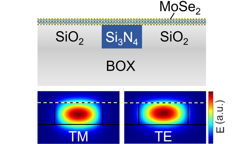
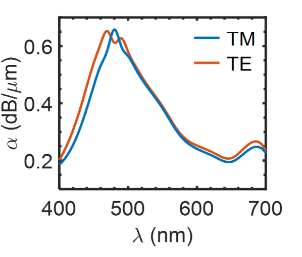
The device structure is presented in Fig. 1. A nm Si3N4 wire waveguide on top of a µm thick buried oxide (BOX) layer guides the incoming light to the modulator section, where the MoSe2 monolayer is located. The waveguide dimensions are optimized to achieve an ultra-low propagation loss. Si3N4 waveguides with similar dimensions have been demonstrated in [9], where the optical mode is guided with a propagation loss of merely 1.7 dB/cm. The waveguide supports the transverse-magnetic (TM) and transverse-electric (TE) modes. The computed absorption coefficient () of each mode is presented in Fig. 2a, which is attributed to the MoSe2 monolayer because it is the only absorbing material within the structure. Highly efficient coupling (%) between the Si3N4 waveguide and the modulator section is obtained for both modes, as shown in Fig. 2b. Simulations were conducted in Lumerical MODE with a 0.7 nm thick MoSe2 monolayer. The refractive index data of monolayer MoSe2 are taken from [10]. Perfect matching layer (PML) boundary conditions were used in the simulations. Similar results are obtained using metal boundary conditions.
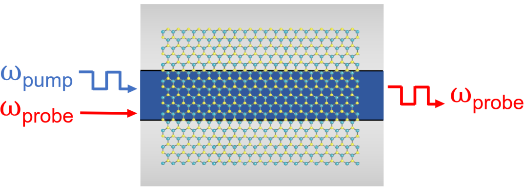
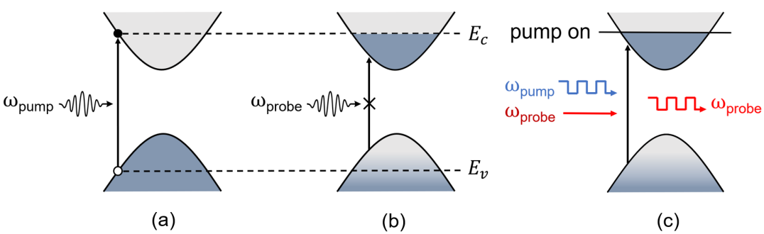
The modulation relies on the exciton bleaching mechanism [11]. As depicted in Fig. 3a, the MoSe2 monolayer absorbs an incident pump signal photon, which generates an interband exciton at visible wavelengths. When a sufficiently intense pump signal is applied, exciton bleaching occurs because of electron-hole plasma screening or band filling [12]. Due to the reduced dimensionality in 2D materials, screening is reduced. Then, exciton bleaching is most likely due to band filling [11]. Taking that into account, when the generated excitons fill the conduction and valence band states, a probe signal photon with an energy is transmitted, as shown in Fig. 3b. By taking advantage of this phenomenon, amplitude modulation is realized [13], where the probe signal is HIGH when the pump signal is ON, whereas it is LOW when the pump signal is OFF, as shown in Fig. 3c. Herein, the band structure of monolayer MoSe2 is described by the dispersion relations of the conduction () and valence () bands:
| (1) |
| (2) |
where eV is the energy bandgap [14], and are the effective masses of electrons and holes in monolayer MoSe2 [15], respectively, and is the wavevector, with being the carrier density. For a pump signal photon with an energy , transitions are blocked when the photogenerated excitons fully occupy the states. From Fig. 3, this occurs when:
| (3) |
where is the reduced effective mass. The corresponding photogenerated exciton density is given by:
| (4) |
Then, the switching energy of the modulator () is calculated by multiplying the total number of photogenerated excitons () by [16]:
| (5) |
where is the total number of photogenerated excitons, is the waveguide width, and is the modulator length. For µm, % of the pump signal is absorbed for both the TM and TE polarisations, where the absorbed power fraction () is calculated using the Beer-Lambert Law . A fraction of the absorbed light power is non-saturable (), and does not contribute to the modulation mechanism. Besides, there is a small coupling loss, , between the Si3N4 waveguide and the modulator section. To account for these losses, the effective switching energy () is calculated as [13]:
| (6) |
where is taken based on the values reported for a MoSe2 monolayer in [17]. is the Si3N4 waveguide loss that is not related to MoSe2, where dB/cm. In Fig. 2a), the absorption peak of the waveguide-integrated MoSe2 occurs at nm, which is chosen as the pump signal wavelength. The resulting is pJ for both the TE- and TM-polarised modes, where the absorption coefficients of both modes at that wavelength are almost similar.
The modulation efficiency is quantified by the extinction ratio (), where [13]. and represent the transmittance of the probe signal when the pump signal is switched ON and OFF, respectively. Here, we consider operation where a pump signal with an energy is applied. Then, and are given by [18]:
| (7) |
| (8) |
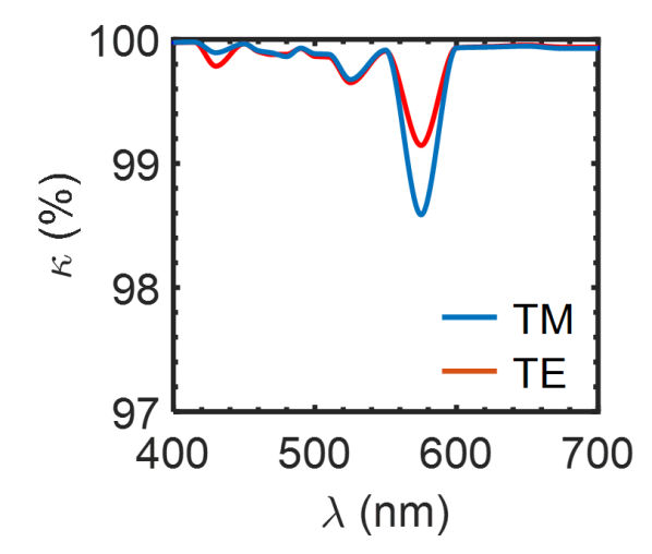
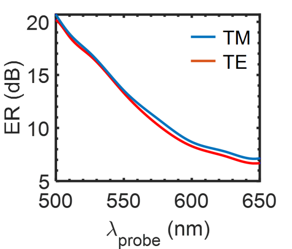
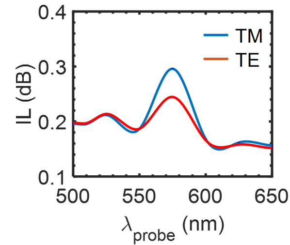
where is the absorbance calculated using the Beer-Lambert law. In addition, the insertion loss () of the device is calculated as . The resulting and of the device are presented in Fig. 4 for a broadband wavelength region. First, it is found that the is as low as dB across the studied band, which is attributed to the ultra-low coupling loss of the modulator. A remarkable ratio of 20.6 dB and 20.1 dB are achievable for a 500 nm probe signal with the TM and TE polarisations, respectively. Moreover, the plot follows the trend of the absorption coefficient plot that was presented in Fig. 2a. A higher absorption of the probe signal results in a greater extinction ratio between and . Additionally, highly efficient modulation is attainable at other wavelengths, where the lowest is 7.1 dB and 6.7 dB for the TM and TE polarised modes, respectively, at nm.
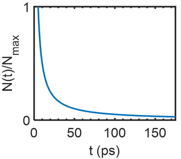
The modulation performance of the device is characterized by its recovery time, which is fundamentally limited by the cooling mechanisms in the MoSe2 monolayer. Following photoexcitation by a pump signal, exciton-exciton annihilation occurs within a few tens of picoseconds, while full electron-hole recombination can last for hundreds of picoseconds [19]. The cooling dynamics in monolayer MoSe2 can be modelled as [19]:
| (9) |
where is the exciton density as a function of time, is the initial exciton density, and cm2/s is the exciton-exciton annihilation rate [19]. At nm, the photogenerated exciton density is cm-2. Using these parameters, Eq. 9 is plotted in the time range of ps in Fig, 5, which is similar to the one presented in [19]. It is observed that recovery mostly occurs within tens of picoseconds by the exciton-exciton annihilation process. As previously explained, photogenerated excitons fill the states, leading to exciton bleaching and transmission of the probe signal. Therefore, the transmission of the probe signal follows the trend of the plotted curve in Fig. 5. Even though full recombination occurs in hundreds of picoseconds, for practical switching applications, it would be sufficient to operate the modulator with a time interval of 50 ps following a pump excitation, where the corresponding %. In compensation for faster operation, the decreases because of the reduced contrast between the ON and OFF states. For instance, for a negligible coupling and non-saturable losses, dB, where %, and %. However, while operating at a 50 ps time interval, %, and %, resulting in a 10 dB extinction ratio, which is highly desirable for practical applications. The ultrafast response of this device could be harnessed for building saturable absorbers, pulsed lasers, and for visible light switches. Moreover, the proposed model can describe the saturable absorption and all-optical modulation mechanisms in other TMDCs and 2D semiconductors by tuning the modelling parameters, e.g., material absorption, bandgap, effective masses, and exciton-exciton annihilation rate.
Funding Australian Research Council (DP200101353).
Acknowledgments This work was supported by the Australian Research Council (DP200101353).
Disclosures The authors declare no conflicts of interest.
Data Availability Statement The authors confirm that the data supporting the findings of this study are available within the article.
References
- [1] Z. Sun, A. Martinez, and F. Wang, \JournalTitleNature Photonics 10, 227 (2016).
- [2] D. Akinwande, C. Huyghebaert, C.-H. Wang, M. I. Serna, S. Goossens, L.-J. Li, H.-S. P. Wong, and F. H. Koppens, \JournalTitleNature 573, 507 (2019).
- [3] M. Alaloul and J. B. Khurgin, \JournalTitleIEEE Photonics Journal 13, 1 (2021).
- [4] M. Alaloul and M. Rasras, \JournalTitleJOSA B 38, 602 (2021).
- [5] L. Huang, A. Krasnok, A. Alu, Y. Yu, D. Neshev, and A. Miroshnichenko, \JournalTitleReports on Progress in Physics 85, 046401 (2021).
- [6] A. Rauschenbeutel and P. Schneeweiss, \JournalTitleNature Photonics 16, 261 (2022).
- [7] A. Kavokin, T. C. Liew, C. Schneider, P. G. Lagoudakis, S. Klembt, and S. Hoefling, \JournalTitleNature Reviews Physics pp. 1–17 (2022).
- [8] H. Ou, H. Matsuoka, J. Tempia, T. Yamada, T. Takahashi, K. Oi, Y. Takaguchi, T. Endo, Y. Miyata, C.-H. Chen et al., \JournalTitleACS nano 15, 12911 (2021).
- [9] A. Buchberger, J. Pulko, D. Morecroft, O. Basso, J. Kraft, and A. Bergmann, “Modelling propagation loss of pecvd silicon nitride strip waveguides: Evaluation and assessment of width dependency,” in 2021 Conference on Lasers and Electro-Optics (CLEO), (IEEE, 2021), pp. 1–2.
- [10] C. Hsu, R. Frisenda, R. Schmidt, A. Arora, S. M. De Vasconcellos, R. Bratschitsch, H. S. van der Zant, and A. Castellanos-Gomez, \JournalTitleAdvanced optical materials 7, 1900239 (2019).
- [11] R. Amin, J. B. Khurgin, and V. J. Sorger, \JournalTitleOptics express 26, 15445 (2018).
- [12] D. S. Chemla and D. A. Miller, \JournalTitleJOSA B 2, 1155 (1985).
- [13] M. Alaloul and J. B. Khurgin, \JournalTitleIEEE Journal of Selected Topics in Quantum Electronics 28, 1 (2022).
- [14] S. Tongay, J. Zhou, C. Ataca, K. Lo, T. S. Matthews, J. Li, J. C. Grossman, and J. Wu, \JournalTitleNano letters 12, 5576 (2012).
- [15] A. Rawat, N. Jena, A. De Sarkar et al., \JournalTitleJournal of Materials Chemistry A 6, 8693 (2018).
- [16] M. Alaloul and M. Rasras, \JournalTitleACS omega 6, 7576 (2021).
- [17] X. Tian, R. Wei, Z. Ma, and J. Qiu, \JournalTitleACS Applied Materials & Interfaces 14, 8274 (2022).
- [18] M. Alaloul and J. B. Khurgin, \JournalTitleOptics Express 30, 1950 (2022).
- [19] B. Liu, Y. Meng, X. Ruan, F. Wang, W. Liu, F. Song, X. Wang, J. Wu, L. He, R. Zhang et al., \JournalTitleNanoscale 9, 18546 (2017).
sample