Cavity-Enhanced 2D Material Quantum Emitters Deterministically Integrated with Silicon Nitride Microresonators
Abstract
Optically active defects in 2D materials, such as hexagonal boron nitride (hBN) and transition metal dichalcogenides (TMDs), are an attractive class of single-photon emitters with high brightness, room-temperature operation, site-specific engineering of emitter arrays, and tunability with external strain and electric fields. In this work, we demonstrate a novel approach to precisely align and embed hBN and TMDs within background-free silicon nitride microring resonators. Through the Purcell effect, high-purity hBN emitters exhibit a cavity-enhanced spectral coupling efficiency up to at room temperature, which exceeds the theoretical limit for cavity-free waveguide-emitter coupling and previous demonstrations by nearly an order-of-magnitude. The devices are fabricated with a CMOS-compatible process and exhibit no degradation of the 2D material optical properties, robustness to thermal annealing, and 100 nm positioning accuracy of quantum emitters within single-mode waveguides, opening a path for scalable quantum photonic chips with on-demand single-photon sources.
Introduction
Solid-state single-quantum emitters (SQEs) integrated with chip-scale photonic circuitry are a key building block for quantum information technologies Lodahl, Mahmoodian, and Stobbe (2015); Senellart, Solomon, and White (2017); Moody et al. (2022). Numerous SQEs capable of high-purity emission at room-temperature have been discovered in several host materials, including diamondAharonovich et al. (2011), silicon nitrideSenichev et al. (2021), and hexagonal boron nitride (hBN)Tran et al. (2016a). The integration of SQEs with CMOS-compatible photonic platforms would address a long-standing need for combining the manufacturability and scalability inherent to silicon-based photonics with materials that host high-quality SQEs. Heterogeneous integration techniques have led to successful demonstrations at cryogenic temperatures, including arrays of SQEs in diamond coupled to aluminum nitride photonic integrated circuits (PICs)Wan et al. (2020) and self-assembled quantum dots integrated with silicon nitrideDavanco et al. (2017); Chanana et al. (2022). Yet, scalable strategies for the integration of SQEs operating at room temperature with silicon-based PICs have not yet been demonstrated. Four key requirements are necessary to address this challenge: (1) A host material with high-purity and bright emitters at room temperature; (2) the ability to reliably integrate the SQE host material with the PIC platform without altering the optical properties; (3) control of the emission wavelength and precise alignment within low-loss and background-free single-mode waveguide structures; and (4) integration with microresonators for efficient emission into a single optical mode through the Purcell effect.
Of the SQE platforms, defect-type emitters in 2D materials Toth and Aharonovich (2019); Kianinia et al. (2022); Turunen et al. (2022); Azzam, Parto, and Moody (2021) have emerged as an attractive approach for engineering high-quality single-photon sources. SQEs have been identified in several monolayer and few-layer 2D materials spanning ultra-violet to telecommunications wavelengths, including hBNTran et al. (2016a, b); Fournier et al. (2020), transition metal dichalcogenides (TMDs) Koperski et al. (2015); Srivastava et al. (2015); Tonndorf et al. (2015); He et al. (2015); Chakraborty et al. (2015); Branny et al. (2016); Chakraborty, Goodfellow, and Vamivakas (2016); Zhao et al. (2021), and heterostructures Baek et al. (2020); Zhao et al. (2021). In hBN and WSe2, above MHz emission rates Grosso et al. (2017); Luo et al. (2018) and 95 single-photon purity have been reported. Through strain and defect engineering, emitters can be aligned into arrays Palacios-Berraquero et al. (2017); Parto et al. (2021), and nanophotonic integration further enhances their brightness Luo et al. (2019); Sortino et al. (2021). SQEs in hBN are particularly appealing due to a 5.7 eV bandgap, which enables room temperature generation of single photons with up to 93 purity Grosso et al. (2017).
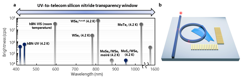
Thin layers of 2D materials can be aligned and placed onto a variety of substrates with automated dry-transfer techniques. These methods have enabled the integration of WSe2 and hBN with silicon nitridePeyskens et al. (2019); Errando-Herranz et al. (2021); Elshaari et al. (2021), which is an excellent photonic platform due to its mature fabrication, low propagation lossPuckett et al. (2021), large refractive indexSoref (2010), and wide transparency window that spans all of the identified 2D material SQEs, as shown in Fig. 1a; however, commonly used stoichiometric silicon nitride (Si3N4) has a strong background emission that overlaps with many SQEsElshaari et al. (2021), degrading single-photon purity. Previous on-chip integration strategies have placed hBN and WSe2 directly above or below waveguides, which has limited the coupling efficiency to only a few percent. Low coupling is exacerbated by the random position and dipole orientation of the SQEsPeyskens et al. (2019); Errando-Herranz et al. (2021); Kim et al. (2019); Li et al. (2021). Even for perfectly positioned and aligned emitters embedded in a single-mode waveguide, the theoretical maximum coupling efficiency is limited to .
Here, we demonstrate a novel method for efficient on-chip coupling by integrating 2D SQEs with a waveguide-coupled microring resonators using a CMOS-compatible process. Our approach is universal in that it enables the deterministic integration of SQEs with low auto-fluorescing, single-mode silicon nitride photonic circuits with precise control over the emitter placement and dipole orientation within the waveguiding structures—both of which are critical for achieving efficient emitter-mode coupling. As an example, we demonstrate an important advancement for quantum PICs by aligning an hBN SQE generating high-purity single photons at room temperature with a waveguide-coupled microring resonator (Fig. 1b). We demonstrate emitter-cavity coupling, which requires only a modest Purcell factor of to surpass the waveguide coupling efficiency in prior studies by nearly an order-of-magnitudeKim et al. (2019); Elshaari et al. (2021); Li et al. (2021). We demonstrate the universality of the approach by coupling exciton emission from embedded WS2 achieving > efficiency with a Purcell factor of . We present various emitter-microresonator designs, coupling schemes, and metrics that provide a roadmap for the integration of SQEs spanning the UV to telecommunications wavelength regimes. Guided by a semi-classical cavity-emitter model, routes towards achieving high-purity and high-indistinguishability single-photon emission from a variety of 2D material emitters are proposed, paving the way for enabling scalable and manufacturable integrated quantum photonics with on-demand sources in silicon nitride.
2D-compatible, low-emission silicon nitride
Standard plasma-enhanced chemical vapor deposition (PECVD) of stoichiometric Si3N4 suffers from significant background fluorescence at visible wavelengthsElshaari et al. (2021); Smith et al. (2020); Senichev et al. (2021), which is a problem for many 2D materials that emit in this range including hBN and TMDs. To address these challenges, we extend on previous developments of nitrogen-rich silicon nitride (SiN) that eliminate the background fluorescence. Careful tuning of the PECVD RF power, voltage bias, and silane to ammonia ratio (R) allows for the deposition of high-quality silicon nitride with negligible background fluorescence and high refractive index, without damaging the underlying 2D materials (Figure 2).
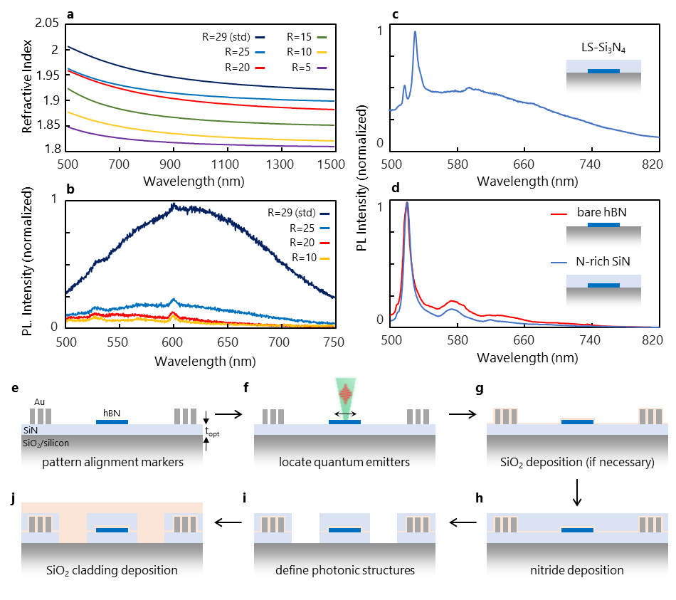
Similar to previous studiesAustin et al. (1985); Kistner et al. (2011); Senichev et al. (2021), we find that for decreasing , the background fluorescence quenches with only a moderate reduction in the refractive index; however, creating SQEs in hBN is typically achieved Vogl et al. (2018) through rapid thermal annealing up to 1100 °C. In previous studies, annealing has introduced or activated defects, which enhances the broad fluorescence background even in nitrogen-rich films (see supplementary material); however, by pre-conditioning the annealing chamber with an optimized oxygen/nitrogen environment, the formation of the defect band in SiN thin films annealed up to 1000 °C remains negligible. This points to extrinsic defects being introduced from the PECVD chamber into the nitride films as one of the primary sources of broadband fluorescence, which warrants future follow-up investigations. Up to now, the inability to anneal nitride thin films has been a severe limitation for site-controlled integration of 2D materialsElshaari et al. (2021), particularly hBN, aligned and integrated with waveguides for optimal mode coupling.
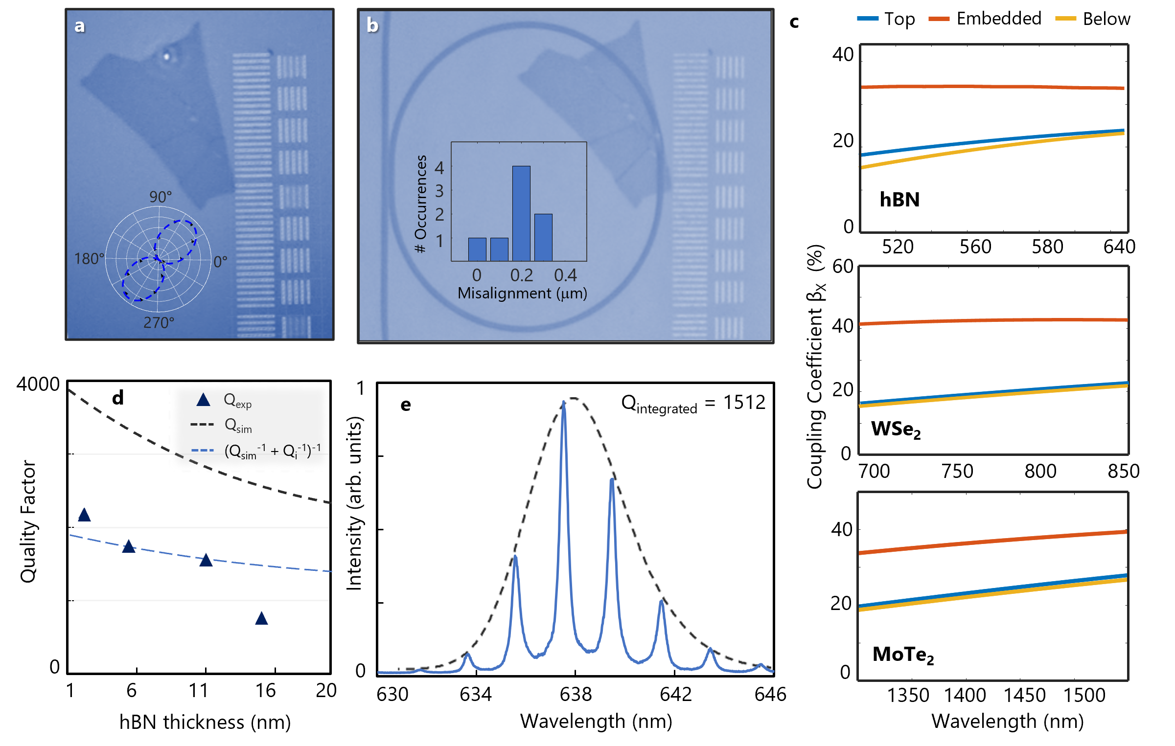
Figure 2c illustrates the results from this process. A room temperature photoluminescence spectrum is shown in Fig. 2c from a representative hBN emitter in a flake under a 100-nm-thick low-stress stoichiometric Si3N4 film (see supplementary information). Nearly 50 of the emission at the zero-phonon line (ZPL) wavelength of the emitter near 540 nm arises from the broad background emission from Si3N4. Using the new thin-film deposition procedure, we observe pristine emission from hBN emitters with negligible background from the SiN, shown in Fig. 2d for bare hBN (red curve) and the same hBN post growth and anneal of 100 nm of SiN (blue curve).
Microresonator Design and Integration
The fabrication process for deterministically embedding 2D flakes within SiN photonic structures is illustrated in Fig. 2(e-h) and described in more detail in the methods section and the supplementary information. A custom microscope integrated with a micro-photoluminescence (micro-PL) setup enables pre-screened SQEs to be aligned to microresonators with 100-nm precision. To do this, first gold alignment marks are patterned near the SQE flake using electron-beam lithography and lift-off techniques. The flake is screened for SQEs using polarization-resolved micro-PL to determine their position and dipole orientation with 100-nm and precision, respectively, using edge detection and image matrix transformation techniques. The combination of precise SQE placement and orientation with low-background, damage-free SiN deposition are the key enabling capabilities for 2D material PIC integration with single-mode photonic structures, which has proven to be difficult for randomly positioned SQEs. Since the PECVD process and annealing can be used to directly grow the SiN layer on top of the hBN SQE without altering its spectrum and single-photon purity, the flake can be integrated either on the top, in the middle, or underneath the structures.
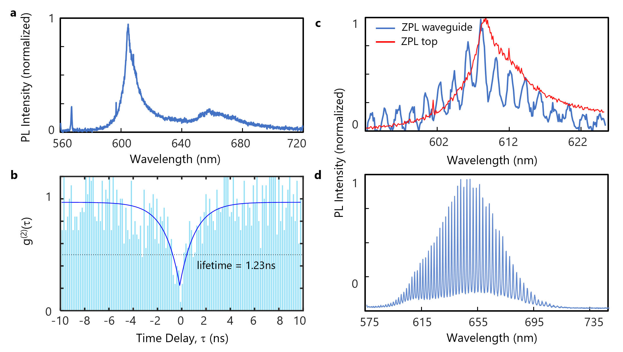
Figure 3c demonstrates the theoretical coupling efficiency of a dipole emitter with perfect polarization alignment integrated with a single-mode SiN waveguide at different heights for three common types of SQEs in 2D materials. The coupling efficiency of the radiated field into the optical mode, normalized to the total radiated field, is defined as , where corresponds to emission into the waveguide mode. Intuitively, the greatest mode overlap occurs when flakes are embedded in the center of the waveguide; however, care must be taken to avoid etched hBN edges within a few hundred nanometers to the emitter, which we have found can introduce edge states that alter the charge state of the defect or act as charge traps that contribute to optical dephasing and spectral diffusion. To avoid these complications, we also explored the integration of hBN underneath the waveguiding structures in which the hBN flake is not exposed to any etched surfaces. For this configuration, a theoretical coupling efficiency of (Fig. 2c) is anticipated for waveguide-integrated SQEs. In practice, the measured waveguide coupling efficiency, however, is typically limited to primarily due to poor SQE-mode overlap and dipole misalignmentLi et al. (2021); Kim et al. (2019).
Alternatively, can be enhanced relative to waveguides by integrating the emitter within a microring resonator. For a cavity-coupled emitter, its radiative decay rate is resonantly enhanced and becomes , where is the radiative decay rate in the absence of the cavity and is the radiative enhancement due to the cavity Gould et al. (2016); Faraon et al. (2011). This enhancement can be quantified through the Purcell factor where , , and are the refractive index, quality factor, and mode-volume of the cavity. It is important to point out that for an emitter weakly coupled to the cavity, it is often assumed that the density of states of the free-space modes remains undisturbedFaraon et al. (2011); Fox, Fox et al. (2006). As a result, for a cavity-coupled emitter can be expressed as . This has important implications for exploiting resonant cavity effects: increasing , and thus , amounts to designing high cavities with small mode volume. As we show below, even for , the SQE emission into a photonic circuit can be significantly enhanced relative to an emitter coupled to a waveguide, motivating the need for on-chip cavity enhancement.
The Purcell factor is typically defined in the "good-emitter" regime in which the cavity linewidth is larger than the SQE linewidth ; however, in many instances, including hBN emitters at room temperature, phonon-induced dephasing broadens the ZPL width beyond the radiative limit, and the cavity-coupled system is found in the so-called “bad-emitter” regime, i.e. , where only a portion of the SQE ZPL couples into the cavity. This effectively reduces the traditional Purcell factor to , where heuristically represents the ratio of the radiated power from the SQE that overlaps with the cavity mode. In the bad emitter regime, a wavelength dependent Purcell factor and coupling efficiency can be defined as a function of the spectral power of the emitter and are given by and where and are the spectral intensity of the emitter into the cavity mode and into free-space, respectively. This, in effect, negates the factor and allows for the enhancement of the portion of the ZPL that is resonantly coupled to the cavity to be quantified regardless of the emitter-cavity regimeKaupp et al. (2013). Whether in the good- or bad-emitter regime, specifies the cavity enhancement at the emission wavelength , while integration over determines the total . For waveguide-coupled emitters without any resonant effects, .
As shown below, to maximize the total system efficiency, should be chosen to be in an intermediate region between the good- and bad-emitter regimes. Hence, we chose a racetrack resonator configuration with a 100-nm-thick and 600-nm-wide cross section, a 3-m-long coupler region that results in a free spectral range (FSR) of 2 nm, a mode-volume of at the resonance of interest around 610 nm, and a simulated quality factor of 7000, which is comparable to the cryogenic linewidth of hBN emitters observed in our samples. We first characterized resonators without embedded 2D materials to establish a baseline for our quality factor, which we can write as , where corresponds to the bare resonator, corresponds to the coupling to the waveguide, and arises from additional scattering from an integrated 2D flake. Measurements from 10 nominally identical resonators from three different fabrication runs yield an average and , which results in a slightly lower than our simulations likely due to etched sidewall roughness and a larger waveguide-resonator coupling gap.
We next examined the impact of integrated hBN flakes on the resonator . As expected, with increasing flake thickness, decreases, which matches our simulations (Fig. 3d). While hBN has a similar refractive index as SiN, light scattering at the SiN-hBN interfaces, which has a more pronounced effect for thicker flakes, dominates the loss and reduction of in our simulations. Experimentally, for flakes with a thickness exceeding 30 nm, decreases by an order-of-magnitude. Given that hBN emitters tend to have narrower linewidth and brighter emission in thin, but multilayer flakes, this result confirms an important design trade-off for resonator integration. We found that emitters with linewidths as narrow as 3-4 nm at room temperature are routinely identified in -nm-thick flakes. Figure 3e shows the spectrum of the microresonator with an hBN flake integrated below the ring, exhibiting a loaded . We note that while we focus on these emitters in this study as a demonstration, the integration strategy and fabrication procedure are entirely 2D materials agnostic. For example, as we later show, integration of 2D TMDs, unlike hBN, does not introduce significant scattering loss in the cavity and the remains close to the empty microring resonator.
Cavity-Enhanced 2D Material On-Chip Coupling
Figure 4a shows the photoluminescence (PL) spectrum of a representative hBN emitter after the complete device fabrication using top-down excitation and collection at room temperature. As demonstrated in Fig. 2d and Fig. 4a, the integration and fabrication do not degrade the quality of the emitter and we retain the background-free emission. The photon anti-bunching behavior verifying single-photon emission is illustrated in Fig. 4b in which (0.18 with background correction). We next excite the emitter using a 0.9 NA objective from above the resonator, and emission into the waveguide is collected into a single-mode fiber and sent to a spectrometer and charge-coupled-device camera. Figure 4c shows the integrated hBN SQE with the ZPL emission centered near 610 nm. The dashed line is emission collected from above the emitter, whereas the solid line is emission collected from the waveguide. Bright emission into the microresonator modes is clearly observed by the peaks imprinted on the ZPL emission spectrum separated by an FSR of 2 nm. A similar response is imprinted on the room temperature exciton emission from monolayer WS2 in Fig. 4d, demonstrating the universality of the approach for 2D material integration.
To extract the spectral Purcell enhancement and the spectral coupling efficiency , we follow a procedure previously reported for SQEs Kim et al. (2019); Li et al. (2021); Gould et al. (2016). Accounting for the optical loss in our system, the effective Purcell enhancement at the ZPL peak wavelength can be expressed as
| (1) |
where , , , , , , and are respectively the portion of the total free-space light collected by the top objective, efficiency of the top collection path, microring out-coupling efficiency, facet coupling efficiency, side path collection efficiency, spectral intensity measured on the CCD at the ZPL wavelength from the top objective, and spectral intensity measured from the waveguide output port (see supplementary information).
For the integrated emitter in Fig. 4c, a spectral Purcell factor up to corresponding to is measured on the ZPL resonance ( integrated across the entire spectrum). The deviation from the theoretical estimate of the effective Purcell factor for this system (equal to 1.7) can be attributed to small misalignment and dipole orientation inaccuracies. Importantly, even though is close to unity, this results in nearly half of the emission now coupled into the cavity mode. This is best reflected in of the cavity-coupled system. Here, even the lower-bound of our measured exceeds the maximum theoretical coupling efficiency into a waveguide of the same configuration ( as shown in Fig. 2). Similarly for the integrated WS2, is obtained, amounting to a spectral Purcell factor of . The higher measured Purcell factor for WS2 is due to the fact that it is thinner, and thus it does not significantly alter the loaded quality factor of the resonator.
Discussion
To design a 2D quantum emitter-cavity system, it is important to consider the total PIC efficiency, which can be expressed as , where is the quantum efficiency of the emitter and is the extraction efficiency of the coupled light in the cavity into the bus waveguideThomas et al. (2014); Gould et al. (2016). Maximizing is a multi-variable problem because the individual component efficiencies cannot be adjusted independently. For instance, one can reach the over-coupled regime using a small waveguide-resonator gap or a pulley coupled bus waveguide, which leads to as decreases; however, a significant reduction of lowers the enhancement and the factor. Similarly, while a high results in a larger , for large , the cavity-emitter system can enter the bad-emitter regime where only a portion of the ZPL will couple into the microring resonator and will begin to decrease. Generally, the linewidth of the emitter sets a practical upper bound for the loaded . While this can imply that SQEs with the narrowest linewidth are more suitable for cavity integration, it should be noted that the SQE internal quantum efficiency plays an important role in the emitter-cavity design. For instance, at cryogenic temperatures, while WSe2 SQEs have a relatively narrow linewidth (eV) compared to hBN emitters, for WSe2 has been estimatedLuo et al. (2019); Parto et al. (2021) to be only compared to up to reported for hBNNikolay et al. (2019). Therefore, to optimize the cavity design with high system-wide efficiency for different 2D emitters, a holistic approach must be considered.
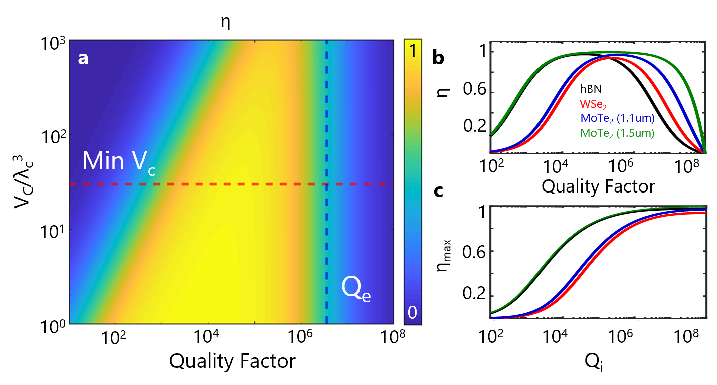
In Fig. 5, we explore the performance of a 2D SQE-cavity system using solutions to the Jaynes-Cummings Hamiltonian for a two-level system interacting with a cavity (see supplementary information). Initially, we set to to explore the regime in which the coupling governs and its effect on . Figure 5a shows as function of mode volume and the microresonator quality factor for hBN emitters at cryogenic temperatures, where it assumed that pure dephasing from phonons is negligible and the linewidth is governed by recombination. The vertical dashed line sets the boundary of the bad-emitter regime in which the total quality factor exceeds the emitter quality factor determined from its linewidth; as becomes larger than , only a portion of the emitter couples in to the cavity. The horizontal dashed line in Fig. 5a indicates the minimum mode volume for our PICs (), and slices along this line are shown in Fig. 5b for hBN and TMD emitters. For , up to is possible for hBN emitters at cryogenic temperatures. For exceeding , the system enters the bad-emitter regime and the extraction efficiency decreases.
Purcell enhancement can compensate for intrinsic low quantum efficiency of some emitter types, such as WSe2 and MoTe2 (m emission), provided loaded is reached for the platform. On the other hand, integration of emitters with high quantum efficiency, such as hBN and MoTe2 (1.5 m emission) can be realized at lower . At the moment, the primary limitation for achieving unity extraction efficiency for ideal 2D emitters is the intrinsic quality factor of the platform, which sets an upper bound on the achievable . This is shown in Fig. 5c, which represents the maximum attainable extraction efficiency for each class of the emitters as function of the intrinsic quality factor of the platform. As the intrinsic approaches , which is already achievable for different SiN waveguide aspect ratios, it is possible to integrate 2D quantum emitters with total efficiencies exceeding .
Taken together, our simulations and experiments provide a straightforward approach for deterministically aligning and orienting SQEs in 2D materials to on-chip microresonators with a route towards high coupling efficiency. Already this approach achieves coupling efficiency into the resonator at the emitter ZPL resonance, which is an order of magnitude higher than waveguide coupling for hBN. System-wide efficiency approaching can be attained in the near-term with modest improvements to the microresonator and its design for over-coupling. The platform and methods developed in this work can serve as a stepping stone towards future demonstrations of on-chip 2D quantum emitter integration with high extraction efficiency, brightness, and indistinguishably. In the near future, by exploring SiN microresonators embedded with other SQEs with narrow linewidths, such as WSe2 and MoTe2, new opportunities exist for on-demand and site-controlled SQEs with silicon-based photonics for chip-scale quantum information applications.
Acknowledgements.
This work was supported by NSF Award No. ECCS-2032272 and the NSF Quantum Foundry through Q-AMASE-i program Award No. DMR-1906325. Experiments were performed with support from DURIP Award No. FA9550-21-1-0257. S.I.A. acknowledges support from the California NanoSystems Institute through the Elings fellowship. K.W. and T.T. acknowledge support from JSPS KAKENHI (Grant Numbers 19H05790, 20H00354, and 21H05233). K.P. and S.A. contributed equally to this work.Data Availability Statement
The data that support the findings in this study are available from the corresponding author upon reasonable request.
References
References
- Lodahl, Mahmoodian, and Stobbe (2015) P. Lodahl, S. Mahmoodian, and S. Stobbe, “Interfacing single photons and single quantum dots with photonic nanostructures,” Rev. Mod. Phys. 87, 347–400 (2015).
- Senellart, Solomon, and White (2017) P. Senellart, G. Solomon, and A. White, “High-performance semiconductor quantum-dot single-photon sources,” Nature Nanotechnology 12, 1026–1039 (2017).
- Moody et al. (2022) G. Moody, V. J. Sorger, D. J. Blumenthal, P. W. Juodawlkis, W. Loh, C. Sorace-Agaskar, A. E. Jones, K. C. Balram, J. C. F. Matthews, A. Laing, M. Davanco, L. Chang, J. E. Bowers, N. Quack, C. Galland, I. Aharonovich, M. A. Wolff, C. Schuck, N. Sinclair, M. Lončar, T. Komljenovic, D. Weld, S. Mookherjea, S. Buckley, M. Radulaski, S. Reitzenstein, B. Pingault, B. Machielse, D. Mukhopadhyay, A. Akimov, A. Zheltikov, G. S. Agarwal, K. Srinivasan, J. Lu, H. X. Tang, W. Jiang, T. P. McKenna, A. H. Safavi-Naeini, S. Steinhauer, A. W. Elshaari, V. Zwiller, P. S. Davids, N. Martinez, M. Gehl, J. Chiaverini, K. K. Mehta, J. Romero, N. B. Lingaraju, A. M. Weiner, D. Peace, R. Cernansky, M. Lobino, E. Diamanti, L. T. Vidarte, and R. M. Camacho, “2022 roadmap on integrated quantum photonics,” Journal of Physics: Photonics 4, 012501 (2022).
- Aharonovich et al. (2011) I. Aharonovich, S. Castelletto, D. A. Simpson, C.-H. Su, A. D. Greentree, and S. Prawer, “Diamond-based single-photon emitters,” Reports on Progress in Physics 74, 076501 (2011).
- Senichev et al. (2021) A. Senichev, S. Peana, Z. O. Martin, D. Sychev, X. Xu, Z. Kudyshev, A. S. Lagutchev, A. Boltasseva, and V. M. Shalaev, “Room-temperature single-photon emitters in silicon nitride,” in 2021 Conference on Lasers and Electro-Optics (CLEO) (IEEE, 2021).
- Tran et al. (2016a) T. T. Tran, K. Bray, M. J. Ford, M. Toth, and I. Aharonovich, “Quantum emission from hexagonal boron nitride monolayers,” Nature Nanotechnology 11, 37–41 (2016a).
- Wan et al. (2020) N. H. Wan, T.-J. Lu, K. C. Chen, M. P. Walsh, M. E. Trusheim, L. De Santis, E. A. Bersin, I. B. Harris, S. L. Mouradian, I. R. Christen, E. S. Bielejec, and D. Englund, “Large-scale integration of artificial atoms in hybrid photonic circuits,” Nature 583, 226–231 (2020).
- Davanco et al. (2017) M. Davanco, J. Liu, L. Sapienza, C.-Z. Zhang, J. V. De Miranda Cardoso, V. Verma, R. Mirin, S. W. Nam, L. Liu, and K. Srinivasan, “Heterogeneous integration for on-chip quantum photonic circuits with single quantum dot devices,” Nature Communications 8, 889 (2017).
- Chanana et al. (2022) A. Chanana, H. Larocque, R. Moreira, J. Carolan, B. Guha, V. Anant, J. D. Song, D. Englund, D. J. Blumenthal, K. Srinivasan, and M. Davanco, “Triggered single-photon generation and resonance fluorescence in ultra-low loss integrated photonic circuits,” (2022).
- Fournier et al. (2020) C. Fournier, A. Plaud, S. Roux, A. Pierret, M. Rosticher, K. Watanabe, T. Taniguchi, S. Buil, X. Quélin, J. Barjon, J. Barjon, J.-P. Hermier, and A. Delteil, “Position-controlled quantum emitters with reproducible emission wavelength in hexagonal boron nitride,” arXiv preprint arXiv:2011.12224 (2020).
- Gale et al. (2022) A. Gale, C. Li, Y. Chen, K. Watanabe, T. Taniguchi, I. Aharonovich, and M. Toth, “Site-specific fabrication of blue quantum emitters in hexagonal boron nitride,” ACS Photonics 9, 2170–2177 (2022).
- Grosso et al. (2017) G. Grosso, H. Moon, B. Lienhard, S. Ali, D. K. Efetov, M. M. Furchi, P. Jarillo-Herrero, M. J. Ford, I. Aharonovich, and D. Englund, “Tunable and high-purity room temperature single-photon emission from atomic defects in hexagonal boron nitride,” Nature Communications 8, 705 (2017).
- Luo et al. (2018) Y. Luo, G. D. Shepard, J. V. Ardelean, D. A. Rhodes, B. Kim, K. Barmak, J. C. Hone, and S. Strauf, “Deterministic coupling of site-controlled quantum emitters in monolayer WSe2 to plasmonic nanocavities,” Nature Nanotechnology 13, 1137–1142 (2018).
- Peyskens et al. (2019) F. Peyskens, C. Chakraborty, M. Muneeb, D. Van Thourhout, and D. Englund, “Integration of single photon emitters in 2D layered materials with a silicon nitride photonic chip,” Nature Communications 10, 4435 (2019).
- Zhao et al. (2021) H. Zhao, M. T. Pettes, Y. Zheng, and H. Htoon, “Site-controlled telecom-wavelength single-photon emitters in atomically-thin MoTe2,” Nature Communications 12, 6753 (2021).
- Zhao et al. (2022) H. Zhao, L. Zhu, X. Li, V. Chandrasekaran, J. K. Baldwin, M. T. Pettes, A. Piryatinski, L. Yang, and H. Htoon, “Manipulating interlayer excitons for ultra-pure near-infrared quantum light generation,” arXiv preprint arXiv:2205.02472 (2022).
- Baek et al. (2020) H. Baek, M. Brotons-Gisbert, Z. X. Koong, A. Campbell, M. Rambach, K. Watanabe, T. Taniguchi, and B. D. Gerardot, “Highly energy-tunable quantum light from moiré-trapped excitons,” Science Advances 6, eaba8526 (2020).
- Toth and Aharonovich (2019) M. Toth and I. Aharonovich, “Single photon sources in atomically thin materials,” Annual Review of Physical Chemistry 70, 123–142 (2019).
- Kianinia et al. (2022) M. Kianinia, Z.-Q. Xu, M. Toth, and I. Aharonovich, “Quantum emitters in 2D materials: Emitter engineering, photophysics, and integration in photonic nanostructures,” Applied Physics Reviews 9, 011306 (2022).
- Turunen et al. (2022) M. Turunen, M. Brotons-Gisbert, Y. Dai, Y. Wang, E. Scerri, C. Bonato, K. D. Jöns, Z. Sun, and B. D. Gerardot, “Quantum photonics with layered 2D materials,” Nature Reviews Physics 4, 219–236 (2022).
- Azzam, Parto, and Moody (2021) S. I. Azzam, K. Parto, and G. Moody, “Prospects and challenges of quantum emitters in 2D materials,” Applied Physics Letters 118, 240502 (2021).
- Tran et al. (2016b) T. T. Tran, C. Elbadawi, D. Totonjian, C. J. Lobo, G. Grosso, H. Moon, D. R. Englund, M. J. Ford, I. Aharonovich, and M. Toth, “Robust multicolor single photon emission from point defects in hexagonal boron nitride,” ACS Nano 10, 7331–7338 (2016b).
- Koperski et al. (2015) M. Koperski, K. Nogajewski, A. Arora, V. Cherkez, P. Mallet, J.-Y. Veuillen, J. Marcus, P. Kossacki, and M. Potemski, “Single photon emitters in exfoliated WSe2 structures,” Nature Nanotechnology 10, 503–506 (2015).
- Srivastava et al. (2015) A. Srivastava, M. Sidler, A. V. Allain, D. S. Lembke, A. Kis, and A. Imamoğlu, “Optically active quantum dots in monolayer WSe2,” Nature Nanotechnology 10, 491–496 (2015).
- Tonndorf et al. (2015) P. Tonndorf, R. Schmidt, R. Schneider, J. Kern, M. Buscema, G. A. Steele, A. Castellanos-Gomez, H. S. van der Zant, S. M. de Vasconcellos, and R. Bratschitsch, “Single-photon emission from localized excitons in an atomically thin semiconductor,” Optica 2, 347–352 (2015).
- He et al. (2015) Y.-M. He, G. Clark, J. R. Schaibley, Y. He, M.-C. Chen, Y.-J. Wei, X. Ding, Q. Zhang, W. Yao, X. Xu, C.-Y. Lu, and J.-W. Pan, “Single quantum emitters in monolayer semiconductors,” Nature Nanotechnology 10, 497–502 (2015).
- Chakraborty et al. (2015) C. Chakraborty, L. Kinnischtzke, K. M. Goodfellow, R. Beams, and A. N. Vamivakas, “Voltage-controlled quantum light from an atomically thin semiconductor,” Nature Nanotechnology 10, 507–511 (2015).
- Branny et al. (2016) A. Branny, G. Wang, S. Kumar, C. Robert, B. Lassagne, X. Marie, B. D. Gerardot, and B. Urbaszek, “Discrete quantum dot like emitters in monolayer MoSe2: spatial mapping, magneto-optics, and charge tuning,” Applied Physics Letters 108, 142101 (2016).
- Chakraborty, Goodfellow, and Vamivakas (2016) C. Chakraborty, K. M. Goodfellow, and A. N. Vamivakas, “Localized emission from defects in MoSe2 layers,” Optical Materials Express 6, 2081–2087 (2016).
- Palacios-Berraquero et al. (2017) C. Palacios-Berraquero, D. M. Kara, A. R.-P. Montblanch, M. Barbone, P. Latawiec, D. Yoon, A. K. Ott, M. Loncar, A. C. Ferrari, and M. Atatüre, “Large-scale quantum-emitter arrays in atomically thin semiconductors,” Nature Communications 8, 15093 (2017).
- Parto et al. (2021) K. Parto, S. I. Azzam, K. Banerjee, and G. Moody, “Defect and strain engineering of monolayer WSe2 enables site-controlled single-photon emission up to 150 K,” Nature Communications 12, 3585 (2021).
- Luo et al. (2019) Y. Luo, N. Liu, X. Li, J. C. Hone, and S. Strauf, “Single photon emission in WSe2 up 160 K by quantum yield control,” 2D Materials 6, 035017 (2019).
- Sortino et al. (2021) L. Sortino, P. G. Zotev, C. L. Phillips, A. J. Brash, J. Cambiasso, E. Marensi, A. M. Fox, S. A. Maier, R. Sapienza, and A. I. Tartakovskii, “Bright single photon emitters with enhanced quantum efficiency in a two-dimensional semiconductor coupled with dielectric nano-antennas,” Nature Communications 12, 6063 (2021).
- Errando-Herranz et al. (2021) C. Errando-Herranz, E. Schöll, R. Picard, M. Laini, S. Gyger, A. W. Elshaari, A. Branny, U. Wennberg, S. Barbat, T. Renaud, M. Sartison, M. Brotons-Gisbert, C. Bonato, B. D. Gerardot, V. Zwiller, and K. D. Jöns, “Resonance fluorescence from waveguide-coupled, strain-localized, two-dimensional quantum emitters,” ACS photonics 8, 1069–1076 (2021).
- Elshaari et al. (2021) A. W. Elshaari, A. Skalli, S. Gyger, M. Nurizzo, L. Schweickert, I. Esmaeil Zadeh, M. Svedendahl, S. Steinhauer, and V. Zwiller, “Deterministic integration of hBN emitter in silicon nitride photonic waveguide,” Advanced Quantum Technologies 4, 2100032 (2021).
- Puckett et al. (2021) M. W. Puckett, K. Liu, N. Chauhan, Q. Zhao, N. Jin, H. Cheng, J. Wu, R. O. Behunin, P. T. Rakich, K. D. Nelson, and D. J. Blumenthal, “422 million intrinsic quality factor planar integrated all-waveguide resonator with sub-MHz linewidth,” Nature Communications 12, 934 (2021).
- Soref (2010) R. Soref, “Mid-infrared photonics in silicon and germanium,” Nature Photonics 4, 495–497 (2010).
- Kim et al. (2019) S. Kim, N. M. H. Duong, M. Nguyen, T.-J. Lu, M. Kianinia, N. Mendelson, A. Solntsev, C. Bradac, D. R. Englund, and I. Aharonovich, “Integrated on chip platform with quantum emitters in layered materials,” Advanced Optical Materials 7, 1901132 (2019).
- Li et al. (2021) C. Li, J. E. Froch, M. Nonahal, T. N. Tran, M. Toth, S. Kim, and I. Aharonovich, “Integration of hBN quantum emitters in monolithically fabricated waveguides,” ACS Photonics 8, 2966–2972 (2021).
- Smith et al. (2020) J. Smith, J. Monroy-Ruz, J. G. Rarity, and K. C. Balram, “Single photon emission and single spin coherence of a nitrogen vacancy center encapsulated in silicon nitride,” Applied Physics Letters 116, 134001 (2020).
- Austin et al. (1985) I. G. Austin, W. A. Jackson, T. M. Searle, P. K. Bhat, and R. A. Gibson, “Photoluminescence properties of a-SiNx: H alloys,” Philosophical Magazine B 52, 271–288 (1985).
- Kistner et al. (2011) J. Kistner, X. Chen, Y. Weng, H. P. Strunk, M. B. Schubert, and J. H. Werner, “Photoluminescence from silicon nitride—no quantum effect,” Journal of Applied Physics 110, 023520 (2011).
- Vogl et al. (2018) T. Vogl, G. Campbell, B. C. Buchler, Y. Lu, and P. K. Lam, “Fabrication and deterministic transfer of high-quality quantum emitters in hexagonal boron nitride,” ACS Photonics 5, 2305–2312 (2018).
- Gould et al. (2016) M. Gould, E. R. Schmidgall, S. Dadgostar, F. Hatami, and K.-M. C. Fu, “Efficient extraction of zero-phonon-line photons from single nitrogen-vacancy centers in an integrated gap-on-diamond platform,” Physical Review Applied 6, 011001 (2016).
- Faraon et al. (2011) A. Faraon, P. E. Barclay, C. Santori, K.-M. C. Fu, and R. G. Beausoleil, “Resonant enhancement of the zero-phonon emission from a colour centre in a diamond cavity,” Nature Photonics 5, 301–305 (2011).
- Fox, Fox et al. (2006) A. M. Fox, M. Fox, et al., Quantum optics: an introduction, Vol. 15 (Oxford University Press, 2006).
- Kaupp et al. (2013) H. Kaupp, C. Deutsch, H.-C. Chang, J. Reichel, T. W. Hänsch, and D. Hunger, “Scaling laws of the cavity enhancement for nitrogen-vacancy centers in diamond,” Physical Review A 88, 053812 (2013).
- Nikolay et al. (2019) N. Nikolay, N. Mendelson, E. Özelci, B. Sontheimer, F. Böhm, G. Kewes, M. Toth, I. Aharonovich, and O. Benson, “Direct measurement of quantum efficiency of single-photon emitters in hexagonal boron nitride,” Optica 6, 1084–1088 (2019).
- Thomas et al. (2014) N. Thomas, R. J. Barbour, Y. Song, M. L. Lee, and K.-M. C. Fu, “Waveguide-integrated single-crystalline gap resonators on diamond,” Optics express 22, 13555–13564 (2014).
Methods
2D SQE compatible silicon nitride PECVD growth and anneal
The background-free integrated photonic platform was realized by growing 100 nm nitrogen-rich SiN films on 3 m thick thermal oxide substrates. All films were grown using a vision 310 advanced vacuum PECVD system at 300 °C and 800 mTorr with iterative 30 W, 13.56 MHz and 110 W, 187 kHz plasma steps for 8 and 1.5 seconds, respectively. The silane, ammonia, and nitrogen precursor flow rates were chosen to be 360 sccm, 18 sccm, and 980 sccm, respectively, to achieve nitrogen-rich growth conditions that quenches the SiN background emission while maintaining a high refractive index. A 20-minute, 1000 °C rapid thermal anneal was performed to create optically active defects in hBN that was first transferred onto the Si3N4. Annealing was carried out in a 100 sccm nitrogen and 100 sccm oxygen environment to create bright room temperature stable emitters in hBN without activating the SiN defect band.
Figure 2a shows the measured refractive index of SiN for (stoichiometric) to . With decreasing , the refractive index decreases from 2.01 to 1.86 at 500 nm. We find that at , the background fluorescence begins to quench, as shown in Fig. 2b. Because of the trade-off between the reduction of the refractive index and the fluorescence quenching with decreasing , we find that a ratio of provides sufficient background-free SiN with only a moderate reduction of the index. By fine-tuning the PECVD parameters, it is possible to simultaneously achieve quenching while maintaining a refractive index > 1.9 without degrading the optical quality of the embedded 2D materials.
Numerical Simulations
All simulations have been performed using Ansys Lumerical. Emitter-waveguide coupling efficiency has been calculated using Lumerical FDTD using a dipole source as an emitter. Coupling factor to the fundamental mode is calculated using a mode expansion monitor. Ring quality factor and free spectral range are simulated using Lumerical varFDTD with the fundamental TE mode source as an excitation. The mode volume of the cavity mode is calculated with FDTD using the formula . Top collection efficiency of the photoluminescence using high NA objective (0.95) are performed using Lumerical FDTD through the integration over the acceptance cone. More details on the simulations can be found in the supplementary information.
Photonic Device Fabrication
The fabrication process for integrating 2D quantum emitters within SiN photonic structures is illustrated in Fig. 2e-2j and is described in more detail in the supplementary information. Briefly, SiN thin films were grown by PECVD on a 3-m-thick SiO2 film on silicon, where the film thickness is determined by the desired position of the flake in the waveguide structure normal to the sample plane. A variety of SiN films were grown with an increasing ammonia-to-silane ratio to characterize the 2D material transfer, annealing, and full fabrication process. Using an all-dry visco-elastic transfer technique, 2D material flakes of hBN or WS2 are transferred within the electron-beam processing window of 200 200 m. For hBN flakes, a 5-minute, 250 watt O2 plasma and rapid thermal annealing step at 1000 °C activates the quantum emitters, which are then pre-screened by scanning the sample in a 0.9 numerical-aperture (NA) photoluminescence microscopy setup. The emission brightness and single-photon purity are the primary metrics we use to identify suitable emitters for integration. Once the target emitters and flakes are identified, electron-beam lithography and lift-off techniques are used to pattern metal alignment markers and a grid for subsequent electron-beam lithography steps. The grid allows for identification of emitters with 100-nm precision, which allows for post-fabrication of structures carefully aligned to the emitters. For transition metal dichalcogenides, we next deposit a thin ( 10 nm) film of PECVD SiO2 as a protection layer, which our simulations show has negligible impact on the confined optical modes, propagation loss, and resonator quality factor. Next, the remaining SiN thin film is grown, followed by an electron-beam lithography and reactive-ion etching step, and finally an optional m PECVD SiO2 cladding layer. Note that the cladding layer can lead to decrease in the coupling efficiency for bottom hBN configurations as illustrated in Fig. 2c. However, the use of cladding increases the efficiency of the edge couplers. We use inverse taper couplers to expand the mode to match with single-mode fiber.
Single-Quantum Emitter Integration
To align the hBN SQEs to the resonators, first, a fine alignment metal bar array structure (500-nm spaced bars) is patterned in a location approximately 20 m away from the SQE using electron-beam lithography and standard lift-off techniques. Next, using our customized blue light microscope (infinity corrected objective with 0.9 NA, 1 mm working-distance objective coupled with a 50-mm focal length achromatic doublet, and zoom lens), optical images of the flakes are taken when the laser spot is centered at the location of the SQE (determined via maximum photoluminescence intensity) and with the grid pattern in the 70 m by 70 m field of view (FOV). Using an edge detection code based on the "canny edge detection" technique, the edges of the fine-alignment grid are detected. Then the image scale undergoes matrix transformation until the mean square error of the difference between the actual and the optically detected patterns are minimized. Afterward, the center of the laser spot is considered as the SQE’s location, and the ring pattern is aligned to the defect based on the measured emission dipole orientation of the defect. Note that the initial spacing of the fine-alignment metal bars was designed so that at least 2 m spacing would exist between the alignment marks and the microring, ensuring no loss due to metal. The key step of this process is using both horizontal and vertical alignment bar grids that are visible in the FOV of the image, which allows for a sufficient amount of identified edges along both directions that can be used to correct any image deformations. The emitter-cavity alignment accuracy of the process, determined over nine different trials, is approximately 100 nm. This can be reduced in the future by using closed-loop piezo stages or scanners.
While we focus on optimizing in this study, it is also equally important to maximize , which can be expressed as the ratio with and defined as the loaded and coupling quality factors of the cavity. For the cavity-coupled system shown in Fig. 4c, is estimated to be of the total coupled light into the cavity, leading to total system efficiency of . This is a direct result of the resonator being under-coupled (). By extending the waveguide-cavity coupler, can be decreased to 3000 with only a reduction of the loaded quality factor and the Purcell factor. This would result in a significant enhancement of the cavity out-coupling efficiency to and the total system efficiency to .
Optical characterization
For the room-temperature steady-state photoluminescence spectroscopy, a custom-built infinity-corrected microscope assembly equipped with 0.9 NA, 1 mm working distance dry objective was used. A single-mode green diode laser emitting at 532 nm was used for non-resonant excitation of the emitters at various powers up to 100 W. Two dichroic mirrors centered at 510 nm and 540 nm were used to separate the white light imaging path and excitation/collection path while maximizing the collection efficiency. A 600 nm long-pass spectral filter was used to extinguish the excitation laser in the collection path. Second-order autocorrelation measurements with continuous-wave excitation were performed by passing the collected emission through the side-slit of the spectrometer (Princeton instruments HRS-500) with grating (300g/mm) set at the center ZPL wavelength.
Filtered light was collected into a multimode fiber beamsplitter and sent into two single-photon avalanche detectors (Excelitas SPCM-AQRH-13-FC) through two optical circulators to minimize cross-talk between the detectors. The electrical signals from detectors (350 ps timing resolution) were analyzed using the Swabian Time Tagger Ultra photon counting module (8 ps timing resolution). For side collection out of the waveguide, a custom-made v-groove array (4x PM460-HP from OZ Optics) mounted on a Thorlabs NanoMax stage (MAX313D) was aligned with the exposed edge-coupler facets. Output light was collimated using a 0.22 NA collimation package and was reintroduced to the collection path via a flip mirror. To characterize the microring resonator transmission spectrum, a superluminescent diode (Thorlabs SLD635T) was coupled into the single-mode v-groove PM460-HP fiber. The light was then injected into the top bus waveguide port, and transmitted light was coupled into the bottom port.