Unveiling photon statistics with a 100-pixel photon-number-resolving detector
Abstract
Single-photon detectors are ubiquitous in quantum information science and quantum sensing. They are key enabling technologies for numerous scientific discoveries and fundamental tests of quantum optics. Photon-number-revolving detectors are the ultimate measurement tool of light. However, few detectors to date can provide high-fidelity photon number resolution at few-photon levels. Here, we demonstrate an on-chip detector that can resolve up to 100 photons by spatiotemporally multiplexing an array of superconducting nanowires along a single waveguide. The unparalleled photon number resolution paired with the high-speed response exclusively allows us to unveil the quantum photon statistics of a true thermal light source for the first time, which is realized by direct measurement of high-order correlation function with up to 15, observation of photon-subtraction-induced photon number enhancement, and quantum-limited state discrimination against a coherent light source. Our detector provides a viable route towards various important applications, including photonic quantum computation and quantum metrology.
The observation and application of intriguing quantum optical effects have long been relying on high-performance photon-number-resolving (PNR) detectors 1. An ideal PNR detector should have unity detection efficiency, high speed, low timing jitter, negligible dark counts, and the ability of resolving photon numbers with a large dynamic range and high fidelity. Although transition edge sensors (TESs) 2, 3, 4, 5, 6 and microwave kinetic inductance detectors (MKIDs) 7, 8 have demonstrated their inherent photon number resolvability as well as excellent low readout noise, their performances are mainly limited in terms of low count rate (typically below 1 MHz), large timing jitter (nanosecond level), and the need of ultra-low operation temperature (100 mK). On the other hand, superconducting nanowire single-photon detectors (SNSPDs)9 represent the cutting-edge technology with high efficiency (>98%)10, 11, gigahertz-level count rate 12, picosecond-level timing jitter13, sub-hertz dark count noise14, and an elevated operation temperatures (2–4 K). However, the main drawback of SNSPDs is their limited photon number resolution. Although some modified readout schemes have been proposed to extend the PNR ability by either integrating a tapered impedance transformer15 or employing a wide-band cryogenic amplifier16, the maximum resolvable photon number still remains at 3-4.
Alternative approaches to construct a PNR-SNSPD include temporal-multiplexing17 and spatial-multiplexing18, 19, 20, 21, 22, where a sufficiently large pixel number is critical to achieve high PNR fidelity by minimizing the probability of more than one photons simultaneously firing the same detector pixel. The general limitation in the temporal-multiplexing scheme is the bulky setup consisting of multiple stages of long fibers to provide nanosecond-level delay, which is difficult to integrate on a single chip and thus has limited scalability. In comparison, the spatial-multiplexed array of SNSPDs have shown PNR of high dynamic range up to 24 photons20, while maintaining a simple readout scheme by series- or parallel-connecting all the detector pixels. Nevertheless, as the detected photon number increases, the resolution of the output voltage that is proportional to the photon number degrades significantly due to the limited signal-to-noise ratio and thus limit further scalability. In addition, both of these multiplexing schemes are lacking of the spatial resolution, which is highly desired in some quantum applications to resolve the spatial modes of the input photons.
Here, we demonstrate the design and experimental implementation of a waveguide-integrated and hybrid spatiotemporal-multiplexed SNSPD array, which features simultaneous photon number and position resolving capability, high scalability, and a simple readout scheme. In addition, the high timing resolution combined with the large-dynamic-range PNR capability of the detector allows us to analyze the photon number statistics of a true thermal light source. Thermal light has been playing a critical role in the development of quantum optics as it triggers the invention of intensity correlation measurement in the Hanbury Brown and Twiss experiment 23. Although thermal light has been extensively studied 24, 25, 26, 27, most experiments use a pseudo-thermal light source that is artificially generated by passing a coherent laser light through a rotating ground glass 28, 29. This is because true thermal light sources typically have a broad bandwidth and thus a short coherence time, which places an extreme demand on the timing resolution of the single-photon detectors 30, 31, 32, 33. With the unprecedented photon number resolution as well as the high-speed responses of our detector, we are able to observe the photon statistics transition from a Bose-Einstein distribution to a Poisson distribution by tuning the pulse width of a true thermal light source. Our detector also permits a convenient direct measurement of the high-order correlation function , with up to 15 in our experiment, which is only limited by the data acquisition rate of our test equipment, rather than the detector itself. We also implement the quantum-limited discrimination of a thermal and a coherent state approaching the Helstrom bound 34 to showcase the potential of our detector in quantum metrology applications.
Results
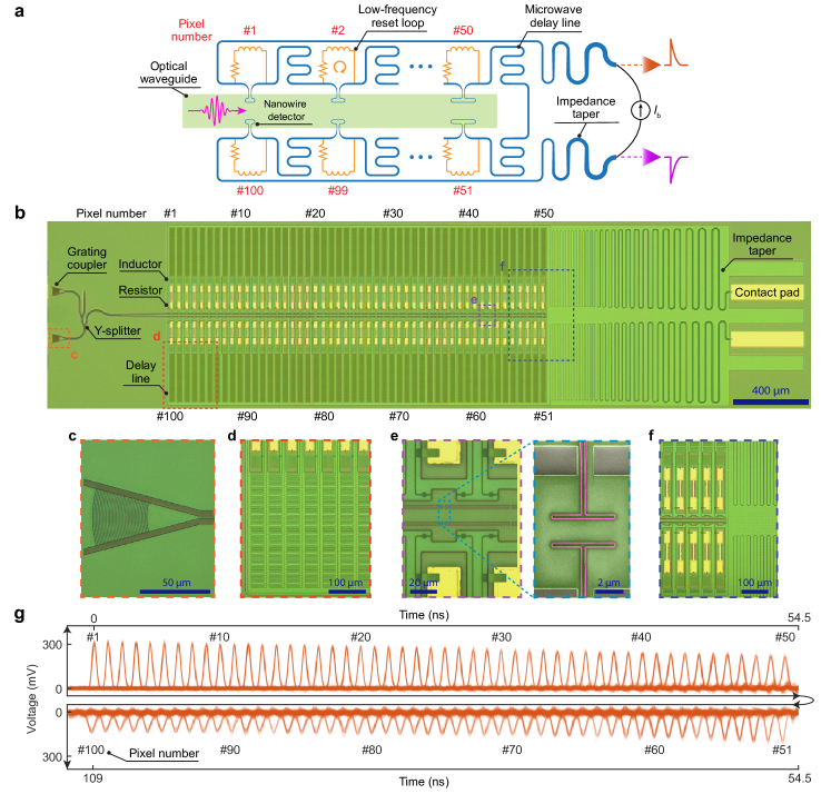
Operation principle of detector. Fig. 1a illustrates the basic operation principle of the spatiotemporal-multiplexed SNSPD array. The incident photons are guided by the waveguide and spatially distributed to the nanowire detector pixels of incremental length integrated atop the waveguide. All the detector pixels are series connected with identical sections of nanosecond-level delay lines embedded between neighboring pixels. Each pixel is shunted by an on-chip inductor and resistor for the local reset of the bias current after firing. The fired pixel generates a pair of positive/negative microwave pulses that propagate along the opposite direction of the high-frequency bus line consisting of the detector pixels and the delay line sections (blue color). The signals are then read out in time sequence using the method of temporal-multiplexing (Fig. 1g). The impedance tapers are attached at both ends of the bus line to match the impedance between the delay lines and the reading electronics, which is critical for minimizing reflections of the readout signals, and thus preserving clear and fast rising/falling edges35, 36. In addition, the presence of the resistively shunted inductors prevents the high-frequency signals entering the low-frequency reset loop (orange color), rendering the readout and reset of the individual detector pixels separated.
One advantage of this device design is that the nanowire detectors, on-chip inductors, microwave delay lines as well as the impedance tapers could be all implemented in a single ultra-thin niobium nitride (NbN) superconducting layer (Fig. 1b-f), thus greatly simplifying the fabrication process. Moreover, a compact design of ultra-slow microwave transmission line based on high-kinetic-inductance NbN nanowires and high-k dielectric layer (see Methods) is employed here instead of bulky optical delay lines for the temporal-multiplexed readout, and thus a high scalability of the detector pixel number is expected. More importantly, this hybrid spatiotemporal-multiplexing scheme enables position resolving capability; that is, in addition to the information of photon number, the readout scheme could also provide position information on the fired detector pixels. This distinct property compared to other conventional PNR detectors makes our detector a highly versatile platform to perform various quantum optics experiments on a chip.
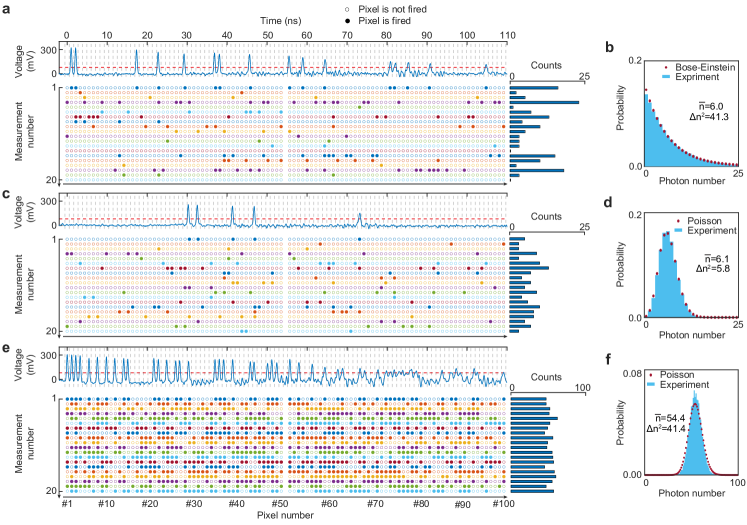
Photon statistics and correlation measurement. We first demonstrate the potential of our detector in quantum optics applications by measuring the photon statistics of thermal and coherent states of light. A fast-speed oscilloscope is used to acquire microwave pulse signals generated by the detector and amplified by low-noise amplifiers (see Supplementary Section I for more details on the measurement setup). One instance of the oscilloscope trace produced by detecting a thermal light source from erbium-doped fiber amplifiers (EDFAs) is shown in Fig. 2a. The presence/absence of the pulses in each time slot, which corresponds to the individual pixel of the detector, can be used to provide the total detected photon number as well as the position information of the fired pixels. The lower panel of Fig. 2a shows 20 measurement sequences as example, and the corresponding total count of photon number in each measurement is attached to the end of each sequence. By collecting a sufficient number of measurements, the histogram of the detected photon numbers can be constructed to get the photon number probability distribution (see Fig. 2b), which follows the Bose-Einstein distribution in excellent agreement. The statistics measurement of a coherent laser source with a similar mean photon number () is shown in Fig. 2c,d and a much higher number () in Fig. 2e,f to showcase the large-dynamic-range PNR capability of our detector. Both traces from the coherent source follow the Poisson distribution, and the counts of photon number fluctuate much less strongly than that of the thermal state due to the lack of photon bunching (also see Supplementary Movies). It is also worth noting that as the total detected photon number increases, the peak-to-background ratio gets deteriorated, particularly for the signals from the latter half part of the pixels. This is due to the accumulated low-frequency background ripples from the fired pixel signals in front, which is also captured in our simulation (Supplementary Section II). To mitigate this problem, we can use both output channels of our detector and separately collect the signals for #1 - #50 and #51 - #100 pixels. In the future upgrade, a higher-permittivity dielectric layer, such as SrTiO337, can be employed to greatly reduce the propagation speed of the microwave signals and thus increase the delay time between neighboring pulse signals to help differentiate them. In addition, more advanced waveform processing schemes38 could be developed in the future, instead of simple pulse peaks counting, to better extract the detection information.
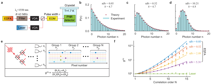
We next use our detector to investigate the effect of pulse width on the quantum statistics of a true thermal light source and compare with that of a coherent counterpart. A simplified schematic of the experimental setup is shown in Fig. 3a (see Supplementary Section I for a complete schematic). The spectrally filtered amplified spontaneous emission from EDFAs and the narrow-bandwidth coherent-state light from a continuous-wave (CW) laser are separately used as the light sources with the variable optical attenuators (VOAs) tuning the light intensity and thus the mean photon number . Both of the sources are followed by the temporal gating through the electro-optic modulator (EOM) to make them pulsed sources. The photon number probability distribution of a thermal light measured by a PNR detector can be described by a negative binomial distribution as 39, 40
| (1) |
where is the full width at half maximum (FWHM) bandwidth of the Lorentzian optical spectral filter 41, and the pulse width. When the time-bandwidth product , Eq. 1 can be reduced to the Bose-Einstein distribution . On the other hand, when , it becomes the Poisson distribution . The spectral filter used in our experiment has a bandwidth of MHz, and the pulse width is tuned by the EOM from 0.24 ns to 100 ns. The photon number probability distributions for are shown in Fig. 3b-d, respectively. It can be clearly seen that the photon statistics gradually transits from the Bose-Einstein distribution to the Poisson distribution, which agrees well with the theoretical calculation by Eq. 1.
With the capability of the position resolving, our detector also allows a convenient and direct measurement of the high-order correlation function , where indicates the ensemble average. The previous conventional measurement of is typically realized by splitting an optical beam into parts and subsequently using single-photon detectors for coincidence counting. By contrast, we can flexibly split 100 pixels of our detector into groups without modifying the experiment setup and count the sum photon number in each group for coincidence measurement, as illustrated in Fig. 3e. The theoretical value of for the EDFA thermal light source can be calculated as 42
| (2) |
where is the gamma function. In the limit of , we have , which agrees with the result of the Bose-Einstein distribution 43. At the other extreme , it follows that , the well-known results of the Poisson distribution. The experimental results for with up to 15 are shown in Fig. 3f, which agree well with the theoretical prediction. When decreases, we can see that the value of increases significantly. By contrast, the value of remains unity when a coherent laser is used as the light source. It should be noted that the measurement of with higher is limited by the slow data acquisition rate of the oscilloscope (30 Hz) used in our experiment, rather than the detector itself, since an exponentially larger sample number is needed to minimize the variance of as increases. A dedicated GHz-level fast pulse counter could be employed in the future experiment to further unlock the performance of our detector.
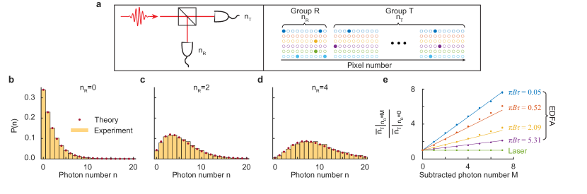
Photon subtraction experiment. We then further investigate the capability of our detector by performing photon subtraction experiment. The conventional photon subtraction entails using a beam-splitter to probabilistically subtract a certain number of photons at the reflection port as shown in Fig. 4a. In our experiment, we split the 100-pixel detector into two groups, i.e., group R and group T, and a splitting ratio is achieved by adjusting the number of pixels in each group. Due to the bunching effect of thermal light, the more photons are subtracted at the reflection port, the higher mean photon number will be detected at the transmission port 44, 45. This effect can be potentially useful for applications, such as quantum-enhanced interferometry 26 and quantum-state engineering 27. Assuming that the input photon number probability distribution can be described by a negative binomial distribution with a mean photon number of , the photon number probability distribution at the transmission port can be described by a second negative binomial distribution , whose mean photon number becomes
| (3) |
where is the subtracted photon number at the reflection port. When , , and , we have , which is the well-known result that the mean photon number of a thermal state at the transmission port will be doubled when a single photon is annihilated at the reflection port of a low-reflection beam-splitter 25. It is also worth noting that the time-bandwidth product of the negative binomial distribution at the transmission port increases from to . Therefore, if the input beam follows the Bose-Einstein statistics with , the photon number distribution at the transmission port will transit to Poisson-like statistics when the annihilated photon number is large. These theoretical predictions agree well with our experimental data as shown in Fig. 4b-d, where respectively. For these measurement, the spectrally filtered EDFA is used as the light source with .
We next investigate the photon number enhancement effect of photon subtraction, and we use
| (4) |
to quantify the photon number enhancement, where is the subtracted photon number at the reflection port. The experimental results of photon number enhancement are shown in Fig. 4e, which illustrates that the photon number enhancement increases linearly as increases. In contrast, there is no enhancement for the coherent light source from the laser, indicating the photon states at the two output ports of the beam-splitter are uncorrelated for a coherent state input25.
Quantum-limited discrimination of photon states. As another application of our detector, we perform quantum-limited discrimination between a thermal state and a coherent state of light 34. Here, the mean photon number of the light source is assumed to be known, but its quantum state, either a thermal state or a coherent state, remains to be discriminated. The minimum possible discrimination error is known as the Helstrom bound 46, which can be computed as , where is the density matrix of a thermal state, is the density matrix of a coherent state, and is the trace distance.
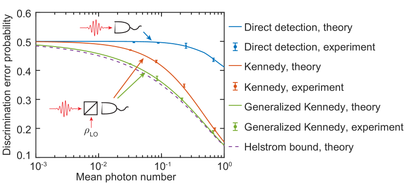
The most straightforward method for discrimination is the direct detection, which entails using a PNR detector to measure the photon number emitted by the source. When photons are measured, its quantum state is discriminated to be a thermal state if . On the other hand, if , the quantum state is discriminated to be a coherent state. The error probability of discrimination can thus be calculated as . However, this method cannot approach the Helstrom bound. The Kennedy receiver can outperform the direct detection by using homodyne detection. A high-transmission beam-splitter () is used to reduce the loss for the signal to be discriminated. The Kennedy detection entails using a local oscillator with a mean photon number of and a relative phase shift with respect to the coherent state light source, whose density matrix can be expressed as with . If the source is a coherent state, the transmission port will present a vacuum state due to the destructive interference. If the source is a thermal state, the state at the transmission port possesses a Laguerre statistics 39, 34 , where is the Laguerre polynomial of order . Therefore, the discrimination error probability is . The Kennedy detection, however, can be further generalized to approach the Helstrom bound by changing to , where the value of depends on and can be computed by numerical optimization 34. In this case, if the source is a coherent state, the detected statistics becomes a Poisson distribution with a mean photon number of . If the source is a thermal state, the detected statistics becomes a Laguerre distribution , and thus the discrimination error probability is . The experimental results measured by the different methods are shown in Fig. 5, which demonstrate that the generalized Kennedy detection closely approaches the Helstrom bound and is the best discrimination method that has been reported 34.
Discussions
In this Article, we have demonstrated a waveguide-integrated and large-dynamic-range PNR detector that employs a hybrid spatiotemporal-multiplexing scheme to read out a 100-pixel SNSPD array. In addition to inheriting all aspects of the excellent performances of single-pixel SNSPDs, this scheme also enables readout of the position information on the fired detector pixels. This distinct functionality makes our detector a versatile platform to perform various quantum optics experiments on a chip at an unprecedented level, such as the photon statistics measurement, the direct measurement of high-order correlation function with up to 15, the photon subtraction experiment with the subtracted photon number up to 4, and the quantum-limited photon state discrimination. In particular, these measurements present a comprehensive characterization of the quantum statistical properties of a true thermal light source for the first time, which is exclusively enabled by the simultaneous availability of high photon number resolution and fast detector response. We believe that our novel detector technology can boost a variety of applications in the near future, such as large-scale Boson sampling 47, photonic quantum computing 48 and quantum metrology 49.
References
- Hadfield 2009 R. H. Hadfield, “Single-photon detectors for optical quantum information applications,” Nat. Photon. 3, 696 (2009).
- Miller et al. 2003 A. J. Miller, S. W. Nam, J. M. Martinis, and A. V. Sergienko, “Demonstration of a low-noise near-infrared photon counter with multiphoton discrimination,” Appl. Phys. Lett. 83, 791 (2003).
- Lita et al. 2008 A. E. Lita, A. J. Miller, and S. W. Nam, “Counting near-infrared single-photons with 95% efficiency,” Opt. Express 16, 3032 (2008).
- Gerrits et al. 2011 T. Gerrits, N. Thomas-Peter, J. C. Gates, A. E. Lita, B. J. Metcalf, B. Calkins, N. A. Tomlin, A. E. Fox, A. L. Linares, J. B. Spring, N. K. Langford, R. P. Mirin, P. G. R. Smith, I. A. Walmsley, and S. W. Nam, “On-chip, photon-number-resolving, telecommunication-band detectors for scalable photonic information processing,” Phys. Rev. A 84 (2011).
- Calkins et al. 2013 B. Calkins, P. L. Mennea, A. E. Lita, B. J. Metcalf, W. S. Kolthammer, A. Lamas-Linares, J. B. Spring, P. C. Humphreys, R. P. Mirin, J. C. Gates, P. G. R. Smith, I. A. Walmsley, T. Gerrits, and S. W. Nam, “High quantum-efficiency photon-number-resolving detector for photonic on-chip information processing,” Opt. Express 21, 22657 (2013).
- Eaton et al. 2022 M. Eaton, A. Hossameldin, R. Birrittella, P. Alsing, C. Gerry, C. Cuevas, H. Dong, and O. Pfister, “Resolving 100 photons and quantum generation of unbiased random numbers,” arXiv:2205.01221 (2022).
- Guo et al. 2017 W. Guo, X. Liu, Y. Wang, Q. Wei, L. F. Wei, J. Hubmayr, J. Fowler, J. Ullom, L. Vale, M. R. Vissers, and J. Gao, “Counting near infrared photons with microwave kinetic inductance detectors,” Appl. Phys. Lett. 110, 212601 (2017).
- Day et al. 2003 P. K. Day, H. G. LeDuc, B. A. Mazin, A. Vayonakis, and J. Zmuidzinas, “A broadband superconducting detector suitable for use in large arrays,” Nature 425, 817 (2003).
- Natarajan et al. 2012 C. M. Natarajan, M. G. Tanner, and R. H. Hadfield, “Superconducting nanowire single-photon detectors: physics and applications,” Supercon. Sci. Technol. 25, 063001 (2012).
- Reddy et al. 2020 D. V. Reddy, R. R. Nerem, S. W. Nam, R. P. Mirin, and V. B. Verma, “Superconducting nanowire single-photon detectors with 98% system detection efficiency at 1550 nm,” Optica 7, 1649 (2020).
- Chang et al. 2021 J. Chang, J. W. N. Los, J. O. Tenorio-Pearl, N. Noordzij, R. Gourgues, A. Guardiani, J. R. Zichi, S. F. Pereira, H. P. Urbach, V. Zwiller, S. N. Dorenbos, and I. E. Zadeh, “Detecting telecom single photons with % system detection efficiency and high time resolution,” APL Photon. 6, 036114 (2021).
- Zhang et al. 2019 W. Zhang, J. Huang, C. Zhang, L. You, C. Lv, L. Zhang, H. Li, Z. Wang, and X. Xie, “A 16-pixel interleaved superconducting nanowire single-photon detector array with a maximum count rate exceeding 1.5 GHz,” IEEE Trans. Appl. Supercond. 29, 1 (2019).
- Korzh et al. 2020 B. Korzh, Q.-Y. Zhao, J. P. Allmaras, S. Frasca, T. M. Autry, E. A. Bersin, A. D. Beyer, R. M. Briggs, B. Bumble, M. Colangelo, G. M. Crouch, A. E. Dane, T. Gerrits, A. E. Lita, F. Marsili, G. Moody, C. Peña, E. Ramirez, J. D. Rezac, N. Sinclair, M. J. Stevens, A. E. Velasco, V. B. Verma, E. E. Wollman, S. Xie, D. Zhu, P. D. Hale, M. Spiropulu, K. L. Silverman, R. P. Mirin, S. W. Nam, A. G. Kozorezov, M. D. Shaw, and K. K. Berggren, “Demonstration of sub-3 ps temporal resolution with a superconducting nanowire single-photon detector,” Nat. Photon. (2020).
- Shibata et al. 2015 H. Shibata, K. Shimizu, H. Takesue, and Y. Tokura, “Ultimate low system dark-count rate for superconducting nanowire single-photon detector,” Opt. Lett. 40, 3428 (2015).
- Zhu et al. 2020 D. Zhu, M. Colangelo, C. Chen, B. A. Korzh, F. N. Wong, M. D. Shaw, and K. K. Berggren, “Resolving photon numbers using a superconducting nanowire with impedance-matching taper,” Nano Lett. 20, 3858 (2020).
- Cahall et al. 2017 C. Cahall, K. L. Nicolich, N. T. Islam, G. P. Lafyatis, A. J. Miller, D. J. Gauthier, and J. Kim, “Multi-photon detection using a conventional superconducting nanowire single-photon detector,” Optica 4, 1534 (2017).
- Natarajan et al. 2013 C. M. Natarajan, L. Zhang, H. Coldenstrodt-Ronge, G. Donati, S. N. Dorenbos, V. Zwiller, I. A. Walmsley, and R. H. Hadfield, “Quantum detector tomography of a time-multiplexed superconducting nanowire single-photon detector at telecom wavelengths,” Opt. Express 21, 893 (2013).
- Divochiy et al. 2008 A. Divochiy, F. Marsili, D. Bitauld, A. Gaggero, R. Leoni, F. Mattioli, A. Korneev, V. Seleznev, N. Kaurova, O. Minaeva, G. Gol'tsman, K. G. Lagoudakis, M. Benkhaoul, F. Lévy, and A. Fiore, “Superconducting nanowire photon-number-resolving detector at telecommunication wavelengths,” Nat. Photon. 2, 302 (2008).
- Cheng et al. 2013 R. Cheng, H. Yin, J. Liu, T. Li, H. Cai, Z. Xu, and W. Chen, “Photon-number-resolving detector based on superconducting serial nanowires,” IEEE Trans. Appl. Supercond. 23, 2200309 (2013).
- Mattioli et al. 2016 F. Mattioli, Z. Zhou, A. Gaggero, R. Gaudio, R. Leoni, and A. Fiore, “Photon-counting and analog operation of a 24-pixel photon number resolving detector based on superconducting nanowires,” Opt. Express 24, 9067 (2016).
- Schmidt et al. 2019 E. Schmidt, E. Reutter, M. Schwartz, H. Vural, K. Ilin, M. Jetter, P. Michler, and M. Siegel, “Characterization of a photon-number resolving SNSPD using poissonian and sub-Poissonian light,” IEEE Trans. Appl. Supercond. 29, 1 (2019).
- Wollman et al. 2019 E. E. Wollman, V. B. Verma, A. E. Lita, W. H. Farr, M. D. Shaw, R. P. Mirin, and S. W. Nam, “Kilopixel array of superconducting nanowire single-photon detectors,” Opt. Express 27, 35279 (2019).
- Hanbury Brown and Twiss 1956 R. Hanbury Brown and R. Q. Twiss, “Correlation between photons in two coherent beams of light,” Nature 177, 27 (1956).
- Bennink et al. 2002 R. S. Bennink, S. J. Bentley, and R. W. Boyd, ““Two-photon” coincidence imaging with a classical source,” Phys. Rev. Lett. 89, 113601 (2002).
- Zavatta et al. 2008 A. Zavatta, V. Parigi, M. Kim, and M. Bellini, “Subtracting photons from arbitrary light fields: experimental test of coherent state invariance by single-photon annihilation,” New J. Phys. 10, 123006 (2008).
- Rafsanjani et al. 2017 S. M. H. Rafsanjani, M. Mirhosseini, O. S. Magaña-Loaiza, B. T. Gard, R. Birrittella, B. Koltenbah, C. Parazzoli, B. A. Capron, C. C. Gerry, J. P. Dowling, et al., “Quantum-enhanced interferometry with weak thermal light,” Optica 4, 487 (2017).
- Magaña-Loaiza et al. 2019 O. S. Magaña-Loaiza, R. d. J. León-Montiel, A. Perez-Leija, A. B. U’Ren, C. You, K. Busch, A. E. Lita, S. W. Nam, R. P. Mirin, and T. Gerrits, “Multiphoton quantum-state engineering using conditional measurements,” npj Quantum Inform. 5, 80 (2019).
- Goodman 2015 J. W. Goodman, Statistical optics (John Wiley & Sons, 2015).
- Martienssen and Spiller 1964 W. Martienssen and E. Spiller, “Coherence and fluctuations in light beams,” Am. J. Phys. 32, 919 (1964).
- Zhai et al. 2005 Y.-H. Zhai, X.-H. Chen, D. Zhang, and L.-A. Wu, “Two-photon interference with true thermal light,” Phys. Rev. A 72, 043805 (2005).
- Liu et al. 2014 X.-F. Liu, X.-H. Chen, X.-R. Yao, W.-K. Yu, G.-J. Zhai, and L.-A. Wu, “Lensless ghost imaging with sunlight,” Opt. Lett. 39, 2314 (2014).
- Tan et al. 2014 P. K. Tan, G. H. Yeo, H. S. Poh, A. H. Chan, and C. Kurtsiefer, “Measuring temporal photon bunching in blackbody radiation,” Astrophys. J. Lett. 789, L10 (2014).
- Deng et al. 2019 Y.-H. Deng, H. Wang, X. Ding, Z.-C. Duan, J. Qin, M.-C. Chen, Y. He, Y.-M. He, J.-P. Li, Y.-H. Li, et al., “Quantum interference between light sources separated by 150 million kilometers,” Phys. Rev. Lett. 123, 080401 (2019).
- Habif et al. 2021 J. L. Habif, A. Jagannathan, S. Gartenstein, P. Amory, and S. Guha, “Quantum-limited discrimination of laser light and thermal light,” Opt. Express 29, 7418 (2021).
- Zhao et al. 2017 Q.-Y. Zhao, D. Zhu, N. Calandri, A. E. Dane, A. N. McCaughan, F. Bellei, H.-Z. Wang, D. F. Santavicca, and K. K. Berggren, “Single-photon imager based on a superconducting nanowire delay line,” Nat. Photon. 11, 247 (2017).
- Cheng et al. 2019a R. Cheng, C.-L. Zou, X. Guo, S. Wang, X. Han, and H. X. Tang, “Broadband on-chip single-photon spectrometer,” Nat. Commun. 10, 1 (2019a).
- Santavicca et al. 2021 D. F. Santavicca, M. Colangelo, C. R. Eagle, M. P. Warusawithana, and K. K. Berggren, “50 Ohm transmission lines with extreme wavelength compression based on superconducting nanowires on high-permittivity substrates,” Appl. Phys. Lett. 119, 252601 (2021).
- Zhu et al. 2018 D. Zhu, Q.-Y. Zhao, H. Choi, T.-J. Lu, A. E. Dane, D. Englund, and K. K. Berggren, “A scalable multi-photon coincidence detector based on superconducting nanowires,” Nature Nanotechnology 13, 596 (2018).
- Karp et al. 2013 S. Karp, R. M. Gagliardi, S. E. Moran, and L. B. Stotts, Optical channels: fibers, clouds, water, and the atmosphere (Springer Science & Business Media, 2013).
- Agarwal 1992 G. Agarwal, “Negative binomial states of the field-operator representation and production by state reduction in optical processes,” Phys. Rev. A 45, 1787 (1992).
- Mandel and Wolf 1962 L. Mandel and E. Wolf, “The measures of bandwidth and coherence time in optics,” Proc. Phys. Soc. Lond. 80, 894 (1962).
- Zhai et al. 2013 Y. Zhai, F. E. Becerra, B. L. Glebov, J. Wen, A. E. Lita, B. Calkins, T. Gerrits, J. Fan, S. W. Nam, and A. Migdall, “Photon-number-resolved detection of photon-subtracted thermal light,” Opt. Lett. 38, 2171 (2013).
- Stevens et al. 2010 M. J. Stevens, B. Baek, E. A. Dauler, A. J. Kerman, R. J. Molnar, S. A. Hamilton, K. K. Berggren, R. P. Mirin, and S. W. Nam, “High-order temporal coherences of chaotic and laser light,” Opt. Express 18, 1430 (2010).
- Parigi et al. 2007 V. Parigi, A. Zavatta, M. Kim, and M. Bellini, “Probing quantum commutation rules by addition and subtraction of single photons to/from a light field,” Science 317, 1890 (2007).
- Barnett et al. 2018 S. M. Barnett, G. Ferenczi, C. R. Gilson, and F. C. Speirits, “Statistics of photon-subtracted and photon-added states,” Phys. Rev. A 98, 013809 (2018).
- Helstrom 1976 C. W. Helstrom, Quantum detection and estimation theory (Academic Press, 1976).
- Tillmann et al. 2013 M. Tillmann, B. Dakić, R. Heilmann, S. Nolte, A. Szameit, and P. Walther, “Experimental boson sampling,” Nat. Photon. 7, 540 (2013).
- Kok et al. 2007 P. Kok, W. J. Munro, K. Nemoto, T. C. Ralph, J. P. Dowling, and G. J. Milburn, “Linear optical quantum computing with photonic qubits,” Rev. Mod. Phys. 79, 135 (2007).
- Matthews et al. 2016 J. C. Matthews, X.-Q. Zhou, H. Cable, P. J. Shadbolt, D. J. Saunders, G. A. Durkin, G. J. Pryde, and J. L. O’Brien, “Towards practical quantum metrology with photon counting,” npj Quantum Inform. 2, 1 (2016).
- Cheng et al. 2019b R. Cheng, S. Wang, and H. X. Tang, “Superconducting nanowire single-photon detectors fabricated from atomic-layer-deposited NbN,” Applied Physics Letters 115, 241101 (2019b).
Acknowledgments
This work is funded by the National Science Foundation (NSF) through ERC Center for Quantum Networks (CQN) grant EEC-1941583. We acknowledge early funding support for this project from DARPA DETECT program through an ARO grant (No. W911NF-16-2-0151) and NSF EFRI grant (EFMA-1640959). The authors would like to thank Dr. Yong Sun, Sean Rinehart, Kelly Woods, and Dr. Michael Rooks for their assistance provided in the device fabrication. The fabrication of the devices was done at the Yale School of Engineering & Applied Science (SEAS) Cleanroom and the Yale Institute for Nanoscience and Quantum Engineering (YINQE).
Author contributions
R.C., Y.Z., and H.X.T. conceived the idea and experiment; R.C. designed and fabricated the devices; R.C., Y.Z., S.W., M.S., and T.T. performed the measurements; R.C. and Y.Z. analyzed the data. R.C., Y.Z. and H.X.T. wrote the manuscript with inputs from all authors. H.X.T. supervised the project.
Competing interests
The authors declare no competing interests.
Additional information
Supplementary information is available in the online version of the paper.
Correspondence and requests for materials should be addressed to H.X.T.
Methods
Device fabrication. The fabrication of the device involves six steps of high-resolution () e-beam lithography (EBL) and following etching or deposition/lift-off process. (1) Alignment markers are pre-fabricated on top of a 4-inch 330-thick LPCVD-Si3N4 / -thick thermal oxide / Si wafer by standard double-layer polymethyl methacrylate (PMMA) patterning process, e-beam evaporation of 10 nm Cr / 100 nm Au layers, and following lift-off in acetone. (2) High-uniformity 8 nm-thick NbN superconducting thin film is deposited by atomic layer deposition (ALD)50 afterwards and followed by the e-beam patterning of the negative-tone 6% hydrogen silsesquioxane (HSQ) resist. It is worth noting that the spinning and patterning of HSQ resist right after the fresh NbN film deposition is critical in maintaining excellent adhesion of the resist. (3) In the third EBL step, the electrode pads and contact pads for the on-chip resistors are defined by another double-layer PMMA patterning, e-beam evaporation of 5 nm Cr / 25 nm Au, and following lift-off process. Later, the HSQ pattern is transferred to the NbN layer in a timed reactive-ion etching (RIE) step employing tetrafluoromethane (CF4) chemistry, which defines the nanowire detector pixels, delay lines, on-chip inductors, and impedance tapers. (4) In the fourth EBL step, we pattern the positive-tone AR-P 6200 (CSAR 62) resist for the photonic microstructures, including gratings couplers, Y-splitters, and waveguides. The patterns are then transferred to the Si3N4 film via carefully timed RIE in fluoroform (CHF3). The remaining resist is removed by gentle oxygen plasma and hot N-methylpyrrolidone (NMP). (5) In the fifth EBL step, we define the on-chip resistors by patterning double-layer PMMA and e-beam evaporation of 80 nm Cr / 5 nm Au with lift-off process. (6) Lastly, the 80 nm-thick alumina (AlOx) dielectric spacing layer and 100 nm-thick aluminum (Al) top ground layer are fabricated by double-layer PMMA patterning, e-beam evaporation, and lift-off for making the low-speed microwave transmission line. The remaining HSQ mask on top of the NbN delay line area is removed by 1:100 diluted hydrofluoric (HF) acid after opening the PMMA window (lighter area in Fig. 1b) and before the deposition of AlOx/Al layers. The resulting devices is shown in Fig. 1b-f, and additional device images as well as the fabrication yield are presented in Supplementary Section III.
Device design. As shown in Fig. 1b, the photons are launched into the Si3N4 waveguide from a fiber through the input grating coupler. The waveguide is then split into two branches, one of which is attached to the output grating coupler for power calibration and alignment, while the other one is adiabatically tapered from 1.2 m width to 8 m and then connected to a series of 100 NbN nanowire detector pixels placed atop the waveguide. All the detector pixels are made of hairpin-shaped 80 nm-wide NbN nanowires that guarantee saturated internal efficiency at 1550 nm telecommunication wavelength (see Supplementary Section V). Each of the nanowire is shunted by a 5 m-wide and 50 m-long Cr/Au on-chip resistor (corresponding to 60 resistance at 1.7 K) and an inductor made of a 400 nm-wide NbN meander wire (corresponding to 200 nH inductance). All the nanowires are series-connected with long meandered 800 nm-wide NbN delay lines embedded in between, as visualized in Fig. 1b. Both ends of the nanowire-detector-delay-line chain are connected to the impedance tapers consisting of meandered NbN wires with gradually varying widths from 800 nm to 9.2 m, which follow the Klopfenstein design to match the impedance between the delay lines (hundreds of ohms) and the external reading electronics (50 ). The total length of each impedance taper is , which allows <50 MHz lower cut-off frequency. The long impedance tapers here play an important role in preserving the fast-rising edges and clear shapes of the photon-excited detector pulses by suppressing multiple reflections between the device and external readout electronics. At the ends of the impedance tapers, the microstrip lines are converted to coplanar waveguides (CPWs) to match the modes of ground-signal-ground (GSG) RF probes.
By engineering the length and the distance of the nanowire from the edge of the waveguide, we could tune the photon absorption efficiency of each nanowire and thus ensure the input photons are evenly distributed over the detector pixels. In the etched clearance area for the waveguide, a 1.3 m-wide bridges are designed for the connection of each nanowire detector to the delay line sections that are positioned outside the waveguide area (Fig. 1e). The 3D finite-difference time-domain (FDTD) simulation study shows that the total scattering loss induced by 100 of such bridges is lower than 0.3 dB. We further confirm the results by investigating the quality factors of Si3N4 racetrack resonators with varying number of bridges embedded in the straight waveguide sections.
The parts of NbN delay lines and the impedance tapers are capped by a high-dielectric-constant (high-k) AlOx layer and top metal ground made of Al layer (lighter area in Fig. 1b), which helps significantly slow down the propagation speed of the photon-excited microwave signals, thereby enabling a very compact device design and also reducing the cross-talk between the transmission lines. Due to the high kinetic inductance of the superconducting wires made of NbN thin film and the high capacitance introduced by the thin high- layer, the propagation speed could be achieved as low as 1.07% of (vacuum speed of light), despite the significantly wide delay lines compared to the nanowire detector. Each delay line section is designed to be 3.4 mm long and introduces a 1.09 ns propagation time delay between neighboring detector pixels (Fig. 1g).
Device characterization. The sample chip containing tens of detector devices is mounted on a 3-axis stack of stages (Attocube) inside a low-vibration closed-cycle refrigerator (Cryomech) and cooled down to base temperature. We drive the stages to move the sample chip and make the electrode contact with a multi-channel RF probe, which is used for DC-biasing the detector device and reading out the photon-excited microwave pulses. In the meantime, the grating couplers are aligned to the single-mode fiber array by optimizing the optical transmission through the device (see Fig. 1 and Supplementary Section V). The photons are coupled into the waveguide from one of the fiber through the input grating coupler, while parts of them are output from the other calibration grating coupler, collected with another optical fiber in the same fiber array, and finally detected with a calibrated room-temperature photodetector. This cryogenic optical setup not only guarantees multiple optical and RF channels input/output, but also allows for measurements on multiple devices in a single round of cool-down.
The pulsed coherent light source is generated by gating a tunable continuous-wave (CW) laser (New Focus 6427 Vidia-Discrete) with the cascaded electro-optic modulators (EOMs) and acoustic-optic modulator (AOM), which guarantees sub-ns narrow pulse width combined with >100 dB extinction ratio to efficiently suppress the background photons. The thermal light source is generated by employing the same gating method but with the EDFA/narrow-bandwidth spectral filter chain to replace the CW laser part. A more detailed description on the measurement setup can be found in Supplementary Section I.
Data availability
The data that support the plots within this paper and other findings of this study are available from the corresponding author upon reasonable request.