Tunable spin and valley excitations of correlated insulators in -valley moiré bands
Abstract
Moiré superlattices formed from transition metal dichalcogenides (TMDs) support a variety of quantum electronic phases that are highly tunable using applied electromagnetic fields. While the valley degree of freedom affects optoelectronic properties in the constituent TMDs, it has yet to be fully explored in moiré systems. Here, we establish twisted double bilayer WSe2 as an experimental platform to study electronic correlations within -valley moiré bands. Through local and global electronic compressibility measurements, we identify charge-ordered phases at multiple integer and fractional moiré fillings. By measuring the magnetic field dependence of their energy gaps and the chemical potential upon doping, we reveal spin-polarized ground states with spin polaron quasiparticle excitations. In addition, an applied displacement field induces a metal-insulator transition driven by tuning between - and -valley moiré bands. Our results demonstrate control over the spin and valley character of the correlated ground and excited states in this system.
I Introduction
Control over the electronic band structure and internal quantum degrees of freedom in solid state materials is highly desirable to engineer novel functionality. Moiré van der Waals heterostructures, in which an interlayer twist and/or mismatch between lattice constants produces a long-wavelength spatial modulation, have attracted great interest due to their ability to host flat bands in which electronic interactions dominate over kinetic energy andrei_graphene_2020 ; balents_superconductivity_2020 ; kennes_moire_2021 . Moiré superlattices engineered from semiconducting transition metal dichalcogenides (TMDs) are a particularly flexible platform for investigating correlated electronic states because the resulting physics can be tuned by adjusting TMD composition and stacking orientation, while flat bands emerge without stringent constraints on twist angle wu_hubbard_2018 ; zhang_moire_2020 ; wu_topological_2019 ; angeli__2021 ; zhang_electronic_2021 . Multiple homo- and heterobilayer systems have been explored to date, revealing correlation-driven charge transfer and/or Mott insulating states at integer moiré fillings regan_mott_2020 ; tang_simulation_2020 ; wang_correlated_2020 ; li_charge-order-enhanced_2021 ; li_quantum_2021 ; xu_tunable_2022 and a series of generalized Wigner crystals at fractional fillings regan_mott_2020 ; xu_correlated_2020 ; chu_nanoscale_2020 ; li_charge-order-enhanced_2021 ; li_imaging_2021 ; huang_correlated_2021 ; tang_dielectric_2022 . These correlated electronic states are often strongly tuned by applied gate voltages and magnetic fields, which can favor different many-body ground states and/or modify the underlying single-particle bands ghiotto_quantum_2021 ; li_continuous_2021 ; li_quantum_2021 ; tang_dielectric_2022 ; zhang_pomeranchuk_2022. As a result, the TMD platform is an ideal venue for quantum simulation and study of the Hubbard model, which is thought to capture the essential physics of conventional strongly correlated materials kennes_moire_2021 ; wu_hubbard_2018 ; tang_simulation_2020 ; pan_quantum_2020 . This has motivated careful measurement of the spin ordering of the ground states hu_competing_2021 ; xu_tunable_2022 ; wang_light-induced_2022 ; tang_evidence_2023 . However, experimental studies have primarily focused on low magnetic fields, and little is known about the nature of the lowest energy excitations or their field dependence.
The valley degree of freedom, which captures the momentum of the low-energy states, also plays an important role in TMDs, and the valley character of the moiré bands derives from that of the constituent TMDs angeli__2021 ; magorrian_multifaceted_2021 ; vitale_flat_2021 ; xian_realization_2021 . If the moiré bands are localized around the -valley, then these bands will be spin degenerate but have no valley degeneracy. This presents a qualitatively distinct physical system relative to -valley TMDs, which have two degenerate spin-valley-locked bands angeli__2021 ; wang_correlated_2020 . Due to the structure of TMDs, there are also two distinct stackings of their moiré superlattices shabani_deep_2021 . Twisted -valley moiré TMD systems with AA (i.e. near 3R) stacking are predicted to realize effective Hubbard models in honeycomb and Kagome geometries angeli__2021 ; zhang_electronic_2021 ; xian_realization_2021 . AB (i.e. near 2H) stacked -valley systems realize a triangular lattice, which can have flatter bands due to the larger effective mass at , enhancing the importance of interactions. In untwisted TMDs, increasing the number of layers shifts the valence band edge from to mak_atomically_2010 ; xu_spin_2014 , and tuning the relative populations of these two valleys with applied electric field was demonstrated in magnetotransport measurements in trilayer WSe2 movva_tunable_2018 . However, few experimental realizations of -valley moiré systems have been reported, and their electronic properties are poorly characterized. The interplay of -valley-tunable physics in the context of moiré bands also remains an open question in experiments.
Here we study magnetic and electric displacement field dependence of correlated insulators in -valley hole moiré bands in AB-stacked twisted double bilayer WSe2 (tdWSe2; Fig. 1a). We measure the chemical potential and inverse electronic compressibility both locally using a scanning single-electron transistor (SET) and globally in dual gated devices. Our measurements reveal charge-ordered states at integer and fractional moiré filling factors and , where corresponds to one hole per moiré unit cell. The measured gaps grow linearly with perpendicular magnetic field in the low-field regime, indicating spin-polarized ground states. The gap saturates at high fields, and the behavior of the chemical potential in its vicinity provides evidence that itinerant spin polarons, bound states of added electrons and spin-flipped holes, are the lowest energy charged excitations davydova_itinerant_2022 . The thermodynamic energy gaps at integer fillings decrease monotonically with electric displacement field, driven by a single-particle band crossing between the lowest energy and moiré bands. Our experiments establish a new approach to engineer -valley moiré bands and fully characterize the real- and momentum-space localization of the correlated ground states and their excitations.
II -valley moiré bands in tdWSe2
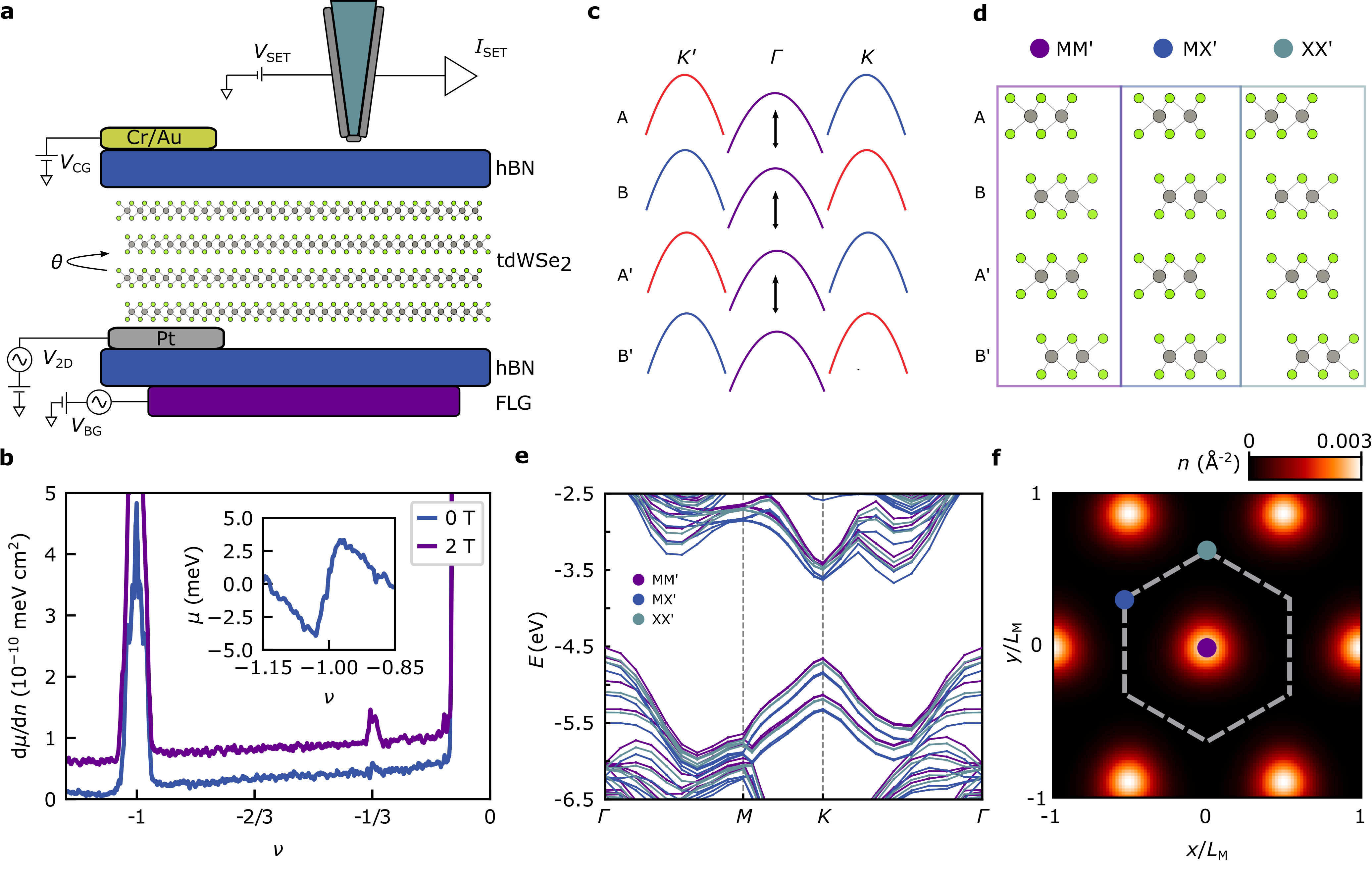
We focus first on local measurements using a scanning SET, schematically illustrated in Fig. 1a. The SET simultaneously and independently probes two related thermodynamic quantities, the inverse electronic compressibility d/d at low a.c. frequency and the chemical potential on d.c. timescales (Methods). This technique mitigates the problem of large contact/intrinsic resistance that often complicates electrical measurements in TMD moiré materials regan_mott_2020 ; li_charge-order-enhanced_2021 . In Sample S1 (Fig. 1b), we observe a pronounced incompressible state at 1012 cm-2, which we identify with . A weaker incompressible peak is also evident at , and it becomes prominent in a small applied out of plane magnetic field . Both of these features are generically present across a wide range of spatial locations (Supplementary Sec. 1), and from the densities at which they occur, we extract a twist angle of (Methods). The corresponding thermodynamic gap , defined as the step size in at filling , can be determined from the d.c. measurement of chemical potential (Fig. 1b, inset), yielding meV at (Supplementary Sec. 2). We also measured a similar gap at in a second device (Sample S2) with a smaller twist angle of . Both samples show very little () twist angle variation (Supplementary Sec. 1), so we focus on a single spatial location in each device throughout the main text.
As a first step toward understanding the correlated states, we consider the low energy valence band structure at the single-particle level in AB-stacked tdWSe2. Due to strong spin-orbit coupling in WSe2, interlayer coupling between adjacent layers is suppressed by spin mismatch at the the and valleys zhu_giant_2011 ; xu_spin_2014 ; shi_bilayer_2022 . At the point, there is no such barrier to interlayer tunneling and hybridization can increase the valence band energy at as the layer number increases (Fig. 1c). This has been both predicted in theoretical calculations and observed in experiments in few-layer WSe2 liu_electronic_2015 ; wilson_determination_nodate ; movva_tunable_2018 . Additionally, a previous ARPES measurement of tdWSe2 found the valence band maximum to occur at rather than an_interaction_2020 .
We confirm this picture by performing density functional theory (DFT) calculations at zero displacement field on the high symmetry stackings of tdWSe2 (Fig. 1d, Methods). The respective band structures (Fig. 1e) demonstrate that the valence band maximum occurs at the valley in the stacking and is separated by roughly 100 meV from the energies at other stackings. Using the energies obtained from DFT, we develop an effective continuum model describing moiré bands from both and valley bands involving all four layers (Supplementary Sec. 3). This continuum model also allows us to later incorporate the effect of a perpendicular displacement field as an effective layer potential difference. The combination of large effective mass at and strong moiré potential results in a very flat first moiré band which is well localized at the sites (Fig. 1f, Supplementary Sec. 3). Due to the two-fold spin degeneracy of the moiré bands, the experimentally observed gap at must be driven by interactions. Measurements as a function of displacement field, discussed in detail below, suggest that the lowest-energy charge excitations at populate a moiré band at the -valley. Combining this experimental finding with first-principles calculations that take into account Coulomb and charge transfer energies, we find that this -valley moiré band will be well-localized at in real space (Supplementary Sec. 3).
III Magnetic field dependence of charge-ordered states
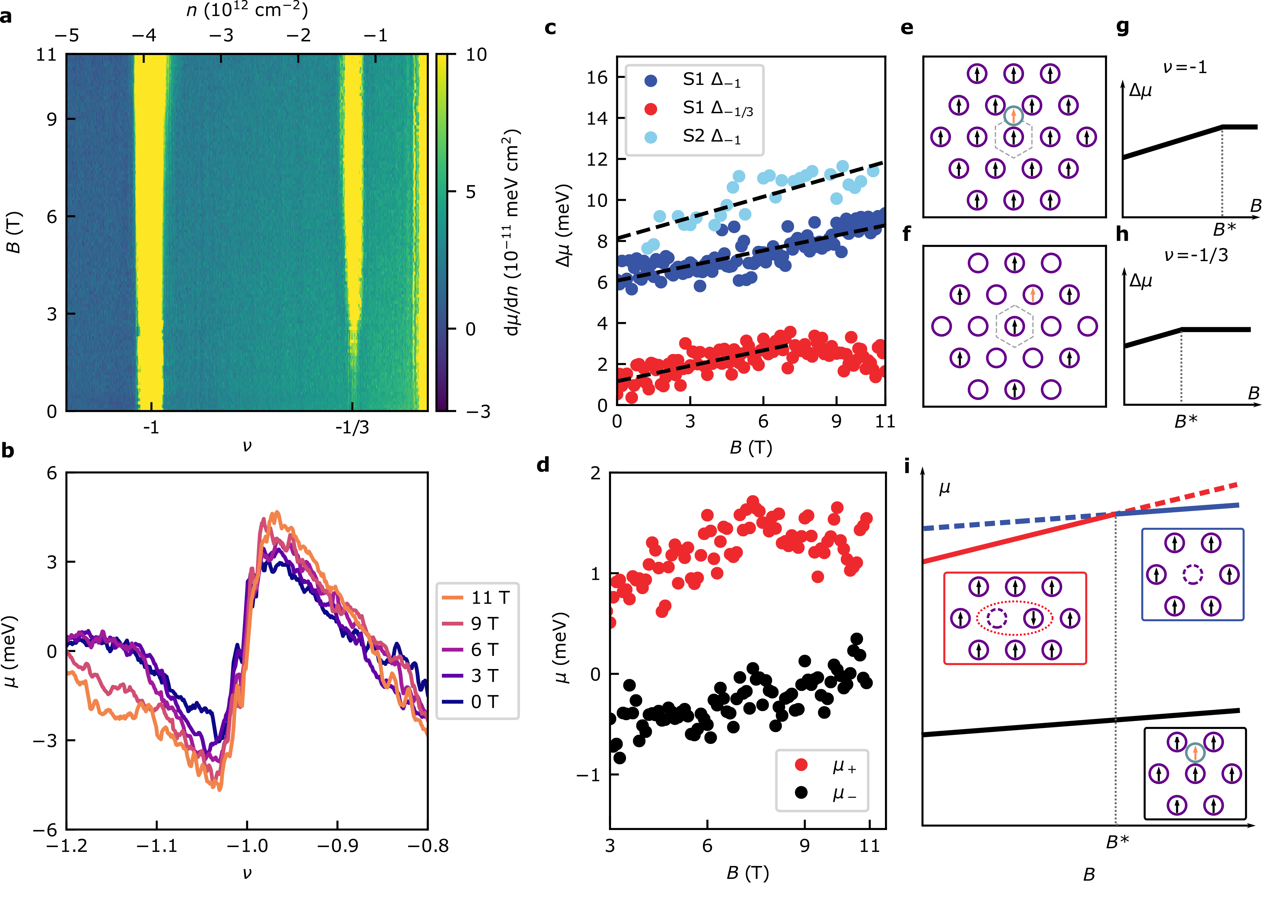
The evolution of the charge gaps in a perpendicular magnetic field clarifies the spin physics of the correlated insulating ground states and their charged excitations. Both the and gaps grow in a magnetic field (Fig. 2a-b, Supplementary Sec. 2). grows linearly with throughout the experimentally accessible field range, whereas increases up to T before saturating or decreasing slightly at high fields (Fig. 2c). The regime of linear growth reflects Zeeman energy shifts, indicating that the insulating state is spin-polarized and a spin-flip is involved in the lowest energy particle-hole excitation. This is consistent with prior reports of small exchange coupling in moiré systems, such that a small magnetic field is sufficient to polarize the spins in the gapped ground state tang_simulation_2020 . However, we note that the observation of spin-polarized correlated insulators in a magnetic field differs from reports in twsited bilayer WSe2 ghiotto_quantum_2021 . We assume that the insulating state at is a generalized Wigner crystal, so that both of these states realize triangular lattices in real space (Fig. 2e-f).
The saturating gap at indicates a change in the nature of the excitations at high fields. The thermodynamic gap that we measure is equivalent to the particle-hole excitation energy (Supplementary Sec. 4), and therefore requires us to take into account the magnetic field dependence of the excitations both above and below the gap. One possible explanation is that the lowest energy excitation just below the gap is the addition of a hole of opposite spin at low fields, before Zeeman coupling overcomes exchange to favor adding an aligned hole (Supplementary Sec. 5). In this scenario, the excitation above the gap would be the removal of a single hole, independent of magnetic field.
However, recent theory suggests that more exotic spin polaron quasiparticles may be relevant in a half-filled triangular lattice with a spin-polarized ground state davydova_itinerant_2022 . In this second scenario, the excitation below the gap remains the same at all magnetic fields: addition of an aligned hole at an interstitial (charge-transfer) site (Fig. 2i, black inset). Above the gap, the lowest energy excitation below a critical field involves removing a hole and flipping the spin of an adjacent remaining hole on the lattice, creating an itinerant spin polaron quasiparticle (Fig. 2i, red inset) with effective spin . At magnetic fields exceeding , formation of spin polarons is no longer favored due to Zeeman coupling, and the excitation involves removing a bare hole without flipping any other spins (Fig. 2i, blue inset).
To distinguish between these two pictures, both of which predict a saturation of the gap size, we examine the behavior of the chemical potential as we dope away from the charge ordered state. The first scenario would involve a sharp change in the behavior of the chemical potential below the gap (Supplementary Sec. 5). In contrast, the spin polaron scenario would lead to a change in the chemical potential above the gap, : the theoretical chemical potentials for each excitation are shown in Fig. 2i. In Fig. 2d, we show the magnetic field dependence of the experimentally measured chemical potentials and on either side of the gap (Supplementary Sec. 6). While is completely smooth, changes slope sharply around T, consistent only with the spin polaron picture. We therefore conclude that spin polarons are favored at lower hole doping of the insulator below T, providing the first experimental evidence for these composite quasiparticles.
Theoretically, the critical field scales with the hopping on the triangular lattice davydova_itinerant_2022 . Because the sites are closer together for the insulating state at as compared to the generalized Wigner crystal at , the effective will be higher at , such that the crossover field at is inaccessible in our measurements (Fig. 2e-h). Nonetheless, the observed chemical potential evolution on either side of the gap suggests that the spin polaron excitations are relevant there as well (Supplementary Sec. 6).
Finally, we fit the linear growth of the and gaps in a magnetic field with an effective -factor , defined by . In Sample S1, both gaps at and exhibit a similar effective -factor . In Sample S2, we measure a larger for . These values exceed the bare spin contribution that we would expect from the predicted excitation (Supplementary Sec. 4). At , this likely reflects additional contributions from orbital effects aivazian_magnetic_2015 ; movva_tunable_2018 ; gustafsson_ambipolar_2018 . At , we do not expect an orbital component as the gap does not involve any change in moiré band. However, exchange enhancement of has been observed previously in TMDs and two-dimensional electron gases (2DEGs), particularly at low densities, and the observation of at likely stems from that effect gustafsson_ambipolar_2018 ; movva_density-dependent_2017 ; nicholas_exchange_1988 ; tutuc_spin_2002 .
Away from the gapped states, our measurements also reveal regions with negative d/d. This is visible on either side of the gap at in Fig. 2b, and occurs over a wide range of fillings, a signature of strong Coulomb interactions eisenstein_negative_1992 ; eisenstein_compressibility_1994 . This negative compressibility can be understood through consideration of exchange interactions, which are sizable relative to the density of states contribution to in this system (see Supplementary Secs. 7-8 for further discussion). The overall size of negative compressibility increases in a magnetic field, suggesting paramagnetism through much of the density range outside of the correlated insulator gaps.
IV Displacement field tuning of moiré bands
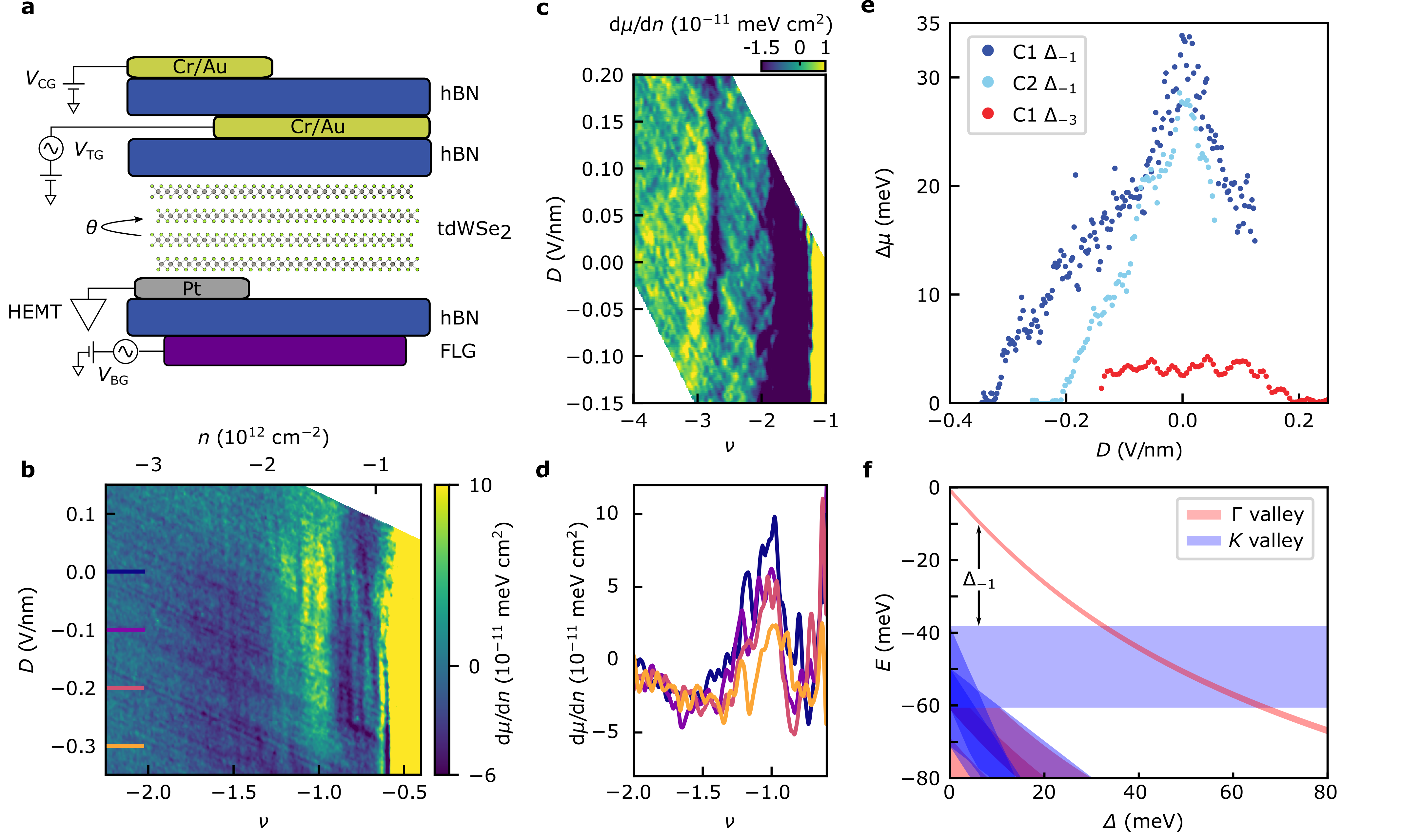
We next discuss the displacement field dependence of the correlated insulators, which has previously been shown to induce particularly strong effects in homobilayers where states are extended across layers wang_correlated_2020 ; xu_tunable_2022 . To study this thermodynamically in tdWSe2, we fabricate samples with top and bottom gates and measure the sample-gate capacitance as a function of moiré filling factor and electrical displacement field (Fig. 3a, Methods). We studied two samples (C1 and C2) using this technique, with twist angles of and , respectively. As hole density is increased beyond the mobility edge at , a broad region of negative is present before an insulating gap appears at (Fig. 3b, Supplementary Sec. 9). In both samples, reaches a maximum around 30 meV at and closes monotonically with , disappearing around V/nm (Fig. 3d-e). Despite the large apparent difference in gap sizes, this is largely consistent with the SET measurements, where the single gate geometry leads to a nonzero displacement field (Supplementary Sec. 10). Qualitatively similar behavior occurs at (Fig. 3c), whose gap also vanishes at high displacement field but shows a plateau within the signal to noise for V/nm (Fig. 3e)
Previous works in TMD moiré systems have shown that displacement fields can drive a continuous metal-insulator transition by changing the bandwidth of the underlying moiré bands ghiotto_quantum_2021 ; li_continuous_2021 . In those experiments, the transport gap closes over a small range of displacement field ( V/nm) and does not vary strongly with outside of that range. At in our device, the gap closes smoothly over a much larger range of , and changes continuously all the way to . Simultaneously, our continuum modeling suggests the bandwidth of the moiré bands should be largely unaffected by displacement field.
Instead, our measurements and modeling are consistent with the lowest energy moiré band switching from to at sufficient layer potential imbalance (Fig. 3f, Supplementary Sec. 5). Because the gap is set by the charge transfer excitation from to moiré bands, tuning the relative moiré band energies leads to a continual change in the measured gap. Past the critical displacement field where the -valley moiré band crosses, we do not measure an incompressible state at , likely due to band overlap and/or the greater dispersion of the -valley moiré band. The measured gap sizes and critical displacement field at show weak dependence on twist angle: Samples C1 and C2 have twist angles that differ by about but the extracted gap at is similar across devices. This is because the gap size and displacement field dependence is largely set by the relative energy of the valence band edge of and at the band edge (Fig. 1e) and the effect that displacement field has on those energies, rather than details of the moiré band structure itself. The continuous closing of the gap from its maximum at provides experimental evidence that the lowest energy moiré bands at low displacement fields are from the -valley and that even at , the lowest energy excitations at are to -valley moiré bands.
V Outlook
In conclusion, we show prominent effects of electronic interactions in -valley moiré bands over a wide range of parameter space in tdWSe2. The correlated insulators we observe exhibit distinct magnetic and displacement field dependence compared to reports of other TMD moiré superlattices. Measurements of the chemical potential upon doping these charge-ordered states reveal evidence for spin polaron quasiparticle excitations. Together, this demonstrates that AB-stacked -valley moiré TMDs realize novel parameter regimes of a mesoscopic triangular lattice model. Our work also suggests a clear path toward engineering low-disorder -valley bands to look at new lattice geometries including honeycomb, Kagome, and anisotropic multi-orbital generalizations of the Hubbard model angeli__2021 , as well as spontaneous ferroelectric states zhang_electronic_2021 . A relatively modest displacement field is sufficient to tune the valley character of the lowest TMD moiré band from to , providing a way to electrically switch between dramatically different moiré band structures within a single device. Further, our d.c. thermodynamic sensing modality enables quantitative measurement of TMD moiré systems down to low densities. This paves the way to study TMD moiré superlattices with longer wavelengths where the relevant experimental carrier density ranges become smaller, but electronic correlations are even stronger relative to bandwidth.
References
- (1) Andrei, E. Y. & MacDonald, A. H. Graphene bilayers with a twist. Nature Materials 19, 1265–1275 (2020). URL https://www.nature.com/articles/s41563-020-00840-0. Number: 12 Publisher: Nature Publishing Group.
- (2) Balents, L., Dean, C. R., Efetov, D. K. & Young, A. F. Superconductivity and strong correlations in moiré flat bands. Nature Physics 16, 725–733 (2020). URL https://www.nature.com/articles/s41567-020-0906-9. Number: 7 Publisher: Nature Publishing Group.
- (3) Kennes, D. M. et al. Moiré heterostructures as a condensed-matter quantum simulator. Nature Physics 17, 155–163 (2021). URL https://www.nature.com/articles/s41567-020-01154-3. Number: 2 Publisher: Nature Publishing Group.
- (4) Wu, F., Lovorn, T., Tutuc, E. & MacDonald, A. Hubbard Model Physics in Transition Metal Dichalcogenide Moiré Bands. Physical Review Letters 121, 026402 (2018). URL https://link.aps.org/doi/10.1103/PhysRevLett.121.026402.
- (5) Zhang, Y., Yuan, N. F. Q. & Fu, L. Moir\’e quantum chemistry: Charge transfer in transition metal dichalcogenide superlattices. Physical Review B 102, 201115 (2020). URL https://link.aps.org/doi/10.1103/PhysRevB.102.201115. Publisher: American Physical Society.
- (6) Wu, F., Lovorn, T., Tutuc, E., Martin, I. & MacDonald, A. Topological Insulators in Twisted Transition Metal Dichalcogenide Homobilayers. Physical Review Letters 122, 086402 (2019). URL https://link.aps.org/doi/10.1103/PhysRevLett.122.086402. Publisher: American Physical Society.
- (7) Angeli, M. & MacDonald, A. H. valley transition metal dichalcogenide moiré bands. Proceedings of the National Academy of Sciences 118, e2021826118 (2021). URL http://www.pnas.org/lookup/doi/10.1073/pnas.2021826118.
- (8) Zhang, Y., Liu, T. & Fu, L. Electronic structures, charge transfer, and charge order in twisted transition metal dichalcogenide bilayers. Physical Review B 103, 155142 (2021). URL https://link.aps.org/doi/10.1103/PhysRevB.103.155142.
- (9) Regan, E. C. et al. Mott and generalized Wigner crystal states in WSe2/WS2 moiré superlattices. Nature 579, 359–363 (2020). URL https://www.nature.com/articles/s41586-020-2092-4. Number: 7799 Publisher: Nature Publishing Group.
- (10) Tang, Y. et al. Simulation of Hubbard model physics in WSe2/WS2 moiré superlattices. Nature 579, 353–358 (2020). URL https://www.nature.com/articles/s41586-020-2085-3. Number: 7799 Publisher: Nature Publishing Group.
- (11) Wang, L. et al. Correlated electronic phases in twisted bilayer transition metal dichalcogenides. Nature Materials 19, 861–866 (2020). URL https://www.nature.com/articles/s41563-020-0708-6. Number: 8 Publisher: Nature Publishing Group.
- (12) Li, T. et al. Charge-order-enhanced capacitance in semiconductor moiré superlattices. Nature Nanotechnology 16, 1068–1072 (2021). URL http://www.nature.com/articles/s41565-021-00955-8.
- (13) Li, T. et al. Quantum anomalous Hall effect from intertwined moiré bands. Nature 600, 641–646 (2021). URL https://www.nature.com/articles/s41586-021-04171-1.
- (14) Xu, Y. et al. A tunable bilayer Hubbard model in twisted WSe2. Nature Nanotechnology 17, 934–939 (2022). URL https://www.nature.com/articles/s41565-022-01180-7. Number: 9 Publisher: Nature Publishing Group.
- (15) Xu, Y. et al. Correlated insulating states at fractional fillings of moiré superlattices. Nature 587, 214–218 (2020). URL https://www.nature.com/articles/s41586-020-2868-6.
- (16) Chu, Z. et al. Nanoscale Conductivity Imaging of Correlated Electronic States in ${\mathrm{WSe}}_{2}/{\mathrm{WS}}_{2}$ Moir\’e Superlattices. Physical Review Letters 125, 186803 (2020). URL https://link.aps.org/doi/10.1103/PhysRevLett.125.186803. Publisher: American Physical Society.
- (17) Li, H. et al. Imaging moiré flat bands in three-dimensional reconstructed WSe2/WS2 superlattices. Nature Materials 20, 945–950 (2021). URL https://www.nature.com/articles/s41563-021-00923-6. Number: 7 Publisher: Nature Publishing Group.
- (18) Huang, X. et al. Correlated insulating states at fractional fillings of the WS2/WSe2 moiré lattice. Nature Physics 17, 715–719 (2021). URL https://www.nature.com/articles/s41567-021-01171-w.
- (19) Tang, Y. et al. Dielectric catastrophe at the Wigner-Mott transition in a moiré superlattice. Nature Communications 13, 4271 (2022). URL https://www.nature.com/articles/s41467-022-32037-1. Number: 1 Publisher: Nature Publishing Group.
- (20) Ghiotto, A. et al. Quantum criticality in twisted transition metal dichalcogenides. Nature 597, 345–349 (2021). URL https://www.nature.com/articles/s41586-021-03815-6. Number: 7876 Publisher: Nature Publishing Group.
- (21) Li, T. et al. Continuous Mott transition in semiconductor moiré superlattices. Nature 597, 350–354 (2021). URL https://www.nature.com/articles/s41586-021-03853-0.
- (22) Pan, H., Wu, F. & Das Sarma, S. Quantum phase diagram of a Moiré-Hubbard model. Physical Review B 102, 201104 (2020). URL https://link.aps.org/doi/10.1103/PhysRevB.102.201104.
- (23) Hu, N. C. & MacDonald, A. H. Competing magnetic states in transition metal dichalcogenide moir\’e materials. Physical Review B 104, 214403 (2021). URL http://arxiv.org/abs/2108.02159.
- (24) Wang, X. et al. Light-induced ferromagnetism in moiré superlattices. Nature 604, 468–473 (2022). URL https://www.nature.com/articles/s41586-022-04472-z.
- (25) Tang, Y. et al. Evidence of frustrated magnetic interactions in a Wigner–Mott insulator. Nature Nanotechnology 1–5 (2023). URL https://www.nature.com/articles/s41565-022-01309-8. Publisher: Nature Publishing Group.
- (26) Magorrian, S. J. et al. Multifaceted moir\’e superlattice physics in twisted ${\mathrm{WSe}}_{2}$ bilayers. Physical Review B 104, 125440 (2021). URL https://link.aps.org/doi/10.1103/PhysRevB.104.125440. Publisher: American Physical Society.
- (27) Vitale, V., Atalar, K., Mostofi, A. A. & Lischner, J. Flat band properties of twisted transition metal dichalcogenide homo- and heterobilayers of MoS$\less$sub$\greater$2$\less$/sub$\greater$, MoSe$\less$sub$\greater$2$\less$/sub$\greater$, WS$\less$sub$\greater$2$\less$/sub$\greater$ and WSe$\less$sub$\greater$2$\less$/sub$\greater$. 2D Materials 8, 045010 (2021). URL https://doi.org/10.1088/2053-1583/ac15d9. Publisher: IOP Publishing.
- (28) Xian, L. et al. Realization of nearly dispersionless bands with strong orbital anisotropy from destructive interference in twisted bilayer MoS2. Nature Communications 12, 5644 (2021). URL http://www.nature.com/articles/s41467-021-25922-8. Number: 1 Publisher: Nature Publishing Group.
- (29) Shabani, S. et al. Deep moiré potentials in twisted transition metal dichalcogenide bilayers. Nature Physics 17, 720–725 (2021). URL https://www.nature.com/articles/s41567-021-01174-7. Number: 6 Publisher: Nature Publishing Group.
- (30) Mak, K. F., Lee, C., Hone, J., Shan, J. & Heinz, T. F. Atomically Thin ${\mathrm{MoS}}_{2}$: A New Direct-Gap Semiconductor. Physical Review Letters 105, 136805 (2010). URL https://link.aps.org/doi/10.1103/PhysRevLett.105.136805. Publisher: American Physical Society.
- (31) Xu, X., Yao, W., Xiao, D. & Heinz, T. F. Spin and pseudospins in layered transition metal dichalcogenides. Nature Physics 10, 343–350 (2014). URL http://www.nature.com/articles/nphys2942.
- (32) Movva, H. C. et al. Tunable $\mathrm{\ensuremath{\Gamma}}\ensuremath{-}K$ Valley Populations in Hole-Doped Trilayer ${\mathrm{WSe}}_{2}$. Physical Review Letters 120, 107703 (2018). URL https://link.aps.org/doi/10.1103/PhysRevLett.120.107703. Publisher: American Physical Society.
- (33) Davydova, M., Zhang, Y. & Fu, L. Itinerant spin polaron and metallic ferromagnetism in semiconductor moir\’e superlattices. arXiv:2206.01221 (2022). URL http://arxiv.org/abs/2206.01221.
- (34) Zhu, Z. Y., Cheng, Y. C. & Schwingenschlögl, U. Giant spin-orbit-induced spin splitting in two-dimensional transition-metal dichalcogenide semiconductors. Physical Review B 84, 153402 (2011). URL https://link.aps.org/doi/10.1103/PhysRevB.84.153402.
- (35) Shi, Q. et al. Bilayer WSe2 as a natural platform for interlayer exciton condensates in the strong coupling limit. Nature Nanotechnology 1–6 (2022). URL https://www.nature.com/articles/s41565-022-01104-5. Publisher: Nature Publishing Group.
- (36) Liu, G.-B., Xiao, D., Yao, Y., Xu, X. & Yao, W. Electronic structures and theoretical modelling of two-dimensional group-VIB transition metal dichalcogenides. Chemical Society Reviews 44, 2643–2663 (2015). URL http://xlink.rsc.org/?DOI=C4CS00301B.
- (37) Wilson, N. R. et al. Determination of band offsets, hybridization, and exciton binding in 2D semiconductor heterostructures. Science Advances 3, e1601832. URL https://www.science.org/doi/10.1126/sciadv.1601832. Publisher: American Association for the Advancement of Science.
- (38) An, L. et al. Interaction effects and superconductivity signatures in twisted double-bilayer WSe2. Nanoscale Horizons 5, 1309–1316 (2020). URL http://pubs.rsc.org/en/content/articlelanding/2020/nh/d0nh00248h. Publisher: The Royal Society of Chemistry.
- (39) Aivazian, G. et al. Magnetic control of valley pseudospin in monolayer WSe2. Nature Physics 11, 148–152 (2015). URL https://www.nature.com/articles/nphys3201. Number: 2 Publisher: Nature Publishing Group.
- (40) Gustafsson, M. V. et al. Ambipolar Landau levels and strong band-selective carrier interactions in monolayer WSe2. Nature Materials 17, 411–415 (2018). URL https://www.nature.com/articles/s41563-018-0036-2.
- (41) Movva, H. C. et al. Density-Dependent Quantum Hall States and Zeeman Splitting in Monolayer and Bilayer ${\mathrm{WSe}}_{2}$. Physical Review Letters 118, 247701 (2017). URL https://link.aps.org/doi/10.1103/PhysRevLett.118.247701.
- (42) Nicholas, R. J., Haug, R. J., Klitzing, K. v. & Weimann, G. Exchange enhancement of the spin splitting in a GaAs-${\mathrm{Ga}}_{\mathrm{x}}$${\mathrm{Al}}_{1\mathrm{\ensuremath{-}}\mathrm{x}}$As heterojunction. Physical Review B 37, 1294–1302 (1988). URL https://link.aps.org/doi/10.1103/PhysRevB.37.1294.
- (43) Tutuc, E., Melinte, S. & Shayegan, M. Spin Polarization and g Factor of a Dilute GaAs Two-Dimensional Electron System. Physical Review Letters 88, 036805 (2002). URL https://link.aps.org/doi/10.1103/PhysRevLett.88.036805.
- (44) Eisenstein, J. P., Pfeiffer, L. N. & West, K. W. Negative compressibility of interacting two-dimensional electron and quasiparticle gases. Physical Review Letters 68, 674–677 (1992). URL https://link.aps.org/doi/10.1103/PhysRevLett.68.674.
- (45) Eisenstein, J. P., Pfeiffer, L. N. & West, K. W. Compressibility of the two-dimensional electron gas: Measurements of the zero-field exchange energy and fractional quantum Hall gap. Physical Review B 50, 1760–1778 (1994). URL https://link.aps.org/doi/10.1103/PhysRevB.50.1760.
- (46) Yu, J. et al. Correlated Hofstadter spectrum and flavour phase diagram in magic-angle twisted bilayer graphene. Nature Physics 18, 825–831 (2022). URL https://www.nature.com/articles/s41567-022-01589-w. Number: 7 Publisher: Nature Publishing Group.
- (47) Shi, Q. et al. Odd- and even-denominator fractional quantum Hall states in monolayer WSe2. Nature Nanotechnology 15, 569–573 (2020). URL https://www.nature.com/articles/s41565-020-0685-6. Number: 7 Publisher: Nature Publishing Group.
- (48) Peng, H., Yang, Z.-H., Perdew, J. P. & Sun, J. Versatile van der Waals Density Functional Based on a Meta-Generalized Gradient Approximation. Physical Review X 6, 041005 (2016). URL https://link.aps.org/doi/10.1103/PhysRevX.6.041005. Publisher: American Physical Society.
- (49) Kresse, G. & Furthmüller, J. Efficient iterative schemes for ab initio total-energy calculations using a plane-wave basis set. Physical Review B 54, 11169–11186 (1996). URL https://link.aps.org/doi/10.1103/PhysRevB.54.11169. Publisher: American Physical Society.
VI Methods
VI.1 Sample fabrication
The tdWSe2 devices were fabricated using standard dry transfer techniques. An exfoliated Bernal bilayer WSe2 flake (sources: 2DSemiconductors, HQGraphene) was pre-cut by a conductive AFM probe in contact mode, with an a.c. excitation of 10 V at 50 kHz in order to facilitate the stacking process and alleviate strain. Using a poly(bisphenol A carbonate) (PC)/polydimethylsiloxane (PDMS) stamp, we pick up a thin (15-30 nm) hexagonal boron nitride (hBN) flake, followed by the first half of the bilayer WSe2 flake, and then the second half rotated to a controlled angle of . Separately, we prepare a stack with a bottom hBN (25-40 nm thick) and a graphite (5-10 nm) back gate, on which we deposit pre-patterned Cr/Pt contacts (6-12 nm). This is annealed at C overnight to clean polymer and resist residues before depositing the tdWSe2 stack on the Pt contacts. For samples S1 and S2, local Cr/Au “contact” gates (3nm/50 nm) were patterned above the Cr/Pt contacts after assembly in order to locally dope the contact regions so that they achieve Ohmic contact. For Samples C1 and C2, an additional Cr/Au top gate is first patterned over the device region (not the Pt contacts), after which a secondary hBN is set down on top of the device, followed by Cr/Au gates over the contacts. We used standard e-beam lithography techniques to fabricate contacts and top gates.
VI.2 Density and twist angle determination
For Samples S1 and S2, both the band edge and hBN dielectric capacitance are determined by fitting Landau level oscillations (Supplementary Sec. 11). The band edge is taken to be the point to which these oscillations extrapolate at , and the fitted slopes give the sample-gate capacitance, which specifies the conversion between gate voltage and hole density. In both samples, the location in gate voltage where we see effective charging of the TMD sample are a few more doped than the band edge taken from the Landau fan. We attribute this difference to a mobility edge at low TMD densities wang_correlated_2020 . Based on the density of the gapped state, we convert from the density of one hole per moiré unit cell to an angle by the relation where nm is the lattice constant of WSe2. Twist angles measured using this method agree to within () of the targeted rotation during the fabrication process, and are also confirmed to within based on edge orientation as measured from optical images and using atomic force microscopy. Further details and support for the twist angle assignment for each sample are provided in Supplementary Sec. 11.
For Samples C1-C2, we do not have magnetic field dependence to fix the band edge. The capacitances are estimated from hBN thickness and average measured dielectric constants for our batch of hBN samples, . The location of the band edge in gate voltage is determined by the spacing of the and features (in Sample C1) and lower frequency/higher contact gate capacitance linetraces where the sample charges better closer to the band edge (Supplementary Sec. 11).
VI.3 SET measurement
The SET sensor was fabricated by evaporating aluminum onto a pulled quartz rod, with an estimated diameter at the apex of nm. The SET “tip” is brought to about nm above the sample surface. Scanning SET measurements were performed in a Unisoku USM 1300 scanning probe microscope with a customized microscope head. a.c. excitations of order 5-10 mV were applied to both sample and back gate at distinct frequencies between 200 and 900 Hz. We then measure inverse compressibility where and are measurements of the SET current demodulated at respective frequencies of the back gate and sample excitations yu_correlated_2022 . A d.c. offset voltage is applied to the sample to maintain the working point of the SET at its maximum sensitivity point within a Coulomb blockade oscillation fringe chosen to be near the “flat-band” condition where the tip does not gate the sample. This minimizes tip-induced doping and provides a direct measurement of . The contact gates are held at a large, negative voltage throughout the measurement. All SET measurements are taken at mK.
VI.4 Capacitance measurement in dual-gated devices
We use standard high electron mobility transistor (HEMT) techniques to measure the device capacitance shi_odd-_2020 ; li_charge-order-enhanced_2021 . An FHX35X transistor is glued adjacent to the sample with the HEMT gate connected to the sample contacts. The sample voltage is held fixed, setting the HEMT gain, while a small current is sourced between the source and drain leads of the transistor. Throughout the measurement, the contact gates are held fixed at a large, negative voltage to maintain ohmic contact resistance independent of the applied gate voltages. The d.c. voltages and applied to top and back gate, respectively, independently tune the density and displacement field . We define the displacement field as where is the capacitance of the top (bottom) hBN dielectric and is the estimated work function difference between our TMD sample and gates. We take V and V, as checked by SET measurements in separate samples, which are sensitive to the work function. a.c. excitation voltages are applied to the top and back gates with amplitude 5-10 mV and frequency ranging from 300 Hz - 1 kHz, and the amplified capacitance (and out-of-phase dissipation) signal is measured by the a.c. voltage drop across the HEMT leads. All capacitance measurements presented in the main text were taken at K (see Supplementary Sec. 12 for temperature dependence up to K). To convert from measured signals to quantitative units, we normalize the signal using the known device capacitance and the difference in the measured signal between the fully gapped and highly doped regions of the sample, before applying a lumped circuit model to convert from the capacitive and dissipative components to d/d (Supplementary Sec. 13). Dual gated devices are fabricated on an undoped Si/SiO2 substrate to avoid parasitic capacitances, and the devices were etched (CHF3/O2 plasma etching) around the top gate to minimize singly gated regions of sample.
VI.5 Density functional calculation
Density functional calculations are performed using generalized gradient approximation with SCAN+rVV10 Van der Waals density functional peng_versatile_2016 , as implemented in the Vienna Ab initio Simulation Package kresse_efficient_1996 . Pseudopotentials are used to describe the electron-ion interactions. We construct the moiré band structure of tdWSe2 by calculating the band structures of untwisted double bilayers with , and stackings and “stitching” the results together with the continuum model approach. The vacuum spacing is larger than 20 Å to avoid artificial interaction between the periodic images along the z direction. The structure relaxation is performed with force on each atom less than 0.01 eV/A. We use for structure relaxation and self-consistent calculation. The more accurate SCAN+rVV10 van der Waals density functional gives the relaxed layer distances as 6.64 Å, 6.62 Å and 7.10 Å for , and stacking structures, respectively. By calculating the work function from electrostatic energy of converged charge density, we plot in Fig. 1e the band structure of , and -stacked double bilayers, with reference energy chosen to be the absolute vacuum level.
Our DFT calculation finds that the valence band maximum of tdWSe2 is at and lies roughly 100 meV above the band edge at , consistent with a recent angle-resolved photoemission spectroscopy measurement an_interaction_2020 . Unlike monolayer and bilayer, the reversed ordering of and band edges in four-layer WSe2 results from the strong interlayer tunneling around , which leads to large energy splittings on the order of eV between layer-hybridized -valley bands.
VII Data availability
The data that supports the findings of this study are available from the corresponding authors upon reasonable request.
VIII Code availability
The codes that support the findings of this study are available from the corresponding authors upon reasonable request.
IX Acknowledgements
We acknowledge helpful conversations with Allan H. MacDonald. We thank Tony Heinz, Aidan O’Beirne, and Henrique Bucker Ribeiro for their assistance with SHG measurements. Experimental work was primarily supported by NSF-DMR-2103910. B.E.F. acknowledges an Alfred P. Sloan Foundation Fellowship and a Cottrell Scholar Award. The work at Massachusetts Institute of Technology is supported by a Simons Investigator Award from the Simons Foundation. L.F. is partly supported by the David and Lucile Packard Foundation. K.W. and T.T. acknowledge support from JSPS KAKENHI (Grant Numbers 19H05790, 20H00354 and 21H05233). B.A.F. acknowledges a Stanford Graduate Fellowship. Part of this work was performed at the Stanford Nano Shared Facilities (SNSF), supported by the National Science Foundation under award ECCS-2026822.
X Author contribution
B.A.F, J.Y., and B.E.F. designed and conducted the scanning SET experiments. B.A.F. and B.E.F. designed and conducted the dual gate capacitance experiments. T.D., Y.Z., and L.F. conducted theoretical calculations. B.A.F. fabricated the samples, with help from C.R.K. K.W. and T.T. provided hBN crystals. All authors participated in analysis of the data and writing of the manuscript.
XI Competing interests
The authors declare no competing interest.