Gate-tunable proximity effects in graphene on layered magnetic insulators
The extreme versatility of two-dimensional van der Waals (vdW) materials derives from their ability to exhibit new electronic properties when assembled in proximity with dissimilar crystals Geim2013 . For example, although graphene is inherently non-magnetic, recent work has reported a magnetic proximity effect in graphene interfaced with magnetic substrates Wang2015PRLgrMPE ; Wei2016 ; Leutenantsmeyer2016 ; Xu2018Natcom ; Tang2018APLMat ; Karpiak2019 ; Tang2020Adv ; Wu2020NatEle ; Ghiasi2021 ; Wu2021magnet ; Chau2022npj , potentially enabling a pathway towards achieving a high-temperature quantum anomalous Hall effect Qiao2010PRB ; Qiao2014PRL ; Zhang2015PRB ; Zhang2018PRB ; Hog2020PRB . Here, we investigate heterostructures of graphene and chromium trihalide magnetic insulators (CrI3, CrBr3, and CrCl3). Surprisingly, we are unable to detect a magnetic exchange field in the graphene, but instead discover proximity effects featuring unprecedented gate-tunability. The graphene becomes highly hole-doped due to charge transfer from the neighboring magnetic insulator, and further exhibits a variety of atypical transport features. These include highly extended quantum Hall plateaus, abrupt reversals in the Landau level filling sequence, and hysteresis over at least days-long time scales. In the case of CrI3, we are able to completely suppress the charge transfer and all attendant atypical transport effects by gating. The charge transfer can additionally be altered in a first-order phase transition upon switching the magnetic states of the nearest CrI3 layers. Our results provide a roadmap for exploiting the magnetic proximity effect in graphene, and motivate further experiments with other magnetic insulators.
Assembling heterostructures of van der Waals (vdW) crystals enables the creation of new properties that do not exist in the constituent materials alone. For example, combining proximity-induced magnetism Wang2015PRLgrMPE ; Wei2016 ; Leutenantsmeyer2016 ; Xu2018Natcom ; Tang2018APLMat ; Karpiak2019 ; Tang2020Adv ; Wu2020NatEle ; Ghiasi2021 ; Wu2021magnet ; Chau2022npj and spin-orbit coupling Avsar2014NatCom ; Wang2015NatCom ; Wang2016PRX ; Yang2016SOC ; Island2019 in graphene has been a longstanding goal, as a high-temperature quantum anomalous Hall effect is predicted to arise in such a system Qiao2010PRB ; Qiao2014PRL ; Zhang2015PRB ; Zhang2018PRB ; Hog2020PRB . Chromium trihalides are a prototypical family of two-dimensional magnetic insulators Huang2017CrI3 ; Zhang2019NanoLet ; Cai2019NanoLet , and are promising for realizing a variety of proximity effects when interfaced with graphene owing to their intrinsic ferromagnetic ordering, spin-orbit coupling, and large electron affinities. However, so far pristine interfaces between graphene and chromium trihalides have not been reported owing challenges arising from the extreme environmental sensitivity of the latter crystals.
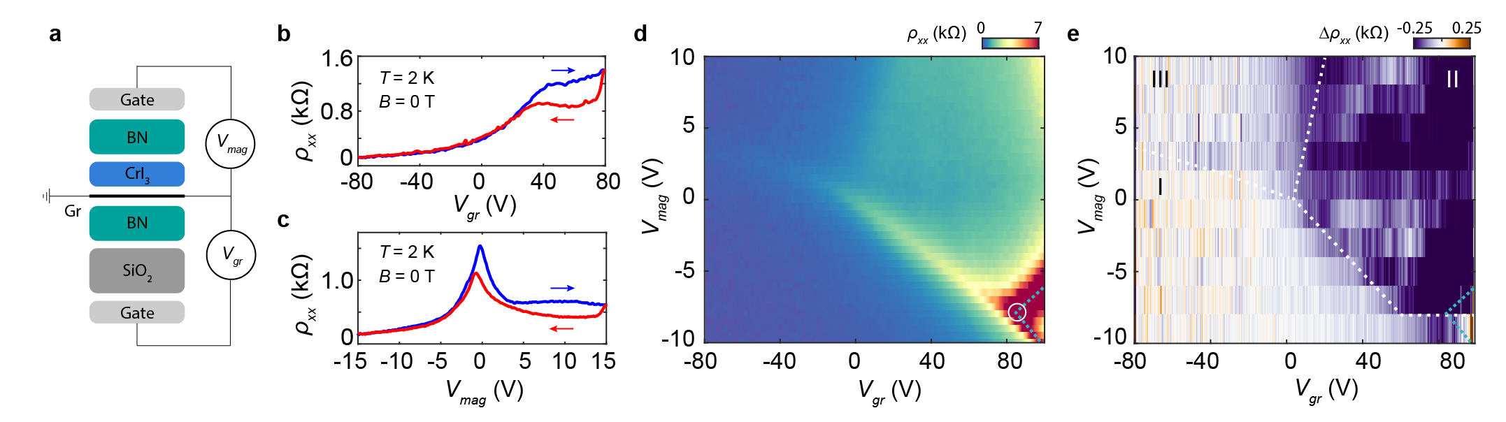
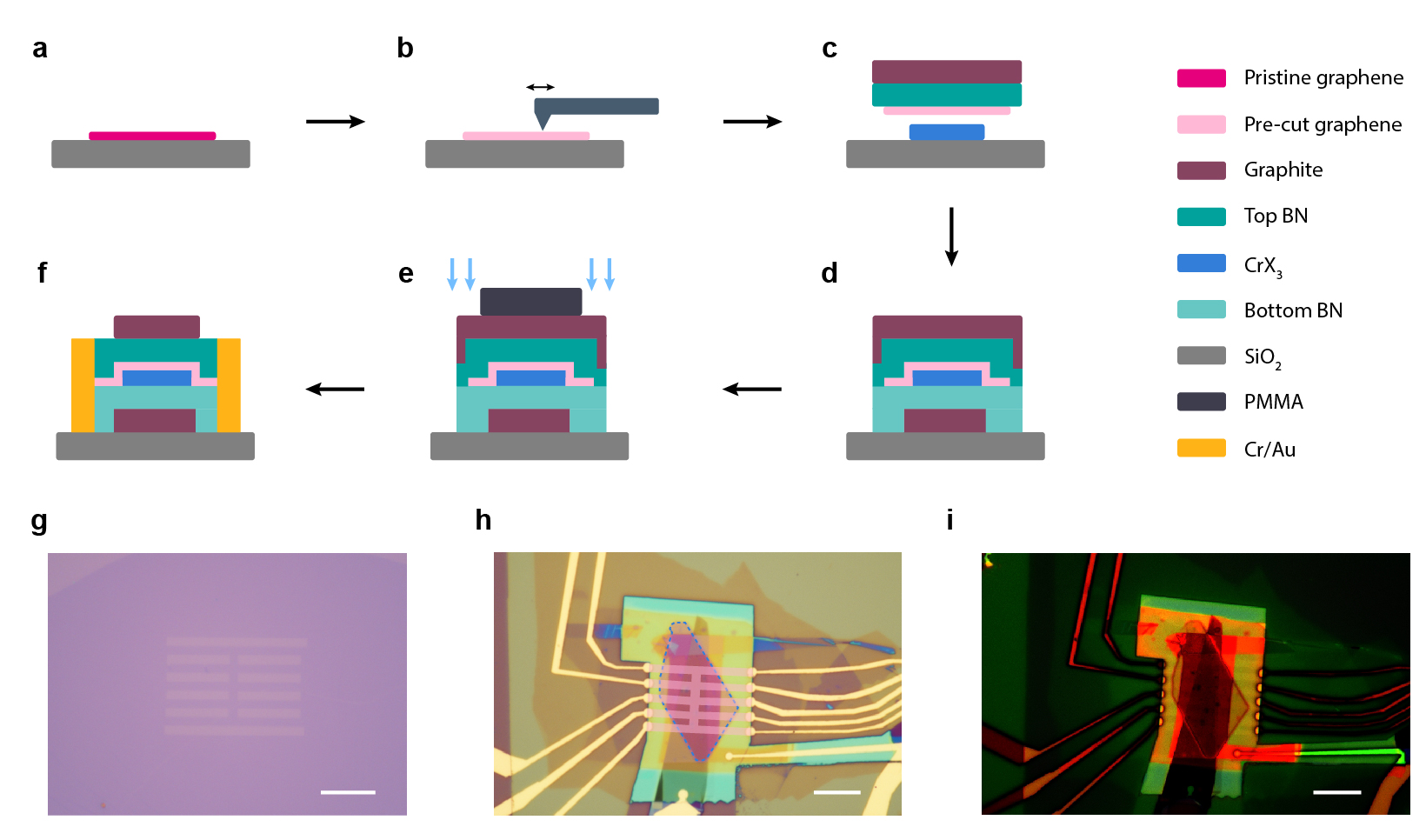
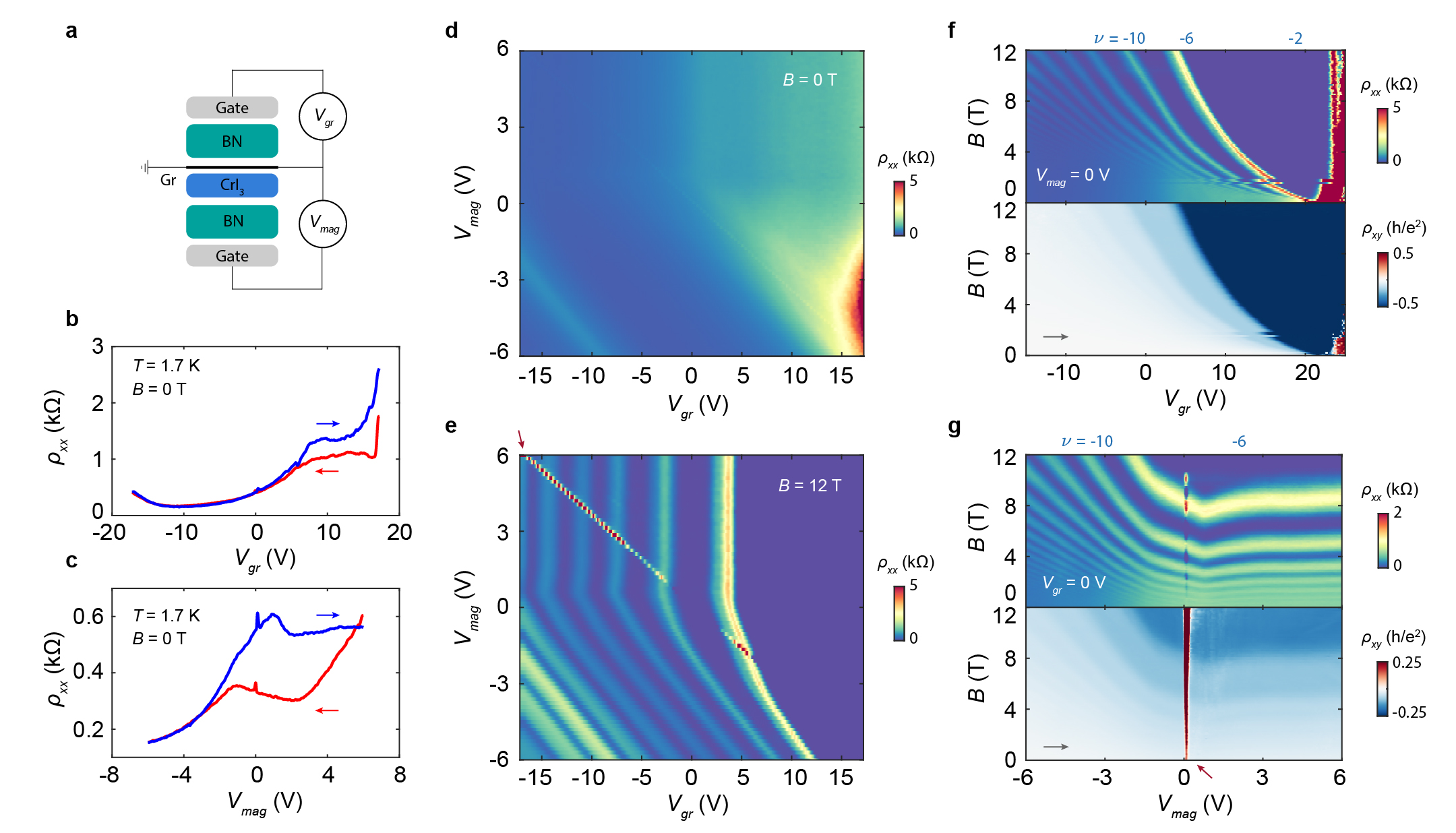
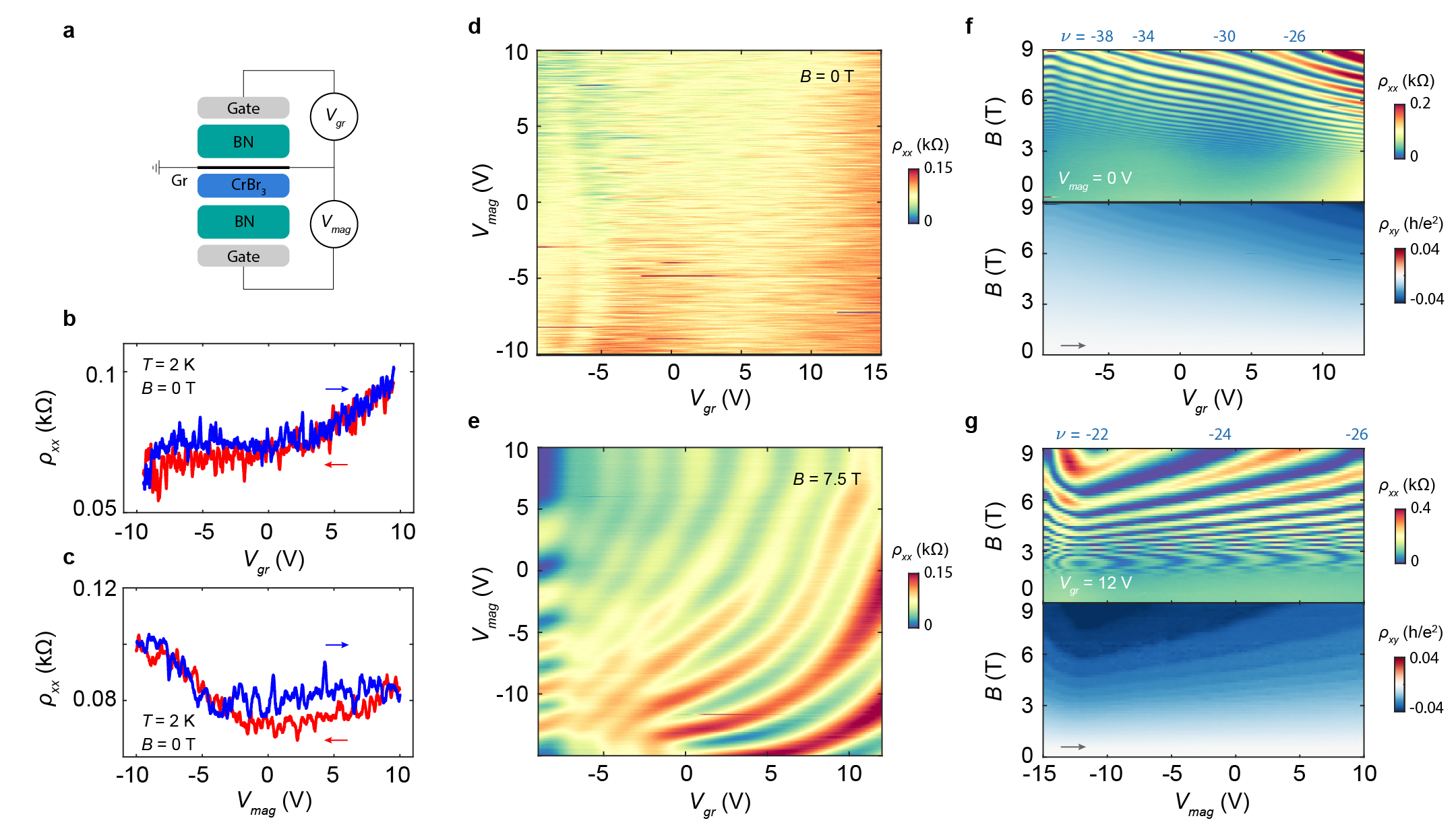
Here, we report low-temperature transport measurements of graphene on thin substrates of CrI3, CrBr3, and CrCl3 (collectively referred to as CrX3). Figure 1a shows a schematic of the general device structure we fabricate. Interfaces of graphene and thin CrX3 are encapsulated with boron nitride (BN) and surrounded by top and bottom gates. The CrX3 crystals we use range from three to tens of layers in thickness, however, the majority of our results do not appear to depend meaningfully on this parameter. In order to avoid degradation of the CrX3 crystals during device fabrication, we first shape a flake of exfoliated graphene into a Hall bar geometry using a polymer-free anodic oxidation technique with an atomic force microscope tip Li2018AON , and then assemble the entire vdW heterostructure in an argon-filled glovebox (see Methods and Supplementary Information Figs. S1 and S2 for full details). We fabricate devices in which the graphene rests atop CrX3, and visa versa, and see the same behavior in both cases. For clarity, we henceforth refer to the bias on the gate facing the graphene (CrX3) as ().
We focus our attention primarily on graphene/CrI3 heterostructures, from which we can additionally understand the salient properties of graphene/CrBr3 and CrCl3 (see Methods and Supplementary Figs. S8-S11). CrI3 has the lowest electron affinity of the three chromium trihalides, and as a result the modulation doping of the graphene is the smallest. Figure 1b (c) shows the resistivity of a graphene on trilayer CrI3 device (Device A) measured as () is swept back and forth with the other gate grounded at a temperature of K. We see a number of features that are uncharacteristic of pristine graphene encapsulated only with BN. First, the transport differs notably depending on which of the two gates is swept. Second, the transport is hysteretic, with the hysteresis most pronounced at positive values of either gate voltage. Although there are kinks or peaks in the resistivity suggestive of a Dirac point, measurements of the corresponding Hall resistance reveal that the graphene is hole-doped over most of the accessible gate voltage range (see Supplementary Information Fig. S3), indicating that these resistive peaks arise from a different mechanism.
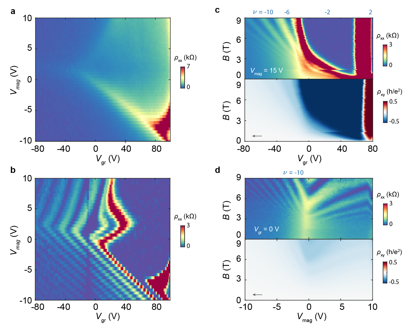
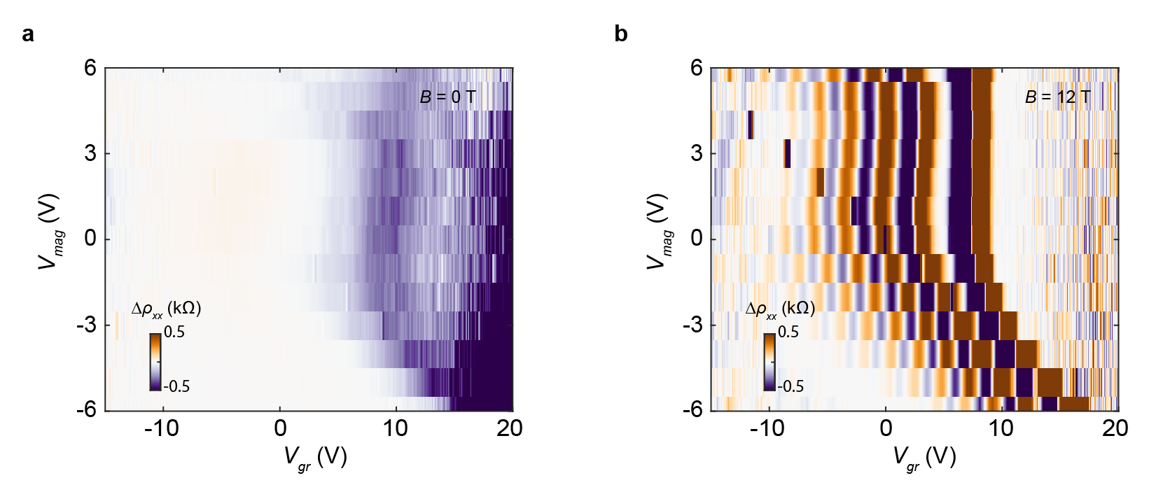
Figure 1d shows a map of the device resistivity acquired by sweeping both of the gates. The blue dashed curve traces the position of the Dirac point as determined by Hall effect measurements (Supplementary Information Fig. S3). The Dirac point evolves with the two gate voltages as anticipated from simple electrostatics in the bottom rightmost portion of the map. However, its trajectory abruptly reverses as the bias on is further reduced towards zero (white circle in Fig. 1d). The bent trajectory of the Dirac point indicates a nonlinear and nonmonotonic relationship between the gate voltage and graphene charge carrier density, in stark contrast with the behavior of conventional monolayer graphene devices in which the gate capacitance is fixed. We see other transport features atypical of graphene, including an anomalous resistive peak that moves roughly diagonally across the map, as well as an abrupt resistive step separating the top left and right halves of the map. There is also a sharp resistivity increase in the top rightmost corner of the map that indicates the reappearance of the Dirac point. Further, these features are directly associated with the hysteretic graphene transport. Figure 1e shows a measurement of acquired by taking the difference between measured as is slowly swept back and forth (see Supplementary Information Fig. S4 for the reverse measurements). As a guide to the eye, the white dashed curve denotes the positions of the anomalous resistive peaks we observe in Fig. 1d, and separates the map into Regions I, II, and III. The hysteresis is most prominent in Region II of the map, approximately bounded by the anomalous resistive peaks and plateaus.
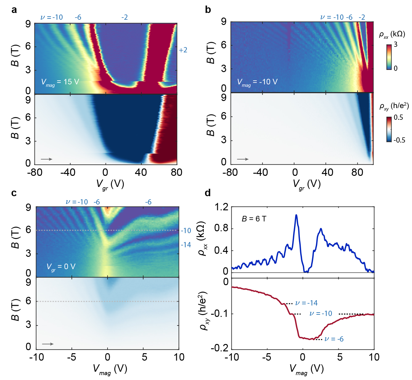
Transport measurements in a magnetic field, , help to reveal the origin of these unusual features. Figures 2a-b show Landau fan diagrams of the longitudinal, (top), and Hall, (bottom), resistivities acquired by sweeping from negative to positive bias with fixed values of V and V, respectively. The latter is consistent with typical hole-doped graphene: the Dirac point appears at large positive and is associated with a sign change in upon doping, and there is a series of integer quantum Hall (IQH) states that disperse linearly away from the Dirac point. These correspond to filling factors of , consistent with the usual sequence of states arising from spin- and valley-degenerate monolayer graphene Landau levels. In contrast, at V we see a number of anomalous features in the Landau fan, including the Dirac point drifting with magnetic field, an abrupt resistivity jump at T, extremely wide IQH plateaus, and IQH states at higher filling factors with slightly widened plateaus that move nonlinearly.
Landau fans acquired by sweeping at fixed exhibit even more striking peculiarities. Figure 2c shows a representative example, in which the IQH states disperse as expected for , but abruptly reverse direction for . The latter regime corresponds to an apparent negative compressibility of the system, in which applying more positive gate voltage results in filling additional hole-type Landau levels, rather than their anticipated depletion. Figure 2d shows a representative example of this phenomenon at T, in which the graphene exhibits two disconnected regimes of doping corresponding to the IQH state.
The IQH states in typical graphene devices fan out linearly from the Dirac point as the magnetic field is raised. Their trajectories are described by the Středa formula Streda1982 , , where is Planck’s constant, is the charge of the electron, and is the charge carrier density. Departure from this behavior provides further evidence of the nonlinear relationship between the gate voltage and the charge carrier density in the graphene originating from the charge transfer with the CrI3, consistent with the bent trajectory of the Dirac point observed in Fig. 1d. The wide IQH plateaus and their nonlinear trajectories in the fan diagram indicate that the charges induced by the gate do not accumulate in the graphene but rather fill the CrI3, since electrons become localized in the insulating CrI3 and do not contribute to transport. Related effects have been previously observed in graphene on SiC Lafont2015 ; Alexander-Webber2016 and CrOCl Wang2015gr-crocl . The coexistence of normal and atypical quantum Hall effects within our device suggests that the modulation doping can be controlled by gating, and under suitable conditions is even suppressed entirely.
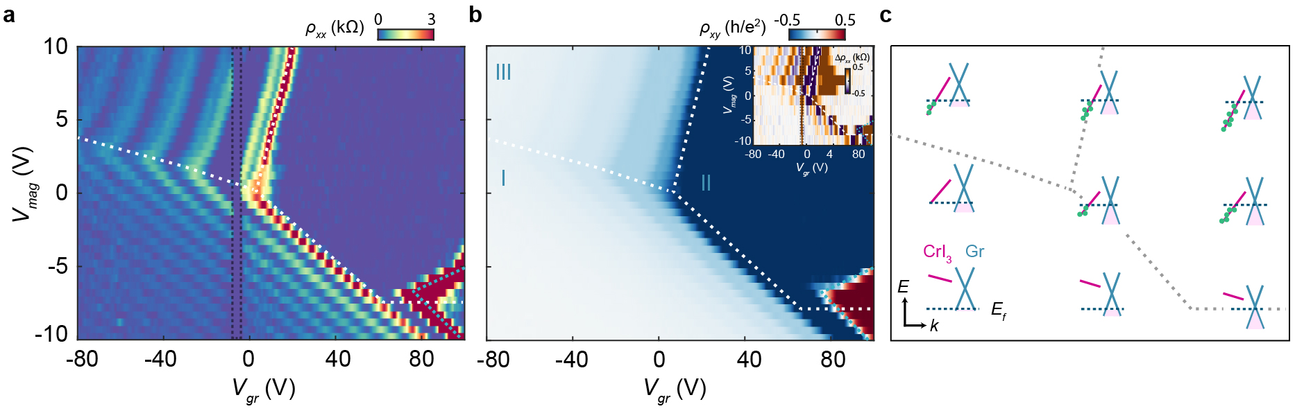
We characterize the full dependence of the charge transfer on gating and magnetic field by measuring and over the entire accessible range of both gate voltages at a fixed T (Fig. 3a-b). For the purposes of analyzing the behavior, we divide the map into three regions as marked by the white dotted lines (reproduced from Fig. 1e). Region I exhibits typical graphene magnetotransport, in which a sequence of hole-doped IQH states disperses diagonally. The negative slope of these features is consistent with the ratio of the geometrical capacitances of the top and bottom gates. This remains true for the insulating state in the bottom right corner of the map, across which the sign of the Hall effect flips. In contrast, Region II corresponds almost entirely to the IQH state. At the foot of Region II, we observe an abrupt reversal in the trajectory of the state similar to that of the Dirac point at (Fig. 1d). In Region III, the IQH states become nearly insensitive to and develop a positive slope. The inset of Fig. 3b shows hysteresis measurements, , acquired at T, analogous to the zero-field map shown in Fig. 1e. The hysteresis is primarily confined to Region III; however, we note that this measurement scheme is largely insensitive to hysteresis in Region II owing to the extended plateau. In combination with the zero-field measurements (Fig. 1e), we deduce that the device exhibits hysteresis in both Regions II and III. The hysteresis is therefore directly associated with regions of atypical graphene transport, and does not occur in Region I where the transport is conventional.
The above measurements can all be qualitatively understood by taking into account the gate- and field-dependent charge density in the CrI3. Figure 3c shows a series of cartoon diagrams that depict the electron states and their occupancies in the graphene (blue) and CrI3 (red) for different combinations of the top and bottom gate voltages. Filled states in graphene below the chemical potential (blue dashed line) are colored pink. The red line represents the lowest-energy electron states in the CrI3, and corresponds either to the bottom of the conduction band or a band of in-gap defect states; the latter is more likely because the charge mobility is very low. Electrons in the CrI3 are indicated by the green dots. We assume that the alignment between the graphene Dirac point and the lowest-energy electron band in the neighboring CrI3 layer is fixed by the combination of the graphene work function and CrI3 electron affinity. Biasing establishes an electric field across the few-layer CrI3, shifting the energy of the CrI3 states either up or down relative to the graphene.
Within Region I, the chemical potential lies beneath the lowest-energy electron states throughout the CrI3, and as a result they are all unoccupied. The CrI3 then simply behaves as a dielectric, and changing the bias on either gate capacitively dopes the graphene as usual. In Regions II and III, the bias is such that some electron states in the CrI3 are below the chemical potential, causing electrons to tunnel into them from the graphene. These electrons become almost entirely localized and contribute negligibly to the conductivity, but are mobile enough in the out-of-plane direction to screen the underlying gate. This results in a greatly altered sensitivity of the graphene doping to changes in . The hysteresis observed in these regions results from an inability of the electrons to reach a true equilibrium due to long timescales in the CrI3. As further evidence for this, we observe irreversible changes in the modulation-doping of the graphene in measurements performed days apart (see Supplementary Fig. S13), and in a graphene/CrCl3 device doped to a similar regime, the resistance exhibits telegraph noise on a timescale of tens of minutes when both gate voltages are held fixed (Supplementary Fig. S14).
The distinction between Regions II and III can be explained by the density of states in the graphene, which is small or vanishing in the former and much larger in the latter. These regions are separated by a resistivity plateau at zero field, and by a crossover at 9 T from the highly extended IQH plateau to a sequence of less extended IQH states with higher filling factors. In Region II, changes in are almost entirely screened. In this region, changing only weakly dopes the graphene because the low density of states means that adding electrons to the graphene causes its electrochemical potential to rise rapidly, leading to more electrons tunneling into the CrI3. In Region III, changing dopes the graphene more strongly because its density of states is larger. Meanwhile, changing does somewhat dope the graphene, but, strikingly, it does so in the wrong sense. In this case, the IQH states have positive slope indicative of an effectively negative differential capacitance. In other words, a more positive results in larger hole doping of the graphene, whereas naively it would be expected to instead reduce the hole doping. This effect is also responsible for the peculiar reversal of the trajectories of the IQH plateaus seen near in the Landau fans shown in Figs. 2c-d. Negative differential capacitance can result from negative compressibility in a strongly correlated conductor, such as has been reported for graphene on MoS2 Larentis2014 . It can also result from a large rearrangement of charge in the dielectric induced by a small change in applied electric field, such as occurs when a ferroelectric polarization flips. Rearrangement of the interacting electrons within the CrI3 therefore seems the most likely explanation for this phenomenon, and is consistent with the associated hysteresis, though it appears too complex to be usefully modeled at this point.
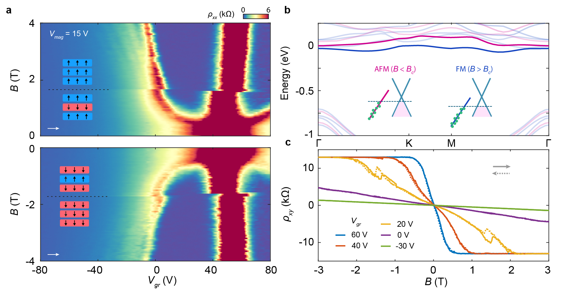
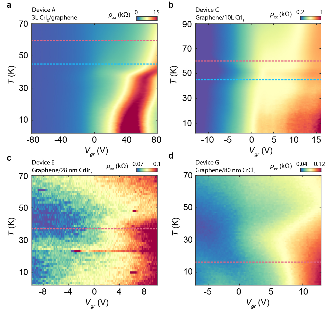
So far, we have not considered the role of the magnetic ordering of the CrI3, which exhibits out-of-plane intralayer ferromagnetism (FM) and antiferromagnet (AFM) interlayer ordering at low temperature. Figure 4a shows a low-field Landau fan diagram acquired for both positive and negative values of . As noted earlier, upon increasing the field there is an abrupt jump close to T at which all resistance features shift towards more positive , indicating a sudden transfer of electrons out of the graphene. To interpret this, we consider a simple model in which the CrI3 is a bilayer in order to investigate the origin of this effect, justified by the expectation that the graphene couples most strongly to the nearest few layers of the CrI3. Ab initio calculations show that the energy of the CrI3 conduction band depends on its interlayer magnetic ordering, shifting to lower energy as the material undergoes a transition from interlayer AFM to FM (Fig. 4b). This transition likely also reduces the energy levels of defect states, and results in additional electrons tunneling into the CrI3 (see band schematics in Fig. 4b). This abrupt jump is absent in Region I, where the states in the CrI3 remain too high to be occupied (e.g., see Fig. 2b). This effect demonstrates that the graphene resistivity is highly sensitive to the interlayer magnetic ordering of the CrI3. We find that the critical field becomes asymmetric with the sweeping direction of the magnetic field for thicker CrI3 substrates (Supplementary Information Fig. S17), indicating that the graphene is only sensitive to the magnetic ordering of the nearest few CrI3 layers.
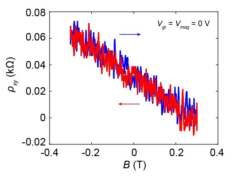
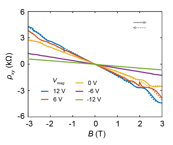
The anomalous Hall effect (AHE) is anticipated in graphene endowed with both a magnetic exchange field and Rasbha spin orbit coupling Qiao2010PRB ; Qiao2014PRL ; Zhang2015PRB ; Zhang2018PRB ; Hog2020PRB , owing to the formation of an inverted gap at the Dirac point and associated Berry curvature at the band edges. We search for the AHE by measuring as the magnetic field is swept back and forth at different values of (Figure 4c). We see hysteretic loops surrounding T owing to the AFM/FM transition in the CrI3, but do not observe hysteresis at . For measurements acquired nearby the Dirac point, we observe nonlinear surrounding reminiscent of a weak AHE. However, we also notice that the Dirac point drifts with magnetic field in the Landau fans shown in Fig. 2a and Fig. 4a. Although we do not understand the origin of this effect, and further find that it is highly sample dependent (e.g., see Supplementary Fig. S5f), its presence here implies that the charge transfer between the graphene and CrI3 changes continuously with the magnetic field. As a result, the charge carrier density in graphene also changes with at fixed gate voltage, potentially driving a nonlinearity in the observed Hall effect that is completely unrelated to the usual AHE mechanism.
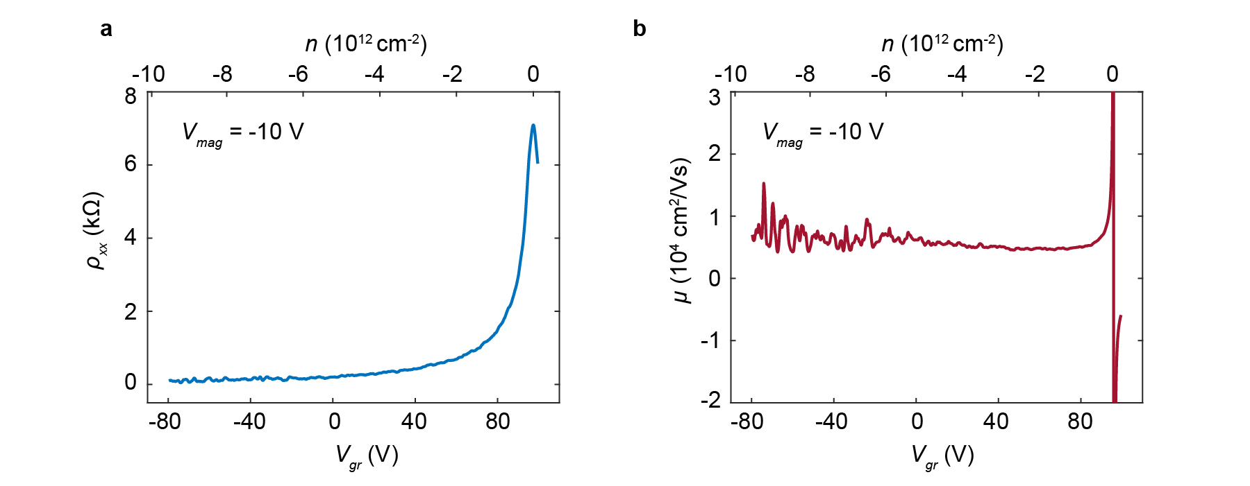
Careful analysis of the Landau fans can provide further insights into the strength of the magnetic proximity coupling in graphene. As detailed earlier, we observe a four-fold degeneracy in nearly all of the IQH states in our sample (with only weak signatures of symmetry-breaking at high ), indicating preserved spin and valley degeneracy. The absence of symmetry-broken IQH states is expected given the modest graphene mobility of cm2/Vs (see Supplementary Information Fig. S18), presumably resulting from scattering due to defects in the CrI3 substrate. However, the absence of detectable Landau-level splitting also sets an upper bound on the magnitude of the magnetic exchange coupling, which is expected to act as a Zeeman term that lifts the spin degeneracy at zero field. The magnetic exchange coupling must therefore be less than the smallest resolvable Landau level gap in our measurements. We estimate this to be 25 meV from the fact that the state fully develops at T (Fig. 4c), following the expectation that the corresponding cyclotron gap is , where m/s is the presumed Fermi velocity of graphene and is Planck’s reduced constant. This is in tension with theoretical predictions of magnetic exchange couplings ranging from tens of meV to as large as 120 meV in graphene on CrI3 Holmes2020 ; Farooq2019 ; Zhang2018PRBCrI3 . Furthermore, unambiguous evidence for a proximity exchange field has been observed in optical spectroscopy measurements of monolayer WSe2 on a CrI3 substrate Zhong2017SciAdv ; Zhong2020NatNano . The apparent unexpectedly small exchange coupling for graphene on CrI3 may be intrinsic, but it may also be degraded by disorder in the CrI3 for reasons that are not clear at present. Progress towards a high-temperature quantum anomalous Hall effect in proximitized graphene will likely require a reduction of the defect concentration in the CrI3 crystal, or the discovery of more favorable magnetic insulator substrates.
Methods
Device fabrication. Samples are assembled using a dry-transfer technique with a polycarbonate (PC)/polydimethyl siloxane (PDMS) stamp Wang2013 . The CrX3 must remain in an inert environment during the entire vdW assembly process to avoid crystal degradation. In order to achieve this, we first shape a flake of monolayer graphene into a Hall bar geometry using a polymer-free anodic oxidation lithography technique with an atomic force microscope tip Li2018AON . The vdW heterostructure consists of a graphene/CrX3 interface encapsulated between flakes of boron nitride. Additional graphite flakes enclad some samples to act as gates. The sample is deposited onto a Si/SiO2 wafer after assembly by melting the PC film at 180∘C. The entire vdW heterostructure assembly is performed inside a glovebox filled with argon. It is then removed from the glovebox, and the PC film is dissolved in chloroform. The CrX3 crystals are protected from degradation as long as they remain fully encapsulated by BN flakes. We use standard electron beam lithography, CHF3/O2 plasma etching, and metal deposition techniques (Cr/Au) in order to electrically contact the graphene Hall bar in regions far from the CrX3 flake. Supplementary Fig. S2 illustrates the fabrication procedure.
Transport measurements. Transport measurements were performed either in a Cryomagnetics variable temperature insert or a Quantum Design DynaCool PPMS, and were conducted in a four-terminal geometry with a.c. current excitation of 10-100 nA using standard lock-in techniques at a frequency of 13.3 Hz. In some cases, a gate voltage was applied to the Si gate in order to dope the region of the graphene contacts overhanging the graphite back gate to a high charge carrier density and reduce the contact resistance. The graphene resistivity, , is calculated from the measured resistance, , as , where is the Hall bar width and is the distance between the centers of the voltage probes of the graphene Hall bar. Unless otherwise stated, all measurements were performed at a base temperature of K.
Reproducibility of the transport in graphene/CrI3. We have characterized two additional graphene/CrI3 devices with CrI3 thicknesses of 7 and 10 layers (Supplementary Information Figs. S5-S7), as well as an additional 3 layer device with a monolayer of WSe2 sandwiched between the graphene and CrI3 (Supplementary Information Figs. S15-S16). Transport in all devices closely resembles that described in the device presented in the main text.
Transport in graphene on CrBr3 and CrCl3. In graphene on CrBr3 and CrCl3, the transport properties over the entire accessible gate voltage range closely resemble those of Region III for graphene on CrI3 (see Supplementary Figs. S8-S11). We see negative differential capacitance upon tuning over the entire accessible gate range, as well as hysteretic graphene transport. The differences among the CrX3 substrates arise as a consequence of the larger electron affinities of the CrBr3 and CrCl3, resulting in larger modulation doping of the graphene that cannot be suppressed by gating (i.e., we are unable to access the equivalent of Region I).
Temperature-dependent transport features at the onset of magnetic ordering. Supplementary Information Fig. S12 shows temperature-dependent transport measurements of graphene on CrI3, CrBr3, and CrCl3 across the critical temperature for magnetic ordering of each material. The graphene resistivity clearly changes within a few kelvin of the anticipated magnetic ordering temperature (dashed lines) for the case of CrI3, providing further evidence for the magnetic proximity effect. Although we do not understand the detailed origin of these features, they likely arise from a modification of the charge transfer as the CrI3 magnetically orders owing to a small energy shift of the bands. Temperature-dependent resistivity changes are also observed for CrBr3 and CrCl3, however they arise over a much broader range of temperature than for CrI3, and their connection to the onset of magnetic ordering is less obvious.
Acknowledgments
This work was supported as part of Programmable Quantum Materials, an Energy Frontier Research Center funded by the U.S. Department of Energy (DOE), Office of Science, Basic Energy Sciences (BES), under award DE-SC0019443. M.Y., X.X., and J.-H.C. acknowledge support from the State of Washington funded Clean Energy Institute. This work made use of shared fabrication facilities provided by NSF MRSEC 1719797. The material synthesis at UW is partially supported by the Gordon and Betty Moore Foundation’s EPiQS Initiative, Grant GBMF6759 to J.-H.C. K.W. and T.T. acknowledge support from the Elemental Strategy Initiative conducted by the MEXT, Japan (Grant Number JPMXP0112101001) and JSPS KAKENHI (Grant Numbers 19H05790, 20H00354 and 21H05233). M.M.’s crystal synthesis effort at ORNL was supported by the US Department of Energy, Office of Science, Basic Energy Sciences, Materials Sciences and Engineering Division.
Author contributions
C.-C.T. and T.S. fabricated the devices, with assistance from J.S. C.-C.T. and T.S. performed the measurements. Q.J., Z.L., and J.-H.C. provided the bulk CrI3 and CrBr3 crystals. M.M. provided the bulk CrCl3 crystals. K.W. and T.T. provided the bulk BN crystals. C.W. and D.X. calculated the CrI3 band structure. C.-C.T. and T.S. analyzed the data under the supervision of D.H.C., X.X. and M.Y.
Data Availability
Source data are available for this paper. All other data that support the plots within this paper and other findings of this study are available from the corresponding author upon reasonable request.
Competing interests
The authors declare no competing interests.
Additional Information
Correspondence and requests for materials should be addressed to M.Y.
Supplementary Information
Supplementary Sections S1-S10 and Figs. S1-S18.
References
- (1) Geim, A. K. & Grigorieva, I. V. Van der waals heterostructures. Nature 499, 419–425 (2013).
- (2) Wang, Z., Tang, C., Sachs, R., Barlas, Y. & Shi, J. Proximity-induced ferromagnetism in graphene revealed by the anomalous Hall effect. Physical Review Letters 114, 016603 (2015).
- (3) Wei, P. et al. Strong interfacial exchange field in the graphene/EuS heterostructure. Nature Materials 15, 711–716 (2016).
- (4) Leutenantsmeyer, J. C., Kaverzin, A. A., Wojtaszek, M. & van Wees, B. J. Proximity induced room temperature ferromagnetism in graphene probed with spin currents. 2D Materials 4, 014001 (2016).
- (5) Xu, J. et al. Spin inversion in graphene spin valves by gate-tunable magnetic proximity effect at one-dimensional contacts. Nature Communications 9, 2869 (2018).
- (6) Tang, C. et al. Approaching quantum anomalous Hall effect in proximity-coupled YIG/graphene/h-BN sandwich structure. APL Materials 6, 026401 (2018).
- (7) Karpiak, B. et al. Magnetic proximity in a van der Waals heterostructure of magnetic insulator and graphene. 2D Materials 7, 015026 (2019).
- (8) Tang, C., Zhang, Z., Lai, S., Tan, Q. & Gao, W.-B. Magnetic proximity effect in graphene/CrBr3 van der Waals heterostructures. Advanced Materials 32, 1908498 (2020).
- (9) Wu, Y. et al. Large exchange splitting in monolayer graphene magnetized by an antiferromagnet. Nature Electronics 3, 604–611 (2020).
- (10) Ghiasi, T. S. et al. Electrical and thermal generation of spin currents by magnetic bilayer graphene. Nature Nanotechnology 16, 788–794 (2021).
- (11) Wu, Y. et al. Magnetic exchange field modulation of quantum hall ferromagnetism in 2d van der waals crcl3/graphene heterostructures. ACS Applied Materials and Interfaces 13, 10656–10663 (2021).
- (12) Chau, T. K., Hong, S. J., Kang, H. & Suh, D. Two-dimensional ferromagnetism detected by proximity-coupled quantum Hall effect of graphene. npj Quantum Materials 7, 27 (2022).
- (13) Qiao, Z. et al. Quantum anomalous Hall effect in graphene from Rashba and exchange effects. Physical Review B 82, 161414 (2010).
- (14) Qiao, Z. et al. Quantum anomalous Hall effect in graphene proximity coupled to an antiferromagnetic insulator. Physical Review Letters 112, 116404 (2014).
- (15) Zhang, J., Zhao, B., Yao, Y. & Yang, Z. Robust quantum anomalous Hall effect in graphene-based van der Waals heterostructures. Physical Review B 92, 165418 (2015).
- (16) Zhang, J. et al. Strong magnetization and Chern insulators in compressed graphene/CrI3 van der Waals heterostructures. Physical Review B 97, 085401 (2018).
- (17) Hög, P. et al. Quantum anomalous Hall effects in graphene from proximity-induced uniform and staggered spin-orbit and exchange coupling. Physical Review B 124, 136403 (2020).
- (18) Avsar, A. et al. Spin–orbit proximity effect in graphene. Nature Communications 5, 4875 (2014).
- (19) Wang, Z. et al. Strong interface-induced spin–orbit interaction in graphene on WS2. Nature Communications 6, 8339 (2015).
- (20) Wang, Z. et al. Origin and magnitude of ‘designer’ spin-orbit interaction in graphene on semiconducting transition metal dichalcogenides. Physical Review X 6, 041020 (2016).
- (21) Yang, B. et al. Tunable spin–orbit coupling and symmetry-protected edge states in graphene/ws2. 2D Materials 3, 031012 (2016).
- (22) Island, J. O. et al. Spin-–orbit-driven band inversion in bilayer graphene by the van der waals proximity effect. Nature 571, 85–89 (2019).
- (23) Huang, B. et al. Layer-dependent ferromagnetism in a van der Waals crystal down to the monolayer limit. Nature 546, 270–273 (2017).
- (24) Zhang, Z. et al. Direct photoluminescence probing of ferromagnetism in monolayer two-dimensional CrBr3. Nano Letters 19, 3138–3142 (2019).
- (25) Cai, X. et al. Atomically thin CrCl3: an in-plane layered antiferromagnetic insulator. Nano Letters 19, 3993–3998 (2019).
- (26) Li, H. et al. Electrode-free anodic oxidation nanolithography of low-dimensional materials. Nano Letters 18, 8011–8015 (2018).
- (27) Streda, P. Quantised hall effect in a two-dimensional periodic potential. Journal of Physics C: Solid State Physics 15, L1299 (1982).
- (28) Lafont, F. et al. Quantum hall resistance standards from graphene grown by chemical vapour deposition on silicon carbide. Nature Communications 6, 6806 (2015).
- (29) Alexander-Webber, J. A. et al. Giant quantum Hall plateaus generated by charge transfer in epitaxial graphene. Scientific Reports 6, 30296 (2016).
- (30) Wang, Y. et al. Flavoured quantum hall phase in graphene/CrOCl heterostructures. arXiv:2110.02899 (2021).
- (31) Larentis, S. et al. Band offset and negative compressibility in graphene-mos2 heterostructures. Nano Letters 14, 2039–2045 (2014).
- (32) Holmes, A. M. et al. Exchange splitting and exchange-induced nonreciprocal photonic behavior of graphene in CrI3-graphene van der Waals heterostructures. Physical Review B 102, 075435 (2020).
- (33) Farooq, M. U. & Hong, J. Switchable valley splitting by external electric field effect in graphene/CrI3 heterostructures. npj 2D Materials and Applications 3, 33 (2019).
- (34) Zhang, J. et al. Strong magnetization and Chern insulators in compressed graphene/CrI3 van der Waals heterostructures. Physical Review B 97, 085401 (2018).
- (35) Zhong, K. L., D. Seyler et al. Van der Waals engineering of ferromagnetic semiconductor heterostructures for spin and valleytronics. Science Advances 3, e1603113 (2017).
- (36) Zhong, D. et al. Layer-resolved magnetic proximity effect in van der Waals heterostructures. Nature Nanotechnology 15, 187–191 (2020).
- (37) Wang, L. et al. One-dimensional electrical contact to a two-dimensional material. Science 342, 614–617 (2013).
- (38) Behera, S. K., Bora, M., Chowdhury, S. S. P. & Deb, P. Proximity effects in graphene and ferromagnetic CrBr3 van der Waals heterostructures. Physical Chemistry Chemical Physics 21, 25788–25796 (2019).
- (39) McGuire, M. A. et al. Magnetic behavior and spin-lattice coupling in cleavable van der waals layered crcl3 crystals. Physical Review Materials 1, 014001 (2017).
- (40) Huang, B. et al. Emergent phenomena and proximity effects in two-dimensional magnets and heterostructures. Nature Materials 19, 1276–1289 (2020).
- (41) Zhou, B. et al. Evidence for charge transfer and proximate magnetism in graphene–−RuCl3 heterostructures. Physical Review B 100, 165426 (2019).
- (42) Song, T. et al. Giant tunneling magnetoresistancein spin-filter van der Waals heterostructures. Science 360, 1214–1218 (2018).
- (43) Song, T. et al. Voltage control of a van der Waals spin-filter magnetic tunnel junction. Nano Letters 19, 915–920 (2019).
- (44) Kim, H. H. et al. One million percent tunnel magnetoresistance in a magnetic van der Waals heterostructure. Nano Letters 18, 4885–4890 (2018).
- (45) Wang, Z. et al. Very large tunneling magnetoresistance in layered magnetic semiconductor CrI3. Nature Communications 9, 2516 (2018).
- (46) Kim, H. H. et al. Evolution of interlayer and intralayer magnetism in three atomically thin chromium trihalides. The Proceedings of the National Academy of Sciences 116, 11131–11136 (2019).
Supplementary Information
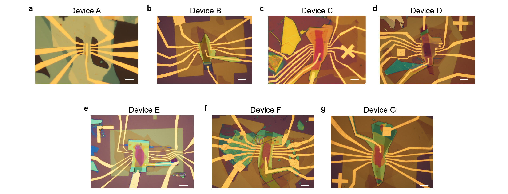
S1. Summary of the graphene/CrX3 devices
We study six devices of graphene on various CrX3 substrates, and one device with a monolayer WSe2 spacer. Table S1 summarizes the details of these devices. Data in the main text is acquired from Device A. Figure S1 shows optical micrographs of all seven devices. Device A has a silicon back gate and gold top gate. All other devices have graphite top and bottom gates. Figure S2 illustrates the fabrication procedure for our devices (see Methods for additional discussion of the device fabrication).
| Device | Material | CrX3 Thickness |
|---|---|---|
| A | CrI3 | 3 layers |
| B | CrI3 | 7 layers |
| C | CrI3 | 10 layers |
| D | WSe2/CrI3 | 1/3 layers |
| E | CrBr3 | 28 nm |
| F | CrCl3 | 40 nm |
| G | CrCl3 | 80 nm |
S2. Determination of the carrier type and Dirac point trajectory in Device A
S3. Transport in Device A acquired in the reverse gate sweeping condition
All transport data for Device A in the main text is acquired by sweeping the fast-axis gate from negative to positive values. Figure S4 shows comparable measurements acquired by instead sweeping the fast-axis gate from positive to negative. Transport differs primarily in Regions II and III, as evidenced by the hysteresis maps in Figs. 1e and 3b (inset) of the main text.
S4. Transport characterization of additional graphene/CrI3 devices
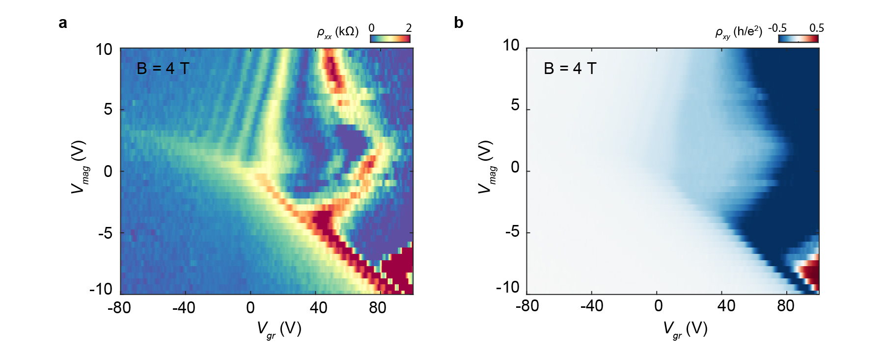
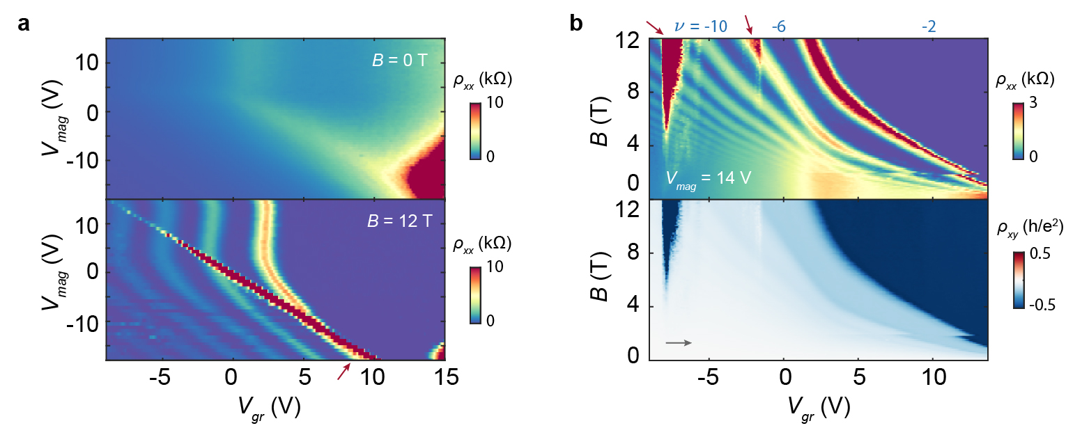
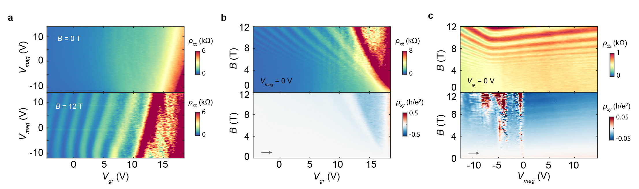
We have studied two graphene/CrI3 devices (Devices B and C) in addition to the one reported in the main text (Device A). These two devices have thicker CrI3 substrates of 7 and 10 layers, respectively. Figure S5a shows a schematic of Device C, which has graphite top and bottom gates. Figures S5b-c show the device resistivity acquired by sweeping one gate back and forth with the other grounded, and Fig. S5d shows the resistivity map acquired by sweeping both gates, analogous to the measurements of Figs. 1b-d of the main text for Device A. The basic transport phenomenology is nearly identical between the two devices, including the gate-tunable modulation doping, the bent trajectory of the Dirac point, anomalous resistive peaks and plateaus in the hole-doped regime, and hysteresis confined only to certain portions of the phase diagram. We note that this device appears to be aligned with the encapsulating boron nitride and manifests a weak secondary Dirac point at large hole doping (diagonal feature in the bottom left of Fig. S5d), however, this does not appear to have a meaningful impact on the overall transport properties arising from the graphene/CrI3 interface. Figure S5e shows a similar resistivity map at T, and Figs. S5f-g show Landau fan diagrams of the longitudinal (top) and Hall (bottom) resistivities acquired by sweeping and , respectively, with the other gate held at ground. Again, we see that this device reproduces the salient high-field features of Device A reported in the main text, including a highly extended plateau, nonlinear trajectories of the IQH states, signatures of negative compressibility when tuning in the equivalent of Region III, and an abrupt jump in the modulation doping around the magnetic field at which the CrI3 becomes a layer ferromagnet.
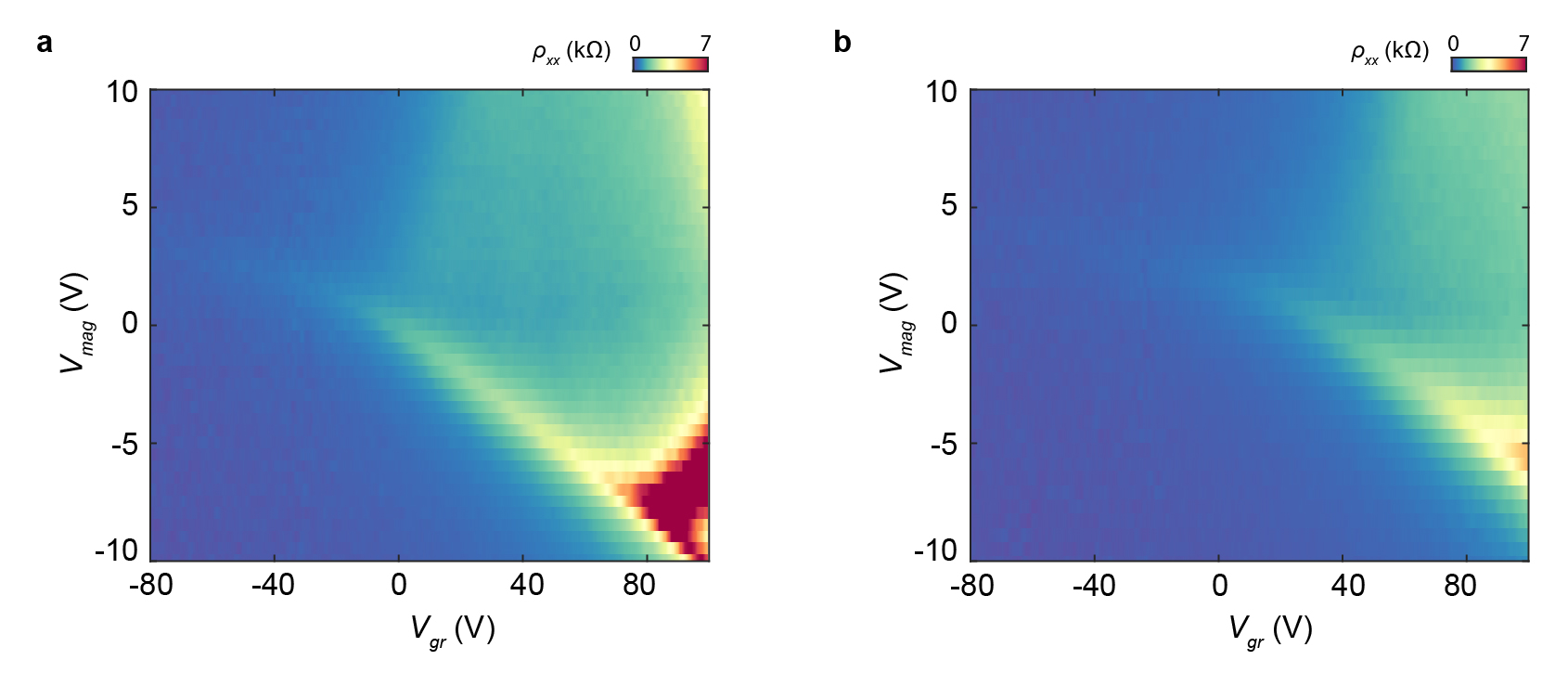
Figures S6a-b show the hysteresis maps of this device acquired at and 12 T, respectively. As in Device A, the combination of these measurements reveals hysteretic behavior everywhere except the bottom left portion of the map (Region I). Device B also behaves quite similarly overall (Fig. S7), indicating excellent reproducibility of the transport properties of graphene/CrI3 heterostructures.
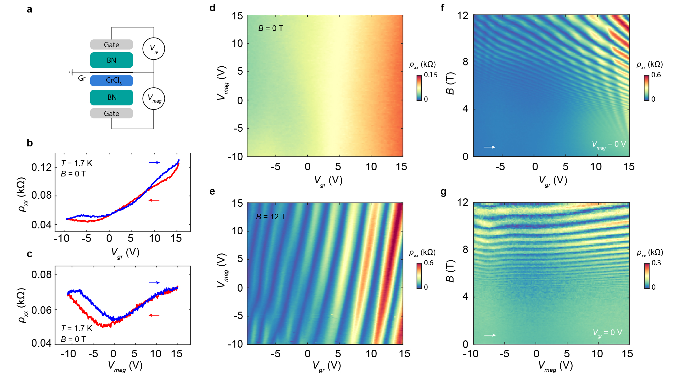
S5. Transport characterization of graphene on CrBr3 and CrCl3
We have performed transport characterization similar to that described in the main text for graphene/CrBr3 and graphene/CrCl3 heterostructures. CrBr3 is both an intra- and inter-layer ferromagnet at low temperature. We construct a dual graphite-gated device with a graphene/CrBr3 interface (Fig. S8a) and measure the graphene resistivity as a function of each gate (Figs. S8b-c). Upon sweeping both gates, we find that the graphene resistivity is very low over the entire accessible range of doping (Fig. S8d), with much smaller gate-induced changes in resistivity than in graphene/CrI3. In a similar measurement at T, we see IQH states that exhibit highly unusual trajectories as a function of gating. These states move nonlinearly with gate voltage, and disperse in the opposite direction than anticipated upon gating with indicative of an apparent negative compressibility.
These observations are corroborated by measurements of the Landau fan diagrams. In the fan acquired by tuning at fixed (Fig. S8f), we observe magnetotransport that is mostly consistent with typical highly-doped graphene. The four-fold degenerate IQH states disperse nearly linearly with , projecting to a very positive indicating large modulation hole doping. Corresponding measurements of further corroborate the large filling factors of the IQH states and their hole-type doping. In contrast, the Landau fan acquired by tuning at fixed V is highly atypical, with IQH states dispersing away from the apparent Dirac point over the majority of the accessible gate range (Fig. S8g). The upturn of these states at very negative is a consequence of hysteresis in the system. These oppositely dispersing IQH states indicate the negative differential capacitance of the system upon tuning over the entire accessible gate range of the device. These observations are phenomenologically consistent with Region III of the graphene/CrI3 phase diagram, and indicate that the electron affinity of CrBr3 is larger than CrI3. In this case, the lowest electron band of CrBr3 resides below the Dirac point of graphene, resulting in modulation doping that cannot be suppressed with gating.
We do not find any signs of a magnetic exchange field in the graphene, very similar to the case of graphene/CrI3. We observe an ordinary (linear) Hall effect over the entire accessible gate range (see Fig. S9 for a representative example), although this is expected even in the case of a sizable magnetic exchange field since the Berry curvature is likely concentrated close to the Dirac point. However, we do not observe any signatures of degeneracy lifting in the main-sequence IQH states. We follow a similar analysis of the quantum Hall gap as described in the main text to estimate the approximate upper bound strength of the magnetic exchange field as 15 meV, which is similar to that of graphene/CrI3. In contrast, calculations suggest exchange couplings of 70 meV in graphene on CrBr3 Behera2019CrBr3 . As in graphene/CrI3, this rough upper bound estimate is much less than the theoretical expectation, and the reason for the discrepancy is not presently clear.
CrCl3 is an intralayer ferromagnet and interlayer antiferromagnet. Spins in CrCl3 are aligned in the 2D plane, rather than perpendicular as in CrI3 and CrBr3, although bulk CrCl3 requires an out-of-plane field of only T to fully polarize its spins out of the 2D plane McGuire2017 . In spite of the different magnetic structure, we find that transport in graphene/CrCl3 heterostructures is qualitatively consistent with CrBr3. Figure S10a shows the device structure for a sample of graphene on an 80 nm thick CrCl3, and Figs. S10b-g show transport measurements analogous to those presented for the graphene/CrBr3 device in Fig. S8. Although the exact details differ, the basic properties look very similar. We find that the apparent modulation doping is slightly less in a second device with a 40 nm CrCl3 (Fig. S11, as we are just barely able to access the Dirac point by gating. At present, it is not clear what controls the precise amount of modulation doping in graphene/CrCl3 devices. Despite this ambiguity, the majority of the accessible gate range in both devices phenomenologically corresponds to the behavior of Region III described in the main text.
S6. Temperature-dependent transport of graphene/CrX3
Figure S12 shows the resistivity of graphene on CrI3, CrBr3, and CrCl3 measured as a function of temperature and at fixed . The overall resistivity drifts with temperature in ways that we do not fully understand, however, in the case of CrI3 we see clear resistivity jumps within a few kelvin of the anticipated magnetic ordering temperature (denoted by the blue dashed line for the case of monolayer CrI3 and the red dashed line for the case of bulk CrI3 Huang2020review ). This indicates that the onset of magnetism in the CrI3 impacts the graphene transport, likely by changing the magnitude of the modulation doping as the band edge shifts. Similar effects have been observed previously in graphene/RuCl3 heterostructures Zhou2019RuCl3 . The resistivity drifts over a much wider range of temperature for CrBr3 and CrCl3 substrates, and the potential connection of these features with magnetic ordering is less clear.
S7. Characterization of hysteresis timescales
We routinely observe hysteresis over long time scales in our graphene/CrX3 devices. Figures S13 and S14 illustrate this from two different perspectives. Figure S13 shows two identical dual gate maps at acquired three days apart in Device A (but within the same cooldown). All of the features rigidly shift towards more positive values of . In particular, the Dirac point drifts almost entirely outside of the accessible gate range. The precise origin of this long-term drifting feature is not known, but must be related to slow charging effects of the CrI3.
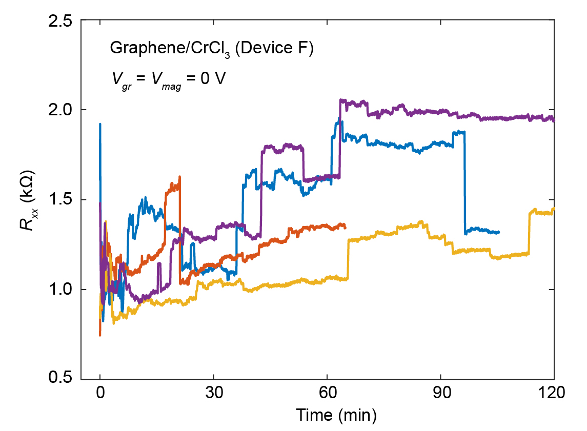
Figure S14 shows in a graphene/CrCl3 device (Device F) measured as a function of time at T. The measurement is initialized by quickly sweeping from 10 V to 0 V with , and then waiting at V while recording the device resistivity. Four consecutive measurements are performed in order to understand the reproducibility of the results, each shown in a different color. We see that the resistivity drifts upwards in all measurements over the span of at least two hours. We also observe large, abrupt jumps in the resistivity to both larger and smaller values at apparently random times. This telegraph noise indicates spontaneous mesoscopic rearrangement of the nearly-localized charges in the CrCl3. Together, these measurements indicate the inability of the electrons to reach equilibrium in the CrX3 substrates.
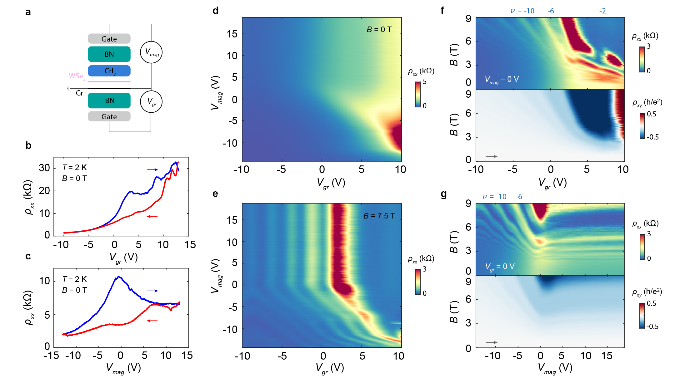
S8. Transport in a graphene/WSe2/CrI3 heterostructure
Interfacing graphene with WSe2 (and similar transition metal dichalcogenides) is known enhance the spin-orbit coupling of the graphene Avsar2014NatCom ; Wang2015NatCom ; Wang2016PRX ; Yang2016SOC ; Island2019 . We have additionally fabricated devices in which there is a monolayer of WSe2 in between the graphene and the CrI3. We find that even with the monolayer WSe2 spacer layer, there is similar modulation doping of the graphene due to charge transfer with the CrI3. Figure S15 summarizes our primary observations in this device. Overall, we find that transport in this structure closely resembles the graphene/CrI3 devices. We observe an ordinary Hall effect even very near the Dirac point (Fig. S16), indicating the absence of the AHE in this system.
S9. Sensing the surface magnetic ordering of bulk CrI3 with graphene
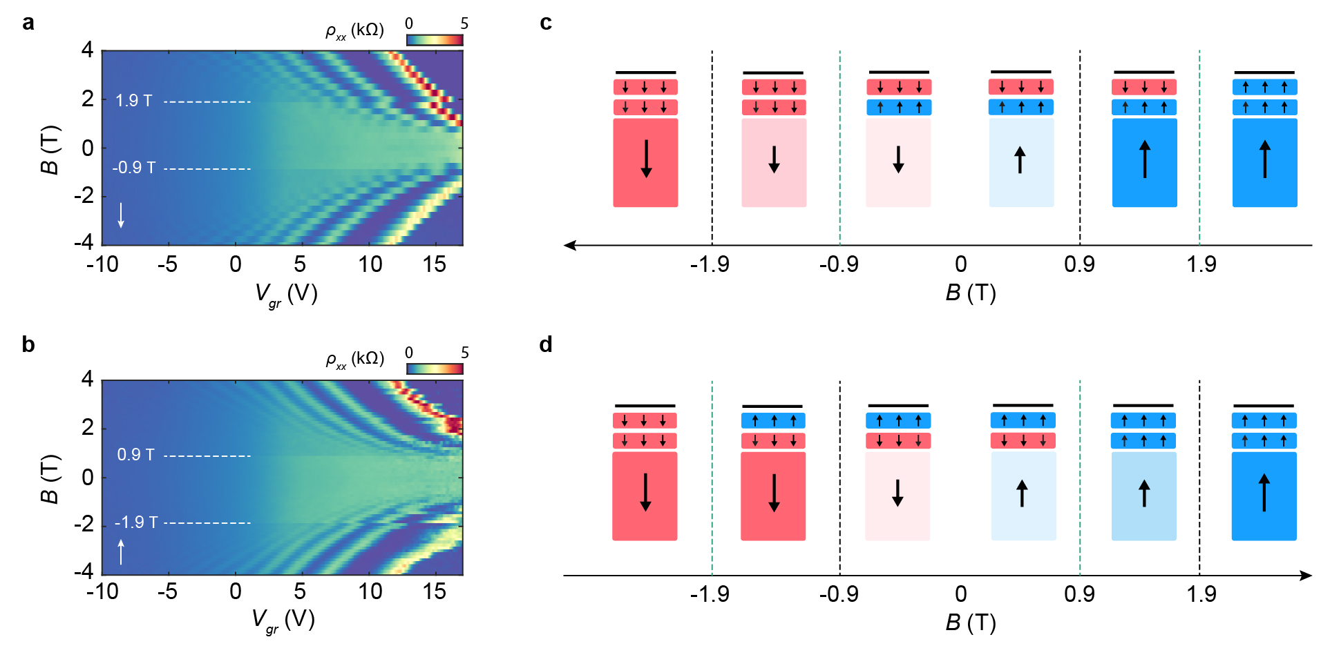
Figure S17a (b) shows a Landau fan diagram of a graphene on 10 layer CrI3 device (Device C) acquired by changing at fixed V, and with swept from positive to negative (negative to positive) values. We observe one abrupt jump in the modulation doping at all values of for each sign of , as indicated by the white dashed lines (other small jumps are also occasionally observed, but only occur over small ranges of and likely arise due to randomly moving charges in the CrI3). Unlike for the 3 layer CrI3 device in which these jumps occur at the same absolute value of , we find an asymmetry in the switching field in the 10 layer device. In particular, the first jump occurs when the field crosses T, and the second jump occurs when the opposite sign of the field exceeds T.
Magnetic switching at fields of 0.9 T and 1.9 T (in addition to at many smaller fields) is routinely observed in magnetic tunnel junction (MTJ) measurements of CrI3 up to ten layers Song2018SciCrI3MTJ ; Song2019NanolettCrI3MTJ ; Kim2018NanolettCrI3MTJ ; Wang2018NatComCrI3MTJ ; Kim2019PNASCrI3MTJ . These structures, consisting of graphite/few-layer CrI3/graphite, exhibit symmetric tunneling properties for both signs of the magnetic field. In contrast, our transport measurements are inherently asymmetric, since the graphene layer sits only on one side of the CrI3. Seeing jumps in the modulation doping at different fields depending on the field sweeping direction indicates that the graphene is sensitive only to the spin configuration of the nearest few CrI3 layers. The schematics in Figs. S17c-d illustrate one possible evolution of the interlayer spin arrangement as the magnetic field is swept. Starting from the interlayer ferromagnetic configuration at high field, our results are consistent with the spins in the CrI3 layer neighboring the graphene flipping first at T. In contrast, the spins in the second layer do not flip until the field reaches a value of 0.9 T with the opposite sign. The spins in the remaining bulk layers likely flip in a correlated fashion, however, the graphene transport is apparently not sensitive to these spin flips.
S10. Mobility of hole-type carriers in graphene on CrI3