Graphene-based quantum Hall interferometer with self-aligned side gates
Abstract
The vanishing band gap of graphene has long presented challenges for making high-quality quantum point contacts (QPCs) – the partially transparent p-n interfaces introduced by conventional split-gates tend to short the QPC. This complication has hindered the fabrication of graphene quantum Hall Fabry-Pérot interferometers, until recent advances have allowed split-gate QPCs to operate utilizing the highly resistive state. Here, we present a simple recipe to fabricate QPCs by etching a narrow trench in the graphene sheet to separate the conducting channel from self-aligned graphene side gates. We demonstrate operation of the individual QPCs in the quantum Hall regime, and further utilize these QPCs to create and study a quantum Hall interferometer.
keywords:
Graphene, Quantum Point Contacts, Quantum Hall Interferometer, Side-gatesQuantum Hall (QH) interferometers have long provided valuable information about the nature of the edge state and excitations in a variety of QH systems 1, 2. Key elements of these interferometers are the quantum point contacts (QPCs) – the gate-defined constrictions that backscatter the QH edge channels. In comparison to GaAs, QPCs are challenging to make in graphene because of its vanishing band gap. The development of graphene QPCs mostly focused on making split-gates on top of boron nitride 3, 4. Recently, such QPCs with state underneath the split-gates have been used to make Fabry-Pérot interferometers 5, 6. Ultra-clean QPCs operating in the fractional QH regime have also been demonstrated 7.
Although QPCs in GaAs systems are most commonly made in a top-gated geometry, there have also been a number of successful designs based on side-gated QPCs defined by etched trenches. The side-gated design offers some advantages, for example allowing one to induce spin-orbit interactions via asymmetric gating. Most recently, the side-gated QPCs have been fabricated in suspended mechanical nanostructures 8. On the flip side, fabricating clean QPCs is more challenging in the side-gated vs. top-gated geometry due to the roughness introduced by reactive ion etching. However, recently, it has been demonstrated that the cleanness of side-gated QPCs in graphene can be substantially improved using cryo-etching 9 or AFM lithography 10, 7. In terms of fabrication difficulty, top-gated QPCs are easier for GaAs but more challenging for graphene in comparison to the side-gated design. Furthermore, the top gates forming the QPC in graphene have a tendency to be leaky in the lateral direction due to the partially transparent PN junctions formed under them, which is particularly relevant at low magnetic fields 4, 11. At a high magnetic field, one of the major applications of QPCs is to explore the anyon statistics in fractional QH interferometers. The recently achieved ultra-clean top-gates QPCs revealed an important complication in this direction –- the edge reconstruction effects of fractional QH states are substantial due to the smooth electrostatic confinement in such structures 7. Almost at the same time, a STM investigation evidenced the absence of edge reconstruction for hard-wall confinement in graphene 12. Since the confinement potential of side-gated QPCs is much sharper, they may have great potential in exploring the transport of fractional QH edges with suppressed edge reconstruction.
Here, we explore side-gated graphene QPCs by etching self-aligned side-gates and constrictions in graphene/hBN stacks. Such side-gate controlled QPCs may present a simpler alternative to their top-gated counterparts 4, 5, 6, 7. The design follows earlier works on graphene nanostructures 13, 14, 15 and our recent work, which showed that self-aligned side gates could efficiently tune the QH filling factor near the edge of graphene 16. We further characterize the Fabry-Pérot interferometer defined by a pair of QPCs, and find it in the Coulomb interaction dominated regime 17. The charging effects are also manifested via phase jumps when localized charge states are filled either in the interferometer or nearby graphene gates. Following the equilibrium single-particle picture 18, we extract the edge state velocity of the spin-polarized edge state at from the energy scale measured via the bias dependence of the interference patterns. The temperature dependence of the interference visibility is found to be consistent with this energy scale.
1 Side-gate controlled QPCs
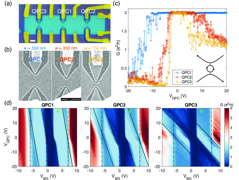
Our device consists of a monolayer graphene crystal encapsulated in hexagonal boron nitride 19. The stack is deposited on a SiO2/Si substrate, which serves as the back-gate (BG). We use conventional electron-beam lithography and reactive ion etching to fabricate three QPCs in the same graphene crystal (Fig. 1(a), see details in Methods). The constriction widths of the three QPCs are 550, 350 and 150 nm, respectively. Both the QPC constrictions and the side gates are formed in the same etching step, as shown in Fig. 1(b). Here, the QPC channels are horizontal, and the triangular-shaped graphene regions that are etched away from the channel are used as the side gates. Both the side gates and the main region of graphene are contacted via thermally evaporated Cr/Au. The gap between the channel and the side gate at their closest separation is 50 nm and grows wider as one moves further away from the QPC. This design is intended to reduce the undesired gating away from the QPCs.
To characterize the efficiency of the QPCs as a function of constriction width, we measure their two-probe differential conductance, (Methods). All data presented in this paper are taken at 100 mK unless noted otherwise. In Fig. 1 (c), we show the conductance of all three QPCs as a function of at a magnetic field of T and a back-gate voltage V (bulk filling factor ). When the bulk is n-doped, applying a negative side gate voltage gradually reduces to zero. This is due to the carrier depletion in the constriction, which causes a reduction of the transmission probability of the edge states. Applying a high positive side gate voltage can introduce additional Landau-levels inside the constrictions, which helps to equilibrate the chemical potential of the counter-propagating edge states 4. Further increasing results in a reduction of , which saturates at when the equilibration process is complete. At this point the constriction effectively serves as a floating contact, thereby doubling the QPC resistance.
As expected, the tuning efficiency of the side gates is higher for the narrower QPCs. Indeed, the extent of the plateau in Fig. 1(c) shrinks as the constriction becomes progressively narrower. While the resulting higher tunability of the QPC is an attractive feature, the degree of conductance quantization eventually degrades. Patches of reduced conductance are seen in the middle of the plateau of QPC3. Moreover, the counterpropagating channels rapidly equilibrate with increasing , as clearly visible for QPC3 at around V in Fig. 1(d). The degradation is expected due to the smaller separation between the counter-propagating edge states which enables backscattering; the edge disorder introduced by reactive-ion etching 20 should also have the most effect on the narrowest constriction. The lifting of the quantization becomes even more noticeable for symmetry-broken states which have a smaller energy gap. (These states start to show up at T in this device and are shown in Supporting Information Fig. S1.) We therefore conclude that for our design the optimal compromise is obtained for QPC2, which has the medium constriction width of 350 nm.
Fig. 1(d) shows the conductance maps as a function of the back and side gates in a wide range of bulk filling factors from to at T. Ideally, QPC conductance should change monotonically between the plateaus 4. However, here multiple resonances appear as lines in the transition regions, corresponding to oscillations in the line cuts presented in Fig. 1 (c). Note that the slope of these resonances in the gate-gate map is negative, apparently tracing lines of constant electron density in the QPC regions. This is an indication that the resonances are caused by the charging of localized states within the constrictions 14, 20. From the slopes, we roughly estimate the side-gates efficiency in tuning of electron density as 1/10, 1/6 and 1/2 times the back-gate efficiency for QPC1, QPC2 and QPC3 respectively.
2 Fabry-Pérot Interferometer and Graphene Plunger Gates
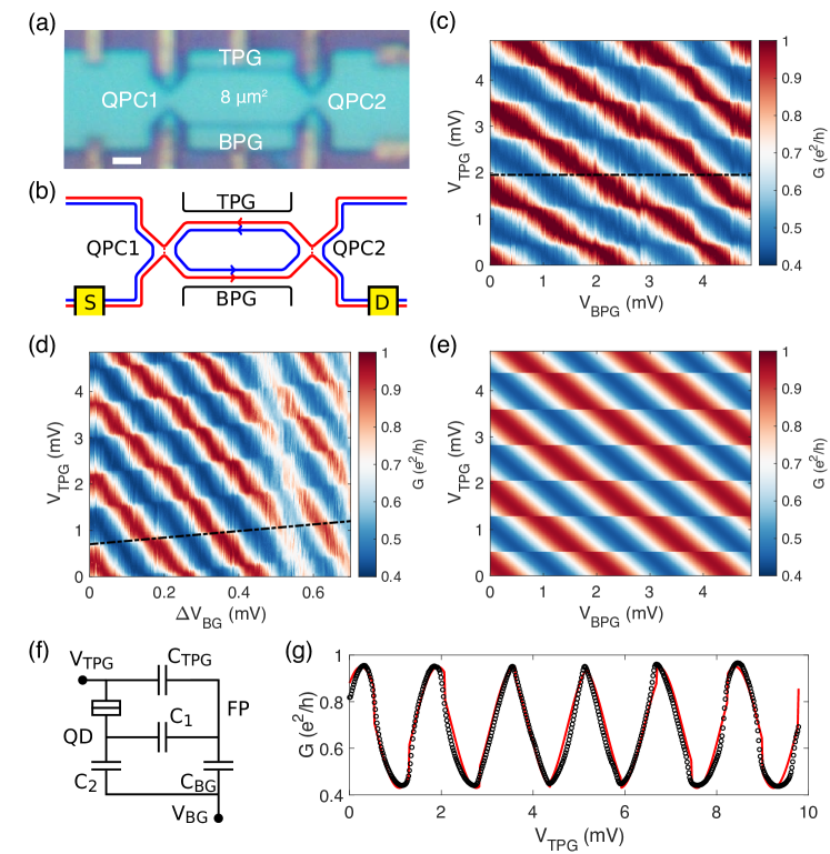
To further explore the operation of the graphene gates, we designed a Fabry-Pérot interferometer using QPC1 and QPC2, which both showed good quantization of the and 2 states at T (see Supporting Information Fig. S1). To this end, we etched nm wide trenches into the graphene region between QPC1 and QPC2, thereby detaching the two middle metal contacts that were used to measure Fig. 1. The advantage of severing the contacts is two-fold. First, the edge states that used to be equilibrated by these contacts can now preserve their phase coherence in the region between the two QPCs, thereby forming the interferometer, see Fig. 2(a). Second, the two graphene strips attached to the former contacts now serve as the top and bottom plunger gates (TPG and BPG). Voltages and applied to the plunger gates tune the positions of the quantum Hall edge states, which affect the effective area of the cavity between the two QPCs. The resulting interferometer cavity is about 8 in area and 12 m in perimeter.
We first study the case, when the interferometer has two distinct edge channels. The back-gate voltage is set at = 3.05 V, corresponding to the beginning of the bulk 2 plateau, which extends from 2.8 V to 6.8 V. The QPC voltages are fixed at 20 V and 8 V. Here, the inner channel is fully reflected while the outer channel is partially transmitted into the cavity and is the one causing the interference pattern, see schematics in Fig. 2(b). With these parameters, the transmission probabilities of the outer channel are estimated to be (see Supporting Information).
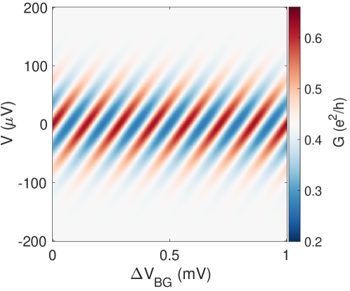
We start by applying voltages to both plunger gates; increasing these voltages moves the interfering channel towards the graphene edge, thereby increasing the enclosed area . If the magnetic field is held constant, a change in the area modulates the AB phase of electrons traveling around the cavity by . This modulation can be observed by measuring the differential conductance across the interferometer while tuning both and (Fig. 2(c)). We observe periodic interference fringes in a wide range of gate voltages, with similar periods of about 2 mV, indicating that the two gates have similar efficiency.
We next focus on the small phase jumps observed in Fig. 2(c) (one of them is marked by the black dashed line). The features are periodic in TPG, indicating regular charging of some localized states. The features are not affected by the BPG, resulting in their appearance as horizontal lines. Apparently, these states are located in the TPG region, and the BPG is too far away to have a sizable effect. In Fig. 2(d), we plot the same interference pattern as a function of TPG and BG. The features now acquire a slope vs. and (see the black dashed line as an example), which indicates that the states are influenced by both grates. In comparison to the AB fringes associated with the interferometer, these phase jumps appear twice more frequently in , but five times less frequently in (see the separation between jumps in Fig. 2(d)). Most importantly, their slope is positive, opposite to that of the AB fringes.
These observations suggest that the states responsible for the small phase jumps are localized not in the interferometer, but in the region of graphene attached to the TPG, which effectively forms a small quantum dot. The states in this dot are coupled to the gate electrode via tunneling, and applying positive TPG voltage depletes this dot of electrons, in contrast to the same voltage adding electrons in the interferometer. This is the reason why the resulting phase jumps follow lines of a positive slope in the plane of Fig. 2(d). The graphene region connected to TPG is about 4-6 times smaller than the interferometer, in agreement with the observed smaller capacitance of these states to the BG as compared to the states of the interferometer.
Once the origin of the phase jumps has been identified, it is straightforward to account for them by considering the capacitive network shown in Fig. 2(f). Here, the localized states in the TPG region (QD) are tunnel coupled to . Their capacitances to the interferometer (FP) and BG are and respectively. The capacitances of the interferometer to the TPG and BG are and . The amplitude of the phase jumps is given by . We approximate the oscillatory part of conductance by a simple appropriate for our relatively high base temperature of 100 mK where higher-harmonics have been sufficiently suppressed by thermal smearing effect (see the next section). In Fig. 2(g), we plot the conductance vs. TPG (dots), corresponding to the vertical cross-section on Figs. 2(c). The distortions of the oscillations introduced by the phase jumps are well captured by the fit (red line). The fit gives aF and . Using the parameters obtained in this fit, we can calculate the expected interference pattern. The resulting conductance pattern is shown in Fig. 2(e), demonstrating a good qualitative agreement with the experiment (Fig. 2(c)). From the period of the interference pattern mV and of the phase jumps mV in Fig. 2(d), we further estimate aF and aF. Therefore, we have aF and aF. We note that the BPG does not produce similar features, indicating that the metal electrode is better coupled to the nearby graphene region.
3 Energy dependence of conductance oscillations
We next explore the energy dependence of the interference fringes by tuning the temperature and bias. We chose to set the bulk filling factor at , when only a single spin-polarized edge channel is present. We plot the conductance pattern as a function of bias and in Fig. 3(a). The map shows contours of constant phase, which are sometimes interpreted as non-interacting AB oscillations, although it has been demonstrated that the charging effects are significant 21, 22 even at 23. We estimate (see Supporting Information) that in our case the charging energy exceeds the level spacing. In fact, the familiar Coulomb diamonds can be recovered by integrating the differential conductance to plot the current through the dot (Fig. S4). The diamonds are strongly asymmetric because the capacitance to the gates dominates the capacitance to the source and drain contacts. The vertical boundaries of the diamonds are not visible in the differential conductance but are revealed in the current map.
The strong role of the Coulomb interactions is confirmed by Fig. 3(b), which shows the map of conductance in the plane, where is the deviation of magnetic field from 6 T. The AB period of the interferometer should be mT, and on that scale the interference fringes show negligible slope, which indicates the dominant role of the charging energy 17. Similar nearly vertical conductance fringes were observed in the other measurement at dominated by Coulomb interactions 23.
Nonetheless, the description in terms of Fabry-Pérot interference is still possible. To that end, we average the conductance over the gate voltage, , as shown in the right inset of Fig. 3(a). We then subtract from the data in Fig. 3(a) and obtain a simple stripe pattern of Fig. 3(c), which strongly resembles the simulated conductance map of resonant tunneling plotted in Fig. S8. Note that the background subtraction does not affect the amplitude of conductance oscillations vs. .
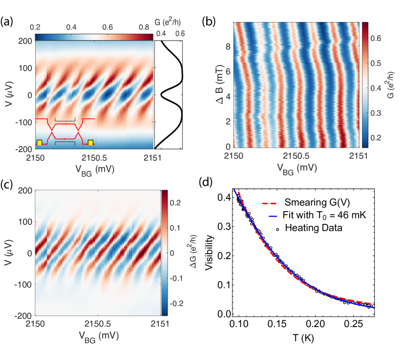
The conductance fringes in Fig. 3(c) have a positive slope, where increasing increases the AB phase , as we have seen in Fig. 2. On the other hand, increasing reduces the “traveling phase” , where is the perimeter of the interferometer and is the velocity of the edge states, which is renormalized by interactions. We use Fig. 3(c) to obtain the bias oscillation period of 80 V. From here, we estimate the edge state velocity 2.3105 m/s, which agrees with the previously reported values 5, 6.
The variation of the geometrical phase with energy results in smearing of the conductance pattern. We find that in our temperature range mK it is sufficient to approximate the conductance oscillations as . From here, we obtain the thermal dependence of the oscillations:
| (1) |
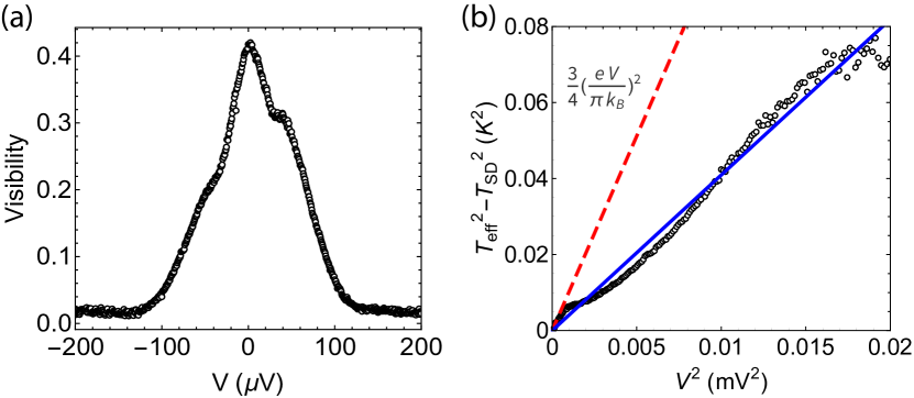
where is the Fermi distribution function and . Therefore, the visibility of the oscillations, defined as , is expected to be proportional to . To extract the visibility from the experimental data, we measure the conductance maximum (minimum) as the average height of several peaks (valleys) in measurement of Fig. S5. The resulting Fig. 3(d) shows the measured zero-bias visibility vs. temperature (black dots) and the fit (blue solid line). Note that the expression of Eq. (1) does not simply reduce to . The fit yields mK, which closely matches the value mK with the value of obtained from Fig. 3(c).
Another way to compare the energy and temperature scales is to numerically convolve the transmission extracted from the pattern in Fig. 3(a) with the Fermi-Dirac distribution at elevated temperatures. The result is shown as the red dashed line in Fig. 3(d), also agreeing with the measured temperature dependence. The fact that both numerical convolution of and fitting with Eq. (1) produce consistent results verifies that thermal broadening is the main origin of the visibility suppression at elevated temperatures.
In summary, we present a simple recipe to fabricate quantum point contacts with self-aligned side-gates in graphene, which operate in the quantum Hall regime. A reduction in the constriction widths of the QPCs improves their tunability at the expense of the degree of the conductance quantization, suggesting an optimal width in the nm range. We use this technique to define a quantum Hall Fabry-Pérot interferometer and explore the charging patterns both for and , studying their dependence on gate voltages, bias and temperature. In the future, additional screening layers such as top and bottom graphite gates can be used to reduce the charging effects 24. Such designs, pioneered in GaAs could enable exploration of the non-Abelian statistics in the fractional quantum Hall regime 25, 26. The quality of the side-gates and QPCs can also be substantially improved with emerging cryoetching 9 and AFM lithography 10, 7 techniques.
4 Methods
4.1 Sample Fabrication
The graphene and h-BN crystals are exfoliated onto SiO2 substrates and then assembled together by the conventional dry transfer technique using PC/PDMS stamps. The contacts and trenches are patterned by electron beam lithography using a layer of PMMA resist, developed in cold IPA/DI water mixture (ration 3:1) and then further etched by CHF3/O2 plasma in a reactive ion etcher. The Cr/Au (1 nm/100 nm) metal leads are deposited at 10-7 mbar base pressure in a thermal evaporator.
4.2 Measurement
The device is cooled down to the base temperature of mK in a Leiden dilution refrigerator wired with resistive coaxial lines and low pass filters. The two-terminal differential resistance of individual QPCs is measured with 1 nA, 15 Hz square-wave excitations with a digital acquisition board and a homemade voltage preamplifier. For a better signal-to-noise ratio, the two-terminal differential conductance of the interferometer is measured with a lock-in amplifier and homemade low noise current preamplifier with a current to voltage gain of 107. The amplitude of the voltage excitation applied from the lock-in amplifier is 7 V and the frequency is 577 Hz. In this case, the device is measured in series with two 5 kOhm filters, whose resistance is then subtracted from the measured resistance. Similarly, the voltage drop across the filters is subtracted from the applied bias to obtain the bias across the sample. By calibrating against the quantum Hall resistance of the sample, an overall gain correction of 1.0638 is obtained to account for the RC filters, voltage dividers and buffers used in the system. The DC bias and gate voltages are applied by a combination of NI USB-6363 and DAC8728 controlled by NI USB-6501.
We greatly appreciate stimulating discussion with H. U. Baranger. Transport measurements conducted by L.Z., E.G.A., and T.F.Q.L. were supported by NSF award DMR-2004870. Lithographic fabrication and characterization of the samples by L.Z. and A.S., as well as the project guidence by Z.I and G.F were supported by the Division of Materials Sciences and Engineering, Office of Basic Energy Sciences, U.S. Department of Energy, under Award No. DE-SC0002765. T.F. and F.A. were supported by a URC grant at Appalachian State University. K.W. and T.T. acknowledge support from the Elemental Strategy Initiative conducted by the MEXT, Japan, (grant no. JPMXP0112101001), JSPS KAKENHI (grant no. JP20H00354) and CREST (no. JPMJCR15F3, JST). The sample fabrication was performed in part at the Duke University Shared Materials Instrumentation Facility (SMIF), a member of the North Carolina Research Triangle Nanotechnology Network (RTNN), which is supported by the National Science Foundation (Grant ECCS-1542015) as part of the National Nanotechnology Coordinated Infrastructure (NNCI).
References
- Stern 2010 Stern, A. Non-Abelian states of matter. Nature 2010, 464, 187–193
- Carrega et al. 2021 Carrega, M.; Chirolli, L.; Heun, S.; Sorba, L. Anyons in quantum Hall interferometry. Nature Reviews Physics 2021, 3, 698–711
- Nakaharai et al. 2011 Nakaharai, S.; Williams, J. R.; Marcus, C. M. Gate-Defined Graphene Quantum Point Contact in the Quantum Hall Regime. Phys. Rev. Lett. 2011, 107, 036602
- Zimmermann et al. 2017 Zimmermann, K.; Jordan, A.; Gay, F.; Watanabe, K.; Taniguchi, T.; Han, Z.; Bouchiat, V.; Sellier, H.; Sacépé, B. Tunable transmission of quantum Hall edge channels with full degeneracy lifting in split-gated graphene devices. Nature Communications 2017, 8, 14983
- Déprez et al. 2021 Déprez, C.; Veyrat, L.; Vignaud, H.; Nayak, G.; Watanabe, K.; Taniguchi, T.; Gay, F.; Sellier, H.; Sacépé, B. A tunable Fabry–Pérot quantum Hall interferometer in graphene. Nature Nanotechnology 2021, 16, 555–562
- Ronen et al. 2021 Ronen, Y.; Werkmeister, T.; Najafabadi, D. H.; Pierce, A. T.; Anderson, L. E.; Shin, Y. J.; Lee, S. Y.; Lee, Y. H.; Johnson, B.; Watanabe, K. et al. Aharonov–Bohm effect in graphene-based Fabry–Pérot quantum Hall interferometers. Nature Nanotechnology 2021, 16, 563–569
- Cohen et al. 2022, 2204.10296. arXiv Cohen, L. A.; Samuelson, N. L.; Wang, T.; Klocke, K.; Reeves, C. C.; Taniguchi, T.; Watanabe, K.; Vijay, S.; Zaletel, M. P.; Young, A. F. Tunable fractional quantum Hall point contacts in graphene via local anodic oxidation of graphite gates. 2022, 2204.10296. arXiv; \urlhttps://arxiv.org/abs/2204.10296 (accessed Nov. 21, 2022)
- Pogosov et al. 2022 Pogosov, A. G.; Shevyrin, A. A.; Pokhabov, D. A.; Zhdanov, E. Y.; Kumar, S. Suspended semiconductor nanostructures: physics and technology. Journal of Physics: Condensed Matter 2022, 34, 263001
- Clericò et al. 2019 Clericò, V.; Delgado-Notario, J. A.; Saiz-Bretín, M.; Malyshev, A. V.; Meziani, Y. M.; Hidalgo, P.; Méndez, B.; Amado, M.; Domínguez-Adame, F.; Diez, E. Quantum nanoconstrictions fabricated by cryo-etching in encapsulated graphene. Scientific Reports 2019, 9, 13572
- Kun et al. 2020 Kun, P.; Fülöp, B.; Dobrik, G.; Nemes-Incze, P.; Lukács, I. E.; Csonka, S.; Hwang, C.; Tapasztó, L. Robust quantum point contact operation of narrow graphene constrictions patterned by AFM cleavage lithography. npj 2D Materials and Applications 2020, 4, 43
- Veyrat et al. 2019 Veyrat, L.; Jordan, A.; Zimmermann, K.; Gay, F.; Watanabe, K.; Taniguchi, T.; Sellier, H.; Sacépé, B. Low-Magnetic-Field Regime of a Gate-Defined Constriction in High-Mobility Graphene. Nano Letters 2019, 19, 635–642
- Coissard et al. 2022, 2210.08152. arXiv Coissard, A.; Grushin, A. G.; Repellin, C.; Veyrat, L.; Watanabe, K.; Taniguchi, T.; Gay, F.; Courtois, H.; Sellier, H.; Sacépé, B. Absence of edge reconstruction for quantum Hall edge channels in graphene devices. 2022, 2210.08152. arXiv; \urlhttps://arxiv.org/abs/2210.08152 (accessed Nov. 21, 2022)
- Stampfer et al. 2011 Stampfer, C.; Fringes, S.; Güttinger, J.; Molitor, F.; Volk, C.; Terrés, B.; Dauber, J.; Engels, S.; Schnez, S.; Jacobsen, A. et al. Transport in graphene nanostructures. Frontiers of Physics 2011, 6, 271–293
- Bischoff et al. 2015 Bischoff, D.; Varlet, A.; Simonet, P.; Eich, M.; Overweg, H. C.; Ihn, T.; Ensslin, K. Localized charge carriers in graphene nanodevices. Applied Physics Reviews 2015, 2, 031301
- Bischoff et al. 2016 Bischoff, D.; Eich, M.; Varlet, A.; Simonet, P.; Overweg, H.; Ensslin, K.; Ihn, T. Graphene nano-heterostructures for quantum devices. Materials Today 2016, 19, 375–381
- Seredinski et al. 2019 Seredinski, A.; Draelos, A. W.; Arnault, E. G.; Wei, M.-T.; Li, H.; Fleming, T.; Watanabe, K.; Taniguchi, T.; Amet, F.; Finkelstein, G. Quantum Hall–based superconducting interference device. Science Advances 2019, 5, eaaw8693
- Halperin et al. 2011 Halperin, B. I.; Stern, A.; Neder, I.; Rosenow, B. Theory of the Fabry-Pérot quantum Hall interferometer. Phys. Rev. B 2011, 83, 155440
- de C. Chamon et al. 1997 de C. Chamon, C.; Freed, D. E.; Kivelson, S. A.; Sondhi, S. L.; Wen, X. G. Two point-contact interferometer for quantum Hall systems. Phys. Rev. B 1997, 55, 2331–2343
- Dean et al. 2010 Dean, C. R.; Young, A. F.; Meric, I.; Lee, C.; Wang, L.; Sorgenfrei, S.; Watanabe, K.; Taniguchi, T.; Kim, P.; Shepard, K. L. et al. Boron nitride substrates for high-quality graphene electronics. Nature Nanotechnology 2010, 5, 722–726
- Bischoff et al. 2015 Bischoff, D.; Simonet, P.; Varlet, A.; Overweg, H. C.; Eich, M.; Ihn, T.; Ensslin, K. The importance of edges in reactive ion etched graphene nanodevices. physica status solidi (RRL) - Rapid Research Letters 2015, 10, 68–74
- Ofek et al. 2010 Ofek, N.; Bid, A.; Heiblum, M.; Stern, A.; Umansky, V.; Mahalu, D. Role of interactions in an electronic Fabry–Perot interferometer operating in the quantum Hall effect regime. Proceedings of the National Academy of Sciences 2010, 107, 5276–5281
- Sivan et al. 2018 Sivan, I.; Bhattacharyya, R.; Choi, H. K.; Heiblum, M.; Feldman, D. E.; Mahalu, D.; Umansky, V. Interaction-induced interference in the integer quantum Hall effect. Phys. Rev. B 2018, 97, 125405
- Röösli et al. 2020 Röösli, M. P.; Brem, L.; Kratochwil, B.; Nicolí, G.; Braem, B. A.; Hennel, S.; Märki, P.; Berl, M.; Reichl, C.; Wegscheider, W. et al. Observation of quantum Hall interferometer phase jumps due to a change in the number of bulk quasiparticles. Phys. Rev. B 2020, 101, 125302
- Nakamura et al. 2019 Nakamura, J.; Fallahi, S.; Sahasrabudhe, H.; Rahman, R.; Liang, S.; Gardner, G. C.; Manfra, M. J. Aharonov-Bohm interference of fractional quantum Hall edge modes. Nature Physics 2019, 15, 563–569
- Nakamura et al. 2020 Nakamura, J.; Liang, S.; Gardner, G. C.; Manfra, M. J. Direct observation of anyonic braiding statistics. Nature Physics 2020, 16, 931–936
- Willett et al. 2013 Willett, R. L.; Nayak, C.; Shtengel, K.; Pfeiffer, L. N.; West, K. W. Magnetic-Field-Tuned Aharonov-Bohm Oscillations and Evidence for Non-Abelian Anyons at . Phys. Rev. Lett. 2013, 111, 186401
Supporting Information
5 Characterization of QPC transmissions
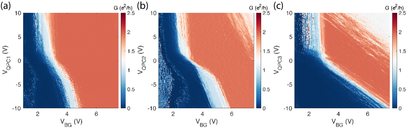
Before etching the device to form an interferometer, QPC1 and QPC2 are characterized at 6 T showing good quantization for (Fig. S1). Once the sample was etched to form the interferometer, the transmission coefficient of a particular QPC (1 or 2) can be estimated by measuring the two-terminal conductance of the interferometer, , while keeping the other QPC (2 or 1) open.
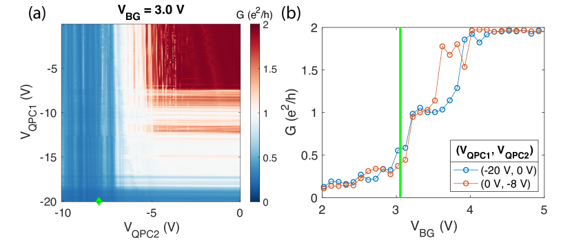
As shown in Fig. S2(a), we first measure as a function of both QPC voltages at V (). The green diamond marker labels the QPC operation point for Fig. 2 ( V and V). At V, both QPCs are open (). From the conductance at V and V, we find the QPC transmissions to be around 0.4 for both QPC1 and QPC2. For the data shown in Fig. 2, we use a slightly higher V and the QPC transmissions are found to be higher (see Fig. S2(b) where the green line marks V). Here, the estimation of QPC transmissions is and .
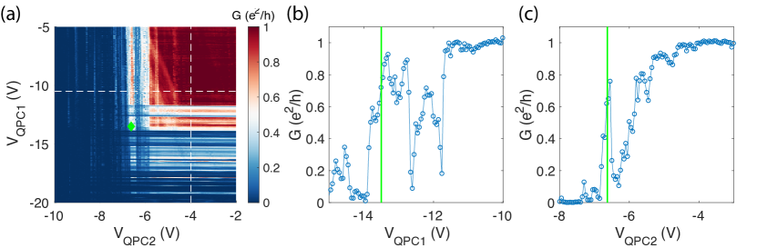
To determine the QPC transmissions at the operating point, in Fig. S3 (a), we plot as a function of both QPC voltages at the same back-gate voltage used in Fig. 3, i.e. V. The green diamond marker labels the QPC operation point for Fig. 3 ( V and V). Compared to , the QPC transmissions at are much more sensitive to the gate voltages, and the cross-talk between the two QPC gates becomes noticeable. In order to estimate the transmission of QPC1 more accurately in the presence of cross-talk, in Fig. S3(b) we plot as a function of at V, labeled by the vertical white dashed line in panel (a). This value of is not too far from the operation point, yet QPC2 is already open. Similarly, for determining transmission of QPC2, in Fig. S3(c) we plot a cut at V, corresponding to the horizontal white dashed line in panel (a).The QPC operation gate voltages labeled by green lines in panel (b) and (c), from which we estimate and .
Note that between measuring in the and regimes, the sample condition changed due to a sudden power-off of the electronics controlling the gates. Although the QPCs were still operating properly, the charge neutrality point shifted towards the p-side by V in .
6 Map of current through the interferometer
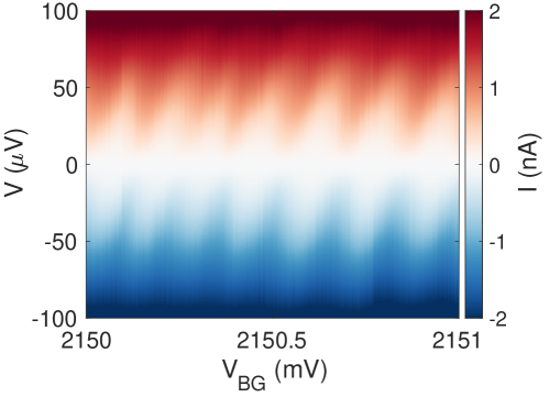
As demonstrated in Ref. 1, quantum Hall Fabry-Pérot interferometers have close relation to quantum dots in the quantum Hall regime. When the transmissions across the QPCs are high, the device is operated in the interferometer regime. Decreasing the transmissions gradually tune an interferometer smoothly into a closed quantum dot. Here, we operate the device in the intermediate regime. The close relation to a quantum dot can be seen in the map of the DC current through the interferometer as a function of the applied bias and the back-gate voltage, Fig. S4. This map is obtained by integrating the striped interference pattern of the differential conductance shown in Fig. 3a of the main text. “Coulomb diamonds” can be clearly seen in the center of the map and the size of the diamonds agrees with the oscillation period .
7 Interference pattern at higher energies and level spacing
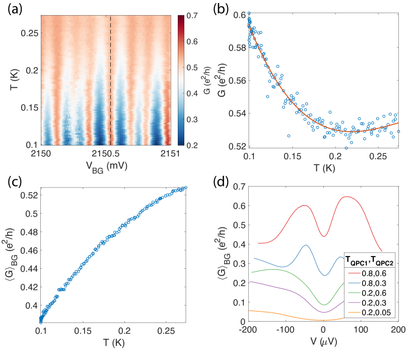
Fig. S5(a) shows the zero-bias conductance map vs. gate voltage and temperature, measured in the same range as Fig. 3 of the main text. In Fig S5(b), we plot the peak conductance as a function of temperature following the dashed line in panel (a). Clearly, the conductance maximum, , varies non-monotonically with increasing temperature. For K, decays with increasing temperature, as expected for transport through a single level. flattens and starts to increase above K, suggesting that multiple energy levels are contributing to the transport in this regime. Similarly, the contribution of the excited states is visible in the conductance averaged over gate voltage, , which grows with temperature, Fig. S5(c).
Finally, Fig. S5(d) shows measured vs. bias for several QPC configurations. In a Fabry-Pérot interferometer with negligible charging energy, should not depend on bias (neglecting dephasing), because the same levels are contributing to transport. Both here, and in Fig. 3(a), universally demonstrates a pronounced dip around zero bias. This dip is consistent with the observed increase with temperature (Fig. S5(c)), thereby providing an additional indication that multiple excited levels are involved.
We conclude that in our sample, the charging energy should dominate over the level spacing. This conclusion is consistent with the near lack of dependence in Fig. 3b.
8 Visibility decay at finite bias
In Fig. 3(a), we observe a rapid decay of the visibility of the interference pattern with increasing bias and the visibility becomes negligible above V, close to the oscillation period . Similar rapid decay of visibility with bias has been widely observed in both Fabry-Pérot and Mach-Zehnder interferometers, regardless of the hosting material. Unlike Mach-Zehnder interferometers, in Fabry-Pérot interferometers, it is hard to distinguish the effects of phase averaging and true decoherence. While the effects of decoherence can be modeled by an exponential or Gaussian decay 2, in the following we show that the observed suppression of visibility can also be phenomenologically attributed to an effective electron heating, resulting in phase averaging.
When weakly coupled to the source and drain leads, the non-equilibrium distribution function of the edge state in the interferometer, , is a weighted average of the distribution function of source and drain, and 3.
| (S1) |
where and () is the tunneling rate to the source (drain) proportional to the QPC transmissions. Strictly, this equation is only valid in the strong backscattering regime. But since it’s a continuous change from strong backscattering to weak backscattering, we use it as a crude approximation for the intermediate scattering regime studied here. For the case presented in Fig. 3, we use 1/2 since the estimated QPC transmissions are very close to each other ( and ). Without energy loss to the environment, - scattering tends to relax this non-equilibrium distribution into thermal equilibrium at elevated temperatures due to the excess energy in this double step distribution function 4. The effective temperature at full equilibrium is found to be 5
| (S2) |
where is the electron temperature of source and drain, is the applied voltage bias and is the Boltzmann constant. The second term under the square root is an effective heating from the relaxation of excess energy provided by the chemical potential difference. Since the edge channel likely does not achieve full equilibrium, we multiply this term by a parameter , which describes the amount of excess energy that has relaxed. Then, Eq. (S2) becomes
| (S3) |
One can relate the relaxation parameter to the electron-electron scattering rate via Boltzmann equation 6, which may depend on bias voltage. As shown in the main text, the visibility, , of AB oscillations in single-particle regime is proportional to to leading order. Therefore, at finite bias we have
| (S4) |
suggesting a fast decay of visibility with increasing bias.
To find the dependence of on , we use the relation between visibility and temperature obtained in Fig. 3(d) to convert the visibility at finite bias (plotted in Fig. S6 (a)) into an effective electronic temperature . Here, we symmetrize the visibility measured at positive and negative bias since the visibility decay is mostly independent from the small bias asymmetry observed in Fig. S6(a). In Fig. S6(b), we plot inferred from the visibility as a function of (black dots), together with from Eq. (S2) (red dashed line). First, we see that does not exceed , confirming that attributing the visibility drop to effective electron equilibration is not unreasonable. Second, is close to about 0.4 times (blue line), indicating that about 40 of the excess energy provided by the chemical potential difference is converted into thermal energy. Surprisingly, this fraction does not strongly depends on bias. Therefore, we find a bias independent that can well explain the finite bias visibility decay and from now on we treat it as a known constant for simulating the conductance map shown in Fig. 3(a).
Historically, the bias dependence of visibility of interference patterns has been fitted to either exponential decay 7 for Fabry-Pérot interferomters or Gaussian decay 8 for Mach-Zehnder interferometers. A comparison of both fits in Fabry-Pérot interferomters has been presented in Ref. 2, where both fitting expressions can capture the fast decay but not the exact trend. Here, Eq. (S3&S4) produces a Gaussian decay at low bias () and an exponential decay at high bias in agreement with the refined Gaussian phase randomization model presented in Ref. 9.
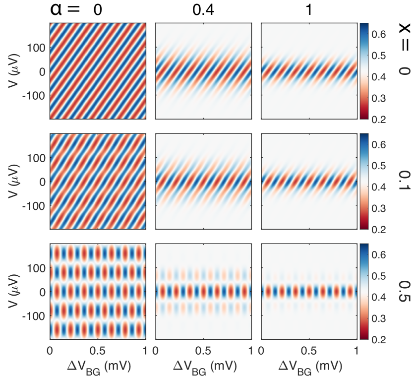
Next, instead of approximating the interference pattern as a sinusoidal function, we also want to take into account higher order terms and the bias symmetrization effect observed widely in prior works. Neglecting the renormalization of QPC transmissions which can give a power law modulation 10, the total current through the interferometer at zero temperature is
| (S5) |
where and . The distribution of the voltage drop is determined by the capacitive coupling between the interferometer and the source, drain, and gate electrodes. To take this effect into account, we follow Ref. 2 to set the source and drain bias drops as and . Therefore, the zero-temperature differential conductance at finite bias is
| (S6) |
where
| (S7) |
is the differential conductance contribution from electrons at energy .
The differential conductance at is then
| (S8) |
where
| (S9) |
To demonstrate the bias symmetrization effect together with the electron heating effect, we plot the calculated conductance maps for 0, 0.1, 0.5 and 0, 0.4, 1 in Fig. S7. As the voltage drop on drain increases, the pattern gradually evolves into a checkerboard. Meanwhile, increasing electron thermalization results in faster visibility decay at high bias. To simulate the background subtracted map shown in Fig. 3(c), in Fig. S8, we use , 0.1 K, 0.4 and 0. The map clearly reproduces the rapid decay of visibility above V seen in Figs. 3(a,c). Since there is no voltage drop on drain ( 0), the obtained interference pattern is stripe in contrast to the widely observed checkerboard pattern in GaAs. The checkerboard pattern corresponds to a symmetric voltage drop on source and drain due to the electrochemical potential of the cavity being tied to the source-drain voltages 10. Ref. 2 also observed a small voltage drop at the drain in a graphene interferometer of similar size and the effect of symmetrization increases with the interferometer size.
References
- Röösli et al. 2020 Röösli, M. P.; Brem, L.; Kratochwil, B.; Nicolí, G.; Braem, B. A.; Hennel, S.; Märki, P.; Berl, M.; Reichl, C.; Wegscheider, W. et al. Observation of quantum Hall interferometer phase jumps due to a change in the number of bulk quasiparticles. Phys. Rev. B 2020, 101, 125302
- Déprez et al. 2021 Déprez, C.; Veyrat, L.; Vignaud, H.; Nayak, G.; Watanabe, K.; Taniguchi, T.; Gay, F.; Sellier, H.; Sacépé, B. A tunable Fabry–Pérot quantum Hall interferometer in graphene. Nature Nanotechnology 2021, 16, 555–562
- Davies et al. 1993 Davies, J. H.; Hershfield, S.; Hyldgaard, P.; Wilkins, J. W. Current and rate equation for resonant tunneling. Phys. Rev. B 1993, 47, 4603–4618
- le Sueur et al. 2010 le Sueur, H.; Altimiras, C.; Gennser, U.; Cavanna, A.; Mailly, D.; Pierre, F. Energy Relaxation in the Integer Quantum Hall Regime. Phys. Rev. Lett. 2010, 105, 056803
- Altimiras et al. 2009 Altimiras, C.; le Sueur, H.; Gennser, U.; Cavanna, A.; Mailly, D.; Pierre, F. Non-equilibrium edge-channel spectroscopy in the integer quantum Hall regime. Nature Physics 2009, 6, 34–39
- Dubi and Sivan 2019 Dubi, Y.; Sivan, Y. “Hot” electrons in metallic nanostructures—non-thermal carriers or heating? Light: Science & Applications 2019, 8, 89
- McClure et al. 2009 McClure, D. T.; Zhang, Y.; Rosenow, B.; Levenson-Falk, E. M.; Marcus, C. M.; Pfeiffer, L. N.; West, K. W. Edge-State Velocity and Coherence in a Quantum Hall Fabry-Pérot Interferometer. Phys. Rev. Lett. 2009, 103, 206806
- Roulleau et al. 2007 Roulleau, P.; Portier, F.; Glattli, D. C.; Roche, P.; Cavanna, A.; Faini, G.; Gennser, U.; Mailly, D. Finite bias visibility of the electronic Mach-Zehnder interferometer. Phys. Rev. B 2007, 76, 161309
- Roulleau et al. 2008 Roulleau, P.; Portier, F.; Roche, P.; Cavanna, A.; Faini, G.; Gennser, U.; Mailly, D. Noise Dephasing in Edge States of the Integer Quantum Hall Regime. Phys. Rev. Lett. 2008, 101, 186803
- Dinh et al. 2012 Dinh, S. N.; Bagrets, D. A.; Mirlin, A. D. Nonequilibrium functional bosonization of quantum wire networks. Annals of Physics 2012, 327, 2794–2852