Edge audio devices can reduce data bandwidth requirements by pre-processing input speech on the device before transmission to the cloud. As edge devices are required to ensure always-on operation, their stringent power constraints pose several design challenges and force IC designers to look for solutions that use low standby power. One promising bio-inspired approach is to combine the continuous-time analog filter channels with a small memory footprint deep neural network that is trained on edge tasks such as keyword spotting, thereby allowing all blocks to be embedded in an IC. This paper reviews the historical background of the continuous-time analog filter circuits that have been used as feature extractors for current edge audio devices. Starting from the interpretation of a basic biquad filter as a two-integrator-loop topology, we introduce the progression in the design of second-order low-pass and band-pass filters ranging from OTA-based to source-follower-based architectures. We also derive and analyze the small-signal transfer function and discuss their usage in edge audio applications.
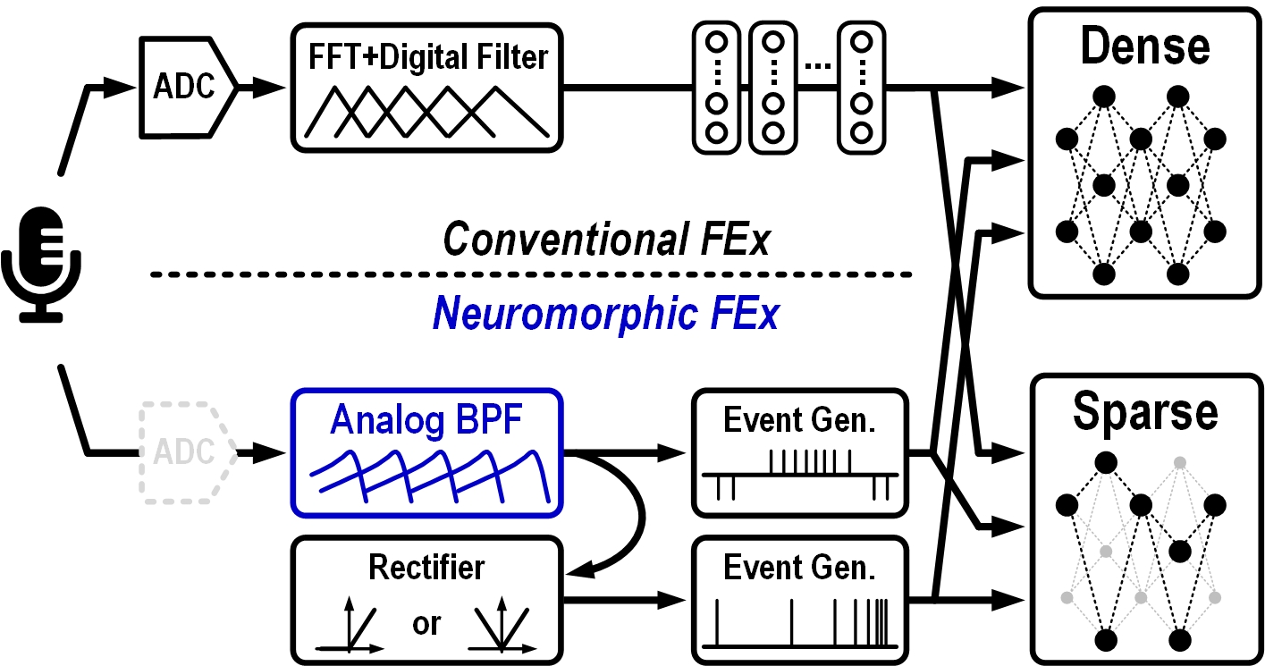
Edge audio devices are quickly gaining interest in the Internet of Things (IoT) domain, with particular focus on low-power devices that perform smart pre-processing of the input before data transmission to the cloud. Typical tasks performed on these devices include voice activity detection (VAD) and keyword spotting (KWS). As shown in Fig. 1, solutions for reported state-of-the-art edge audio integrated circuits (ICs) come in two forms. The first approach samples and quantizes the microphone output signal at Nyquist or oversampling frequency through an analog-to-digital converter (ADC). These data samples are then further processed by a digital signal processing block such as fast Fourier transform (FFT), followed by triangular filtering, and logarithmic compression.
The second approach is to replace the synchronous ADC and the subsequent signal processing stages with continuous-time (CT) analog circuits inspired by the biological modeling of cochleas [1]. These designs implement the frequency-selective filtering properties of the basilar membrane, rectifying properties of the biological inner hair cells, and neuronal firing of the ganglion cells [2, 3, 4, 5, 6, 7, 8, 9]. Since the FFT computation circuit is typically the most power-hungry building block of the entire audio feature extractor (FEx) [10], the analog signal processing has been regarded as a promising alternative in terms of better power efficiency [11, 12] thereby it could be useful for tasks implemented on low-power edge audio devices. The CT analog filters on the state-of-art edge audio ICs for VAD [13, 14, 15] and KWS [16, 17] adopt a set of second-order band-pass filters.
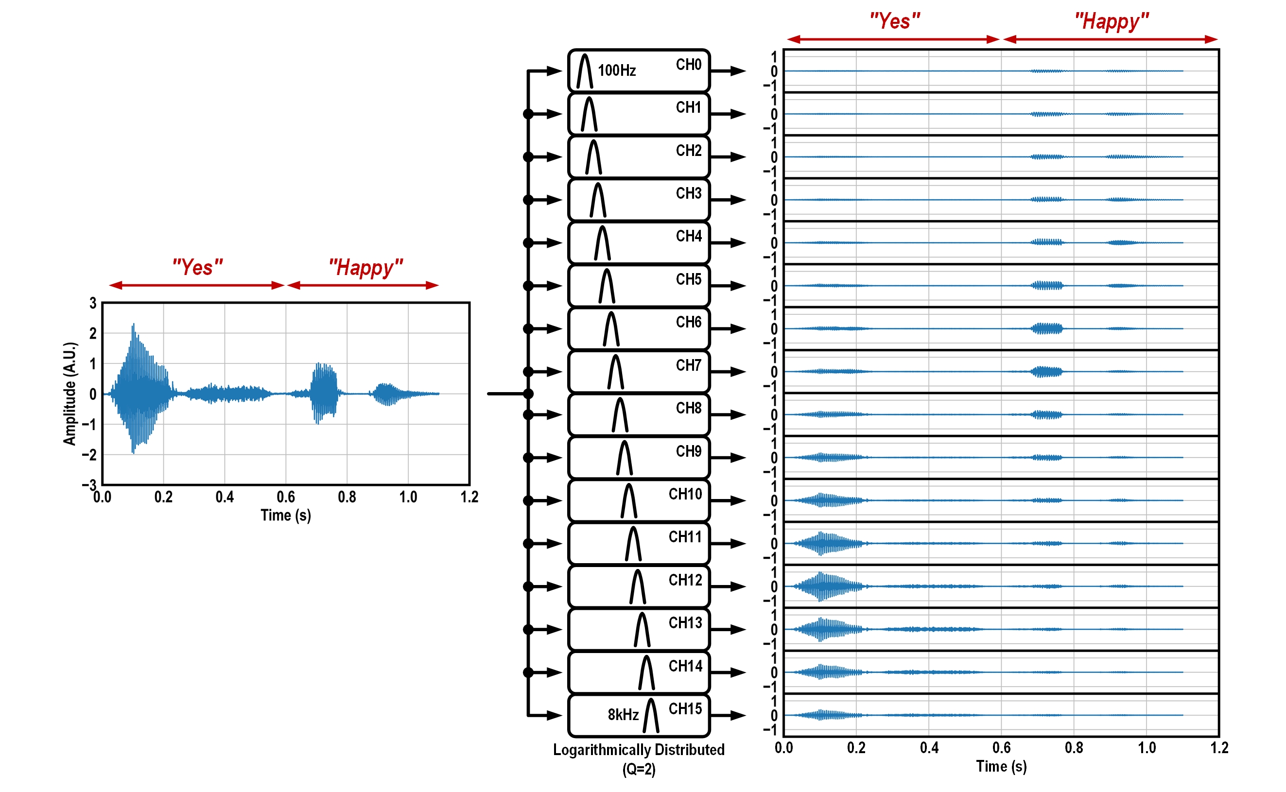
Fig. 2 shows an example of a CT audio processing stage. Here, a speech sample from the Google Speech Command Dataset (GSCD) [18] is fed to a 16-channel second-order Butterworth BPF bank [19]. It can be clearly seen that each channel responds to different parts of the speech sample depending on the instantaneous frequencies in the speech. These filter responses can be used for training a network on an audio task (see Fig 1).
Figure 1: Edge audio processing stages based on conventional and neuromorphic approaches [20, 21].Figure 2: Example of the output of 16 bandpass filter bank channels with center frequencies ranging from 100 Hz to 8KHz on a log-spacing and with . The audio input is an example speech from the GSCD samples.
This paper aims to provide an introductory survey of voltage-domain CT analog filters leading to the circuits that have been reported in recent edge audio ICs. It will provide a unified analysis that covers and small-signal equivalent diagrams, based on a two-integrator-loop biquad topology. To the best of our knowledge, it is the first work to present the operating principle of voltage-domain second-order filters using an unified analysis that includes the operational transconductance amplifier (OTA)-based, cross-coupled source-follower (XSF), super source-follower (SSF), and flipped voltage follower (FVF) biquad filters. Simulation results are also provided to show support for the proposed analysis. Note that the scope of this paper is geared to review transfer functions and thereby share intuitive circuit insights, rather than discussing every performance aspect of analog filter designs (e.g., noise, distortion, or sensitivity).
The remainder of this paper is organized as follows. Section II introduces the basics of biquad filters and discusses how a second-order BPF can be implemented from the two-integrator-loop topology. Section III presents the notation of a transconductor which is used in the description of the filters. Section IV and Section V present the core analysis of the OTA-based and source-follower (SF)-based filter circuits. Section VI summarizes and discusses the state-of-the-art approaches for the design of edge audio ICs with brief future research prospects. Section VII concludes this paper.
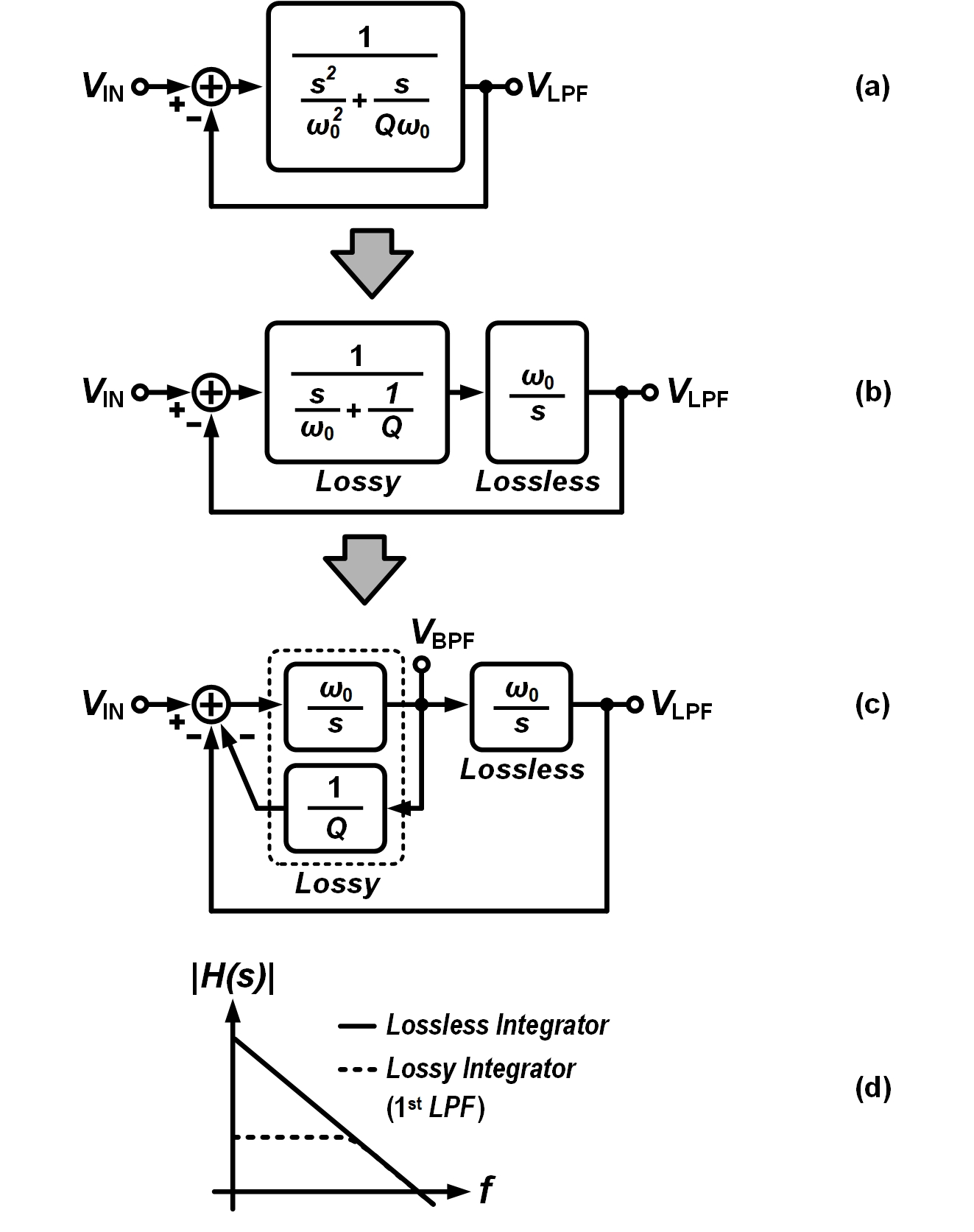
Figure 3: Two-integrator-loop representations of second-order LPF and BPF.
II Review on Biquad Filter
The second-order filter is also called as a biquadratic filter or a biquad filter. It is because its transfer function is the ratio of two quadratic equations.
Biquad LPF
The generic transfer function of a second-order LPF is
(1)
where is the natural frequency (also the cutoff frequency in LPF or center frequency in BPF) and is the quality factor of the filter.
We demonstrate how this transfer function can be decomposed into multiple forms that lead to different circuit topologies. We first express Eq. (1) in a similar form to the transfer function of the closed-loop gain of a negative feedback system, i.e., where is the feedforward gain, is the feedback gain.
By setting , and defining and as
(2)
we can construct a corresponding block diagram as shown in Fig. 3(a) where .
This topology can be further decomposed into a cascaded structure forming a Lossy integrator and a Lossless integrator as shown in Fig. 3(b) and is also called a Two-Integrator-Loop topology [22].
The characteristics of both integrator types are shown in Fig. 3(d). We see that the first-order LPF corresponds to the lossy case and an ideal integrator to the lossless case.
The lossy integrator can be further decomposed into a lossless integrator associated with a nested feedback path which controls of the second-order filter as shown in Fig. 3(c). This two-integrator-loop topology is used in a popular filter implementation called the Tow-Thomas biquad [23].
Biquad BPF with Poles at the Same Frequency
Fig. 3(c) also shows how a BPF response is obtained at the output of the lossy integrator within this topology. This is because the lossless integrator is excluded in the feedforward gain of compared to case, which in turn acts as a differentiation of (i.e., ). The transfer function of the resulting second-order BPF is expressed as
(3)
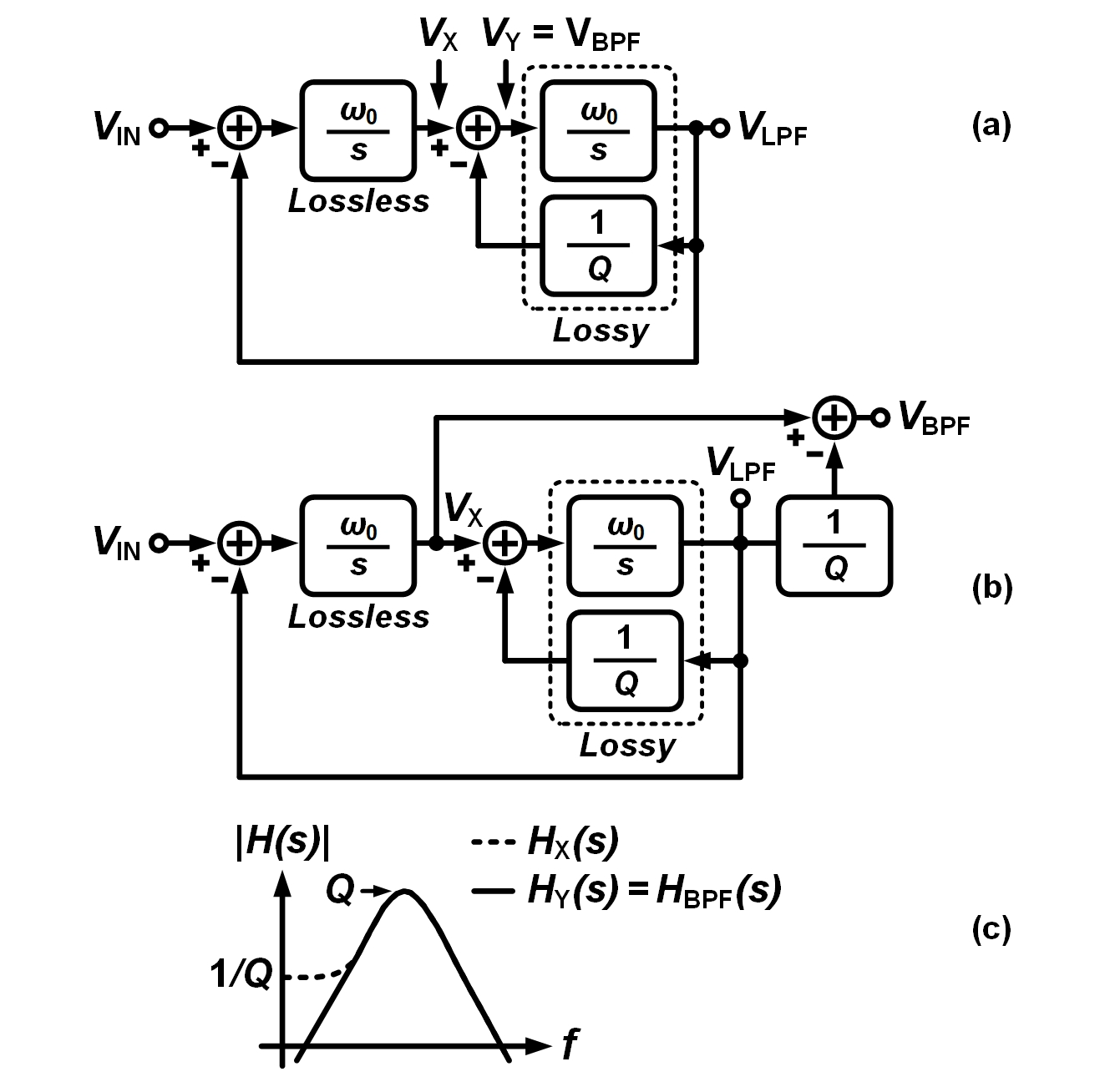
Figure 4: (a) Lossless-first two-integrator-loop, (b) design example of a BPF, and (c) frequency response of .
Fig. 4(a) shows a two-integrator-loop topology that uses a different configuration where the positions of the lossy and lossless integrators are reversed in contrast to the topology in Fig. 3(c). It is clear that the transfer function remains the same as in Eq. (1). This topology provides two additional output nodes, and . We first focus on the transfer function because the subtraction operation which leads to typically happens within the differential-input transconductors in the continuous-time filters
and thus cannot be extracted as an output. For example, corresponds to of the input transistor within the SF-based filters (see Section V-A). Exceptions are type-I SSF and type-I FVF filters, which will be discussed in Sections V-D and V-E. The transfer function , which is extracted from , the output of lossless integrator, deviates from the ideal BPF ( in Eq. (3)) response as an equation below.
(4)
Figure 5: Two-integrator-loop representations with a lossless-first configuration using two different poles.Figure 6: Second-order LPF composed of cascaded lossy integrators.
Fig. 4(c) shows that term incurs lossy high-pass response in . This lossy response can also be predicted by calculating , which gives , in contrast to the case where . To achieve an output with an ideal BPF ( in Eq. (3)) curve using the lossless-first two-integrator-loop filter, we can use (see Fig. 4(a)) where
(5)
Another method of getting a BPF output using the lossless-first two-integrator-loop topology is shown in Fig. 4(b). Here, and are subtracted, outside the feedback loop, to obtain as shown in (5).
Biquad BPF with Poles at Different Frequencies
We look next at the case where the filter has two different pole values (set by ) as in Fig. 5 instead of two identical poles (Fig. 4). The transfer functions corresponding to the nodes and the factor are described below.
(6)
Similarly to (4), includes term in the numerator and thus it exhibits a lossy behavior at its high-pass shape as shown in Fig. 5(c) where and its peak gain is . As in (5), by subtracting and , one gets an ideal band-pass response.
(7)
The subtraction can be implemented either within the feedback loop ( in Fig. 5(a)) or out of the loop ( in Fig. 5(b)). Note that term is not multiplied with in (7) because is now dependent on and while the feedback path within the lossy integrator in Fig. 5 has unity gain.
Figure 7: (a) The 4-port notation of a transconductor, (b) implementation of a lossy integrator with a transconductor, and block diagrams of a lossy integrator using (c) voltage-mode subtraction and (d) current-mode subtraction.Figure 8: OTA-based second-order LPF with (a) equivalent circuit and (b) small-signal diagram.
Biquad LPF with Cascaded Lossy Integrators
A second-order filter can alternatively be implemented by a cascade of two first-order lossy integrators with two different poles at () as shown in Fig. 6. The transfer function of this topology can be calculated as below.
(8)
The -factor of this topology has a maximum value of 0.5, which one can derive by using
. In order to realize a wide tunability, a second-order filter based on a two-integrator-loop topology is preferred over a cascaded lossy integrators.
In the following sections, we will analyze the second-order filter circuits by interpreting them either as lossy-first or as lossless-first two-integrator-loop topologies. In addition, we will only deal with the small-signal models excluding large-signal behaviors of the filter.
III Notation Declaration and Assumptions
Throughout this paper, transconductors () will be depicted using a 4-port drawing as shown in Fig. 7(a) [24], instead of the conventional 3-port drawing style that uses a single output port (rightside of Fig. 7(b)). This is particularly needed to analyze the source-follower-based filters, in which a single transistor acts as a transconductor and multiple transconductors are placed in a single bias current branch. We will discuss this type of filters in Section V. Fig. 7(b) shows an example of a lossy integrator implementation. The block diagram of this circuit can be described either with voltage-mode (Fig. 7(c)) subtraction or current-mode (Fig. 7(d)) subtraction. We will use both representations interchangeably.
We assume that the intrinsic gain of the transistor is sufficiently large, i.e., , where denotes the output impedance of a transistor, therefore, the load impedance of each transconductor can be approximated as . The body effect of the transistor is also ignored, i.e., .
IV OTA-Based Filters
IV-ASecond-Order LPF
Fig. 8 shows the OTA-based second-order LPF adopted in the early silicon cochlea designs [25, 4, 1, 26].
The circuit consists of 3 OTAs and 2 capacitors leading to a topology. Note that the diode-connected source degeneration technique was used in the OTAs of the feed-forward path (), to extend the linear input range of the filter [4] but at the expense of voltage headroom. The transfer function of this circuit is described below.
(9)
Figure 9: OTA-based second-order BPF [27] with (a) equivalent circuit and (b) small-signal diagram.
The basic structure of Fig. 8 is equivalent to the cascaded lossy integrators (or first-order LPFs) in Fig. 6. However, the added positive feedback makes a significant difference to the transfer function in (8) because it cancels out the negative feedback within the first lossy integrator when . It can be seen from the transfer function that cancels out when thereby the overall topology reduces to the lossless-first two-integrator-loop structure (see Fig. 5(a)). In other words, the positive feedback converts a lossy integrator into a lossless integrator. This in turn leads to complex poles in its transfer function and its maximum value is no longer limited to 0.5 in contrast to the case of cascaded lossy integrators (Fig. 6 and (8)). The transfer function, , and factor of the OTA-based LPF when are given below.
(10)
With this parameter setting, the positive feedback path is removed and thus the feedback stability is easier to be ensured.
In the original paper [1] that proposed the LPF in Fig. 8 for the cochlea channel, the following choices were made: and leading to the following equations for the transfer function, , and . The derived equation in (11) is the same as the one introduced in [1].
(11)
Compared to (10), this approach obtains and with simpler forms. In addition, it offers better matching since the same and are used for both the first and second lossy integrators. However, the positive feedback path is not removed and thus design parameters must be chosen carefully to ensure stability.
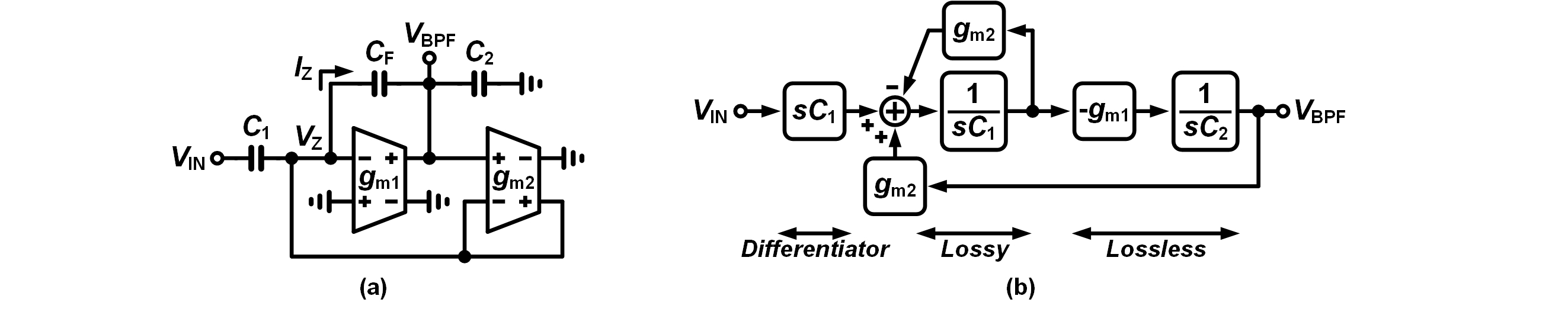
Figure 10: CCIA-based second-order BPF [13] with (a) equivalent circuit and (b) small-signal diagram.
IV-BSecond-Order BPF
Fig. 9 shows the implementation of an OTA-based BPF [27]. In addition to the original LPF in Fig. 8, a differential buffer takes the difference of the and . The buffer structure is equivalent to an open-loop first-order LPF (see Chapter 19 in [28]) or a lossy integrator, however its cutoff frequency is set by a parasitic capacitance . Note that the buffer is an open-loop design because the used transconductances for the feedforward () and feedback () paths are different.
This architecture follows the lossless-first two-integrator-loop topology with an external subtractor as discussed in Fig. 5(b). The transfer function of this OTA-based BPF is given in (12)
(12)
which can be derived using a nodal analysis in (13) where is given in (9).
(13)
Here, the approximation for is valid when the parasitic pole within the buffer stage is far higher than of the BPF and satisfying . This means that the buffer stage is assumed to have a sufficiently wide bandwidth. Note that and in (12) are the same as in (9) because the polynomial equation on the denominator does not change. Adopting the principle of this OTA-based BPF structure, further improved versions of the BPF [8, 5] that output a current-domain signal (excluding in Fig. 9) were implemented in a cascaded filter array. In [29], the fabricated filter circuit [5] was used as an audio FEx whose output was fed into a field-programmable gate array (FPGA)-based recurrent neural network (RNN) classifier for speech recognition task using the TIDIGITS dataset.
A simpler form of the BPF as shown in Fig. 10 uses the OTA as a core building block [13],[30].
This circuit adopts a capacitively-coupled instrumentation amplifier (CCIA) [31] associated with a buffer-based DC-servo loop. Its transfer function can be derived as in (14)
Here, we assume as used in [31]. We also assume the frequency range of this BPF is far lower than such that the filter parameters are solely determined by capacitors and transconductors. From Fig. 10(b), we see that this BPF circuit has a lossy-first two-integrator-loop topology shown in Fig. 3(c), with an added input differentiation stage . Therefore, although the block diagram might look like a second-order LPF, the transfer function shows a BPF response because of the differentiator. A parallel filter array adopting the BPF topology in Fig. 10 was implemented with an on-chip mixed-signal decision tree classifier in [13], and demonstrated a 2-class VAD task.
V Source-Follower-Based Filters
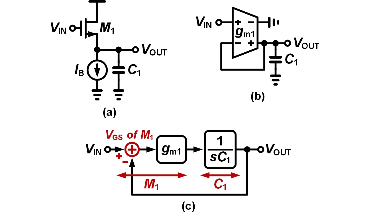
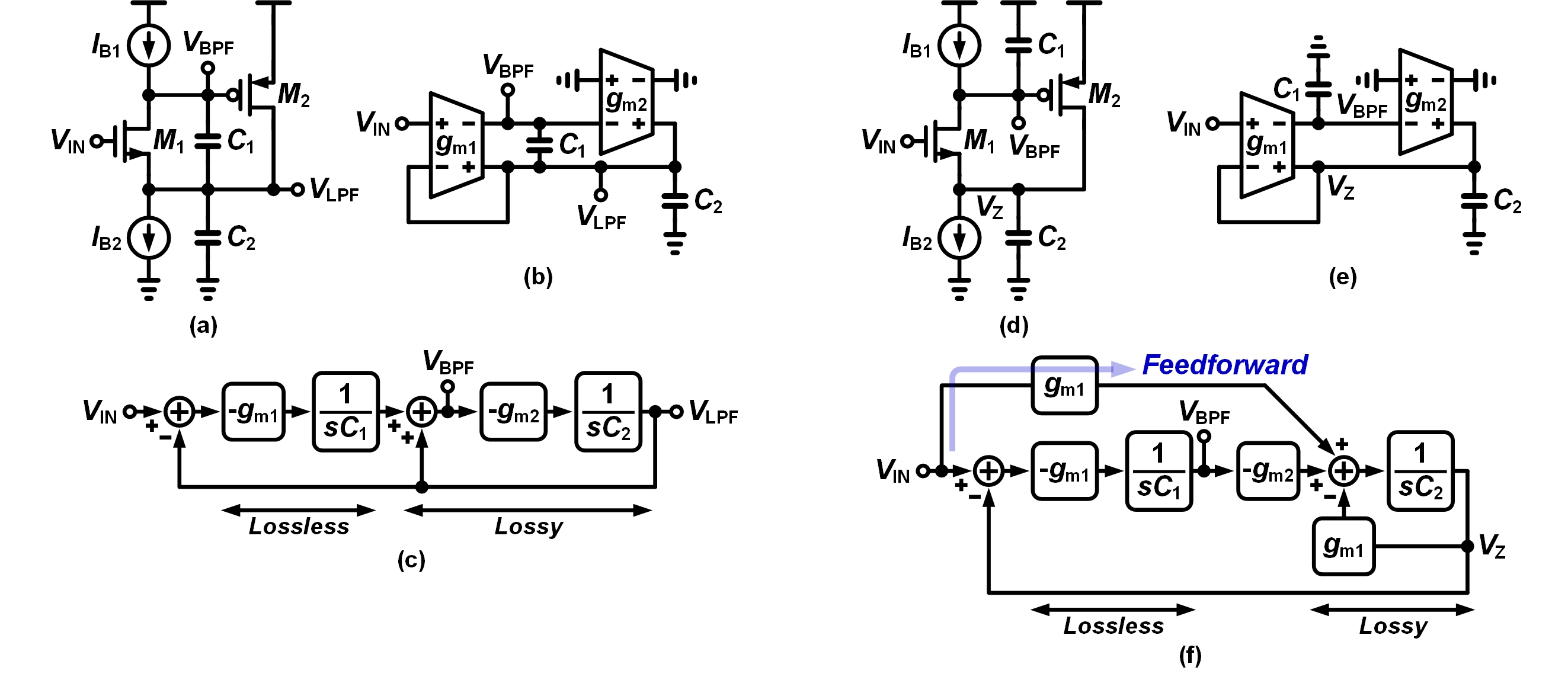
V-ASource-Follower (First-Order LPF)
Fig. 11 shows a transistor-level schematic, equivalent circuit, and block diagram of the SF-based first-order LPF. The minus output port (sink) of transconductor, which is the transistor, is tied to AC GND (corresponding to VDD in the schematic) in the equivalent circuit. The transfer function of the SF-LPF is given as below, denoting the equivalent transconductance of the circuit as (see Chapter 3.2.5 in [32]).
(16)
(17)
Figure 11: (a) Schematic, (b) equivalent circuit, and (c) small-signal diagram of the source-follower-based first-order LPF.Figure 12: (a) Transistor-level schematic, (b) half-circuit representation of the schematic, (c) equivalent circuit, and (d) small-signal diagram of the cross-coupled source-follower-based LPF.
(18)
Here, is the output impedance of transistor , is the output impedance of tail current source, and is the load impedance seen at the node. The approximation in (17) is valid assuming sufficiently large intrinsic gain of the transistor (). Since its cutoff frequency includes transconductance and capacitance, the SF-LPF is a first-order gmC filter or a lossy integrator as discussed in Section II and presented in Fig. 7(b). As shown in Fig. 11(b), the SF implements a local feedback around the source node of the transistor. Because the closed-loop gain at DC is given in the first term of (16), we can derive a DC loop gain of the local feedback in the SF, using the equation of closed-loop gain in the negative feedback system where and are used considering the unity-gain nature of the SF.
(19)
The above equation shows that the closed-loop gain approaches 1 as . In other words, the linearity performance of a SF-LPF is enhanced with a larger transconductance benefiting from its local feedback. Compared to the conventional open-loop gmC filters in which the input transistors are usually operated at strong-inversion to suppress harmonic distortions [28], the SF-LPF allows the input transistor to operate in subthreshold. Since the subthreshold region offers a higher within a given power budget, i.e., higher , the SF-based filters can be a promising option in terms of linearity-noise trade-offs. Note that the active RC filters also operate with a negative feedback loop thereby offering higher linearity than open-loop gmC filters, however they have a higher power burden because of the needed amplifiers to drive resistive loads [28]. Overall, the SF filters are more suitable for ultra-low-power audio filter implementation.
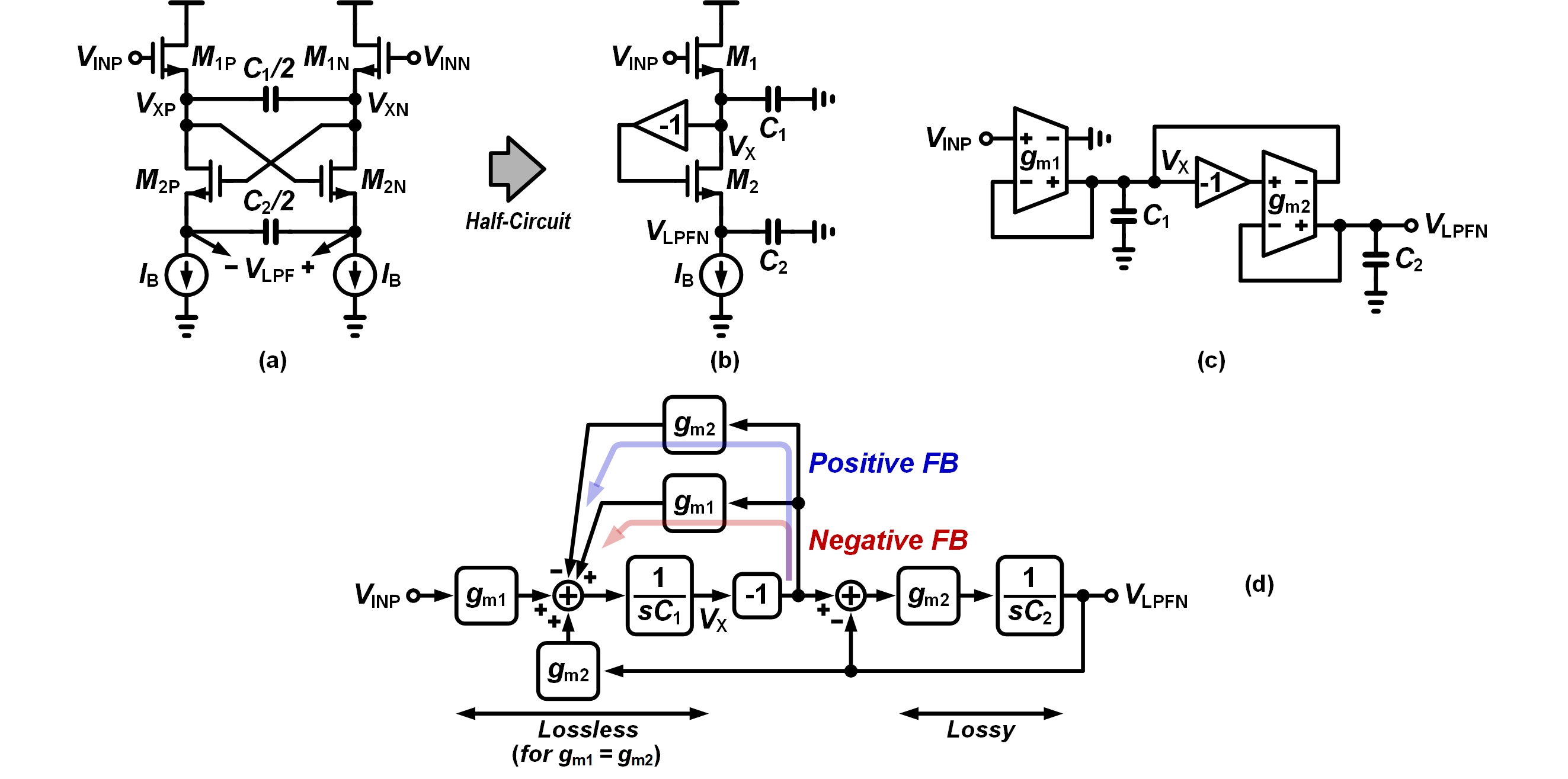
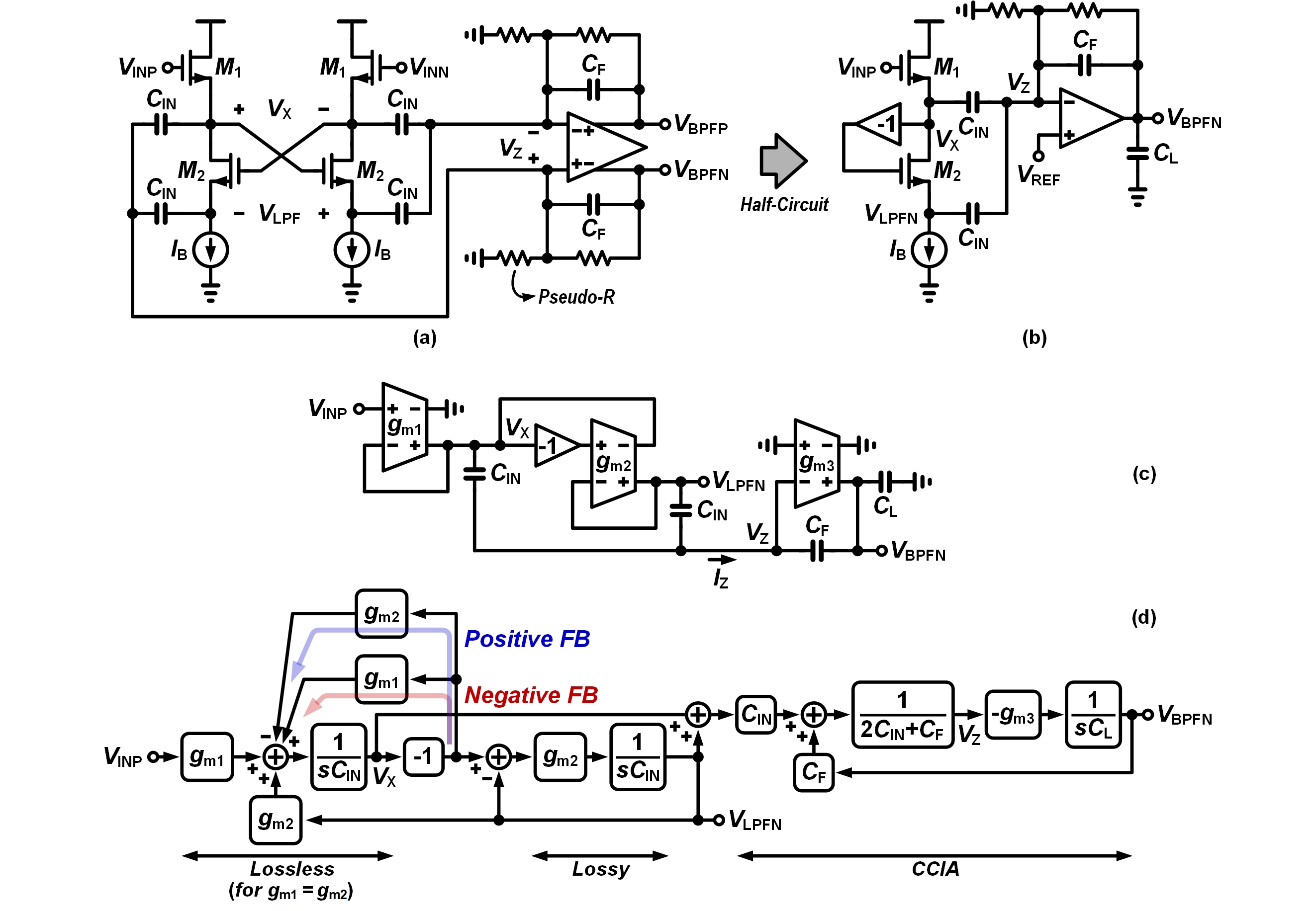
Fig. 12 shows a transistor-level full schematic, half-circuit equivalent, equivalent, and block diagram of the XSF-based second-order LPF [33, 34] while the transfer function and filter parameters are given in (18). Note that we define the polarity of the LPF output in a reversed way due to the cross-coupled structure within the filter circuit. For instance, the signal flow starting from ends at through the source-following operations of and . If we would like to extract the output from the left-half of the circuit () while also keeping the input fixed to the left-half (), an ideal inverting buffer is required considering differential structure of the circuit, as shown in the half-circuit schematic Fig. 12(b).
Although not easy to identify, interestingly, the core structure of this filter circuit is the same as the OTA-based LPF in Fig. 8, i.e., it has a lossless-first two-integrator-loop topology with auxiliary positive and negative feedback paths. Assuming as used in the original paper [33], the transfer function, , and of XSF filter are given below:
(20)
This equation becomes quite similar to the transfer function of the OTA-based LPF assuming in (10).
Figure 13: A step-by-step procedure for implementing the cross-coupled source-follower-based filter.
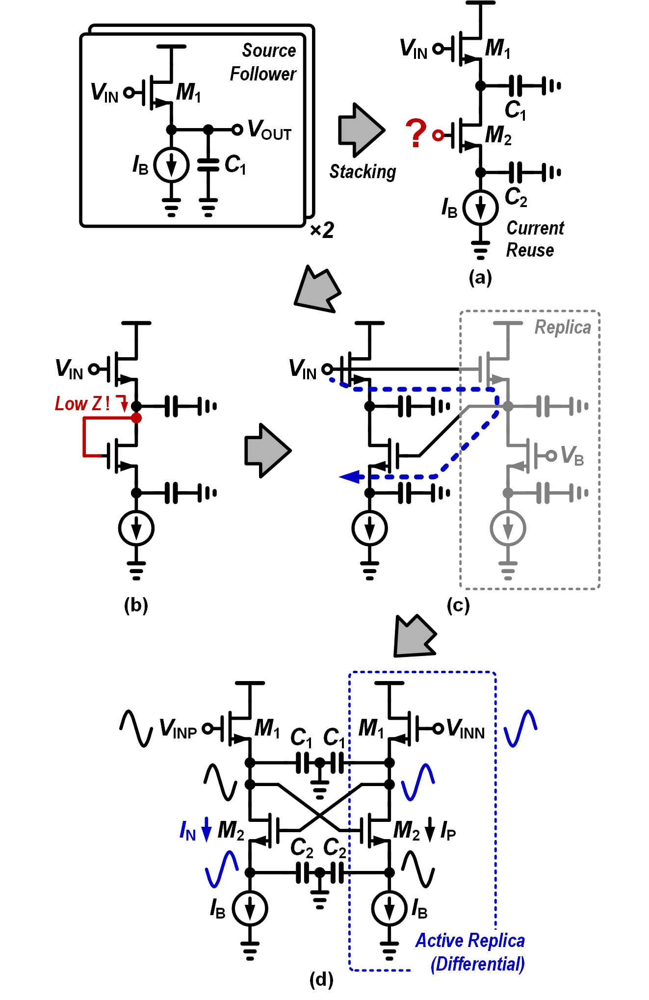
To provide an intuitive insight into the operation of the XSF circuit, a step-by-step design procedure starting from a basic SF is illustrated in Fig. 13. First, let us consider the case of stacking two SFs in a single branch. The stacking is especially beneficial as it allows a better matching and easier cut-off frequency tuning, because the bias current of the two SFs are reused. However, if the two SFs are stacked, the input of the second SF should be connected to the output of the first SF, which in turn, requiring gate and drain ports of input transistor in the second SF to be shorted into a single node. It results in a diode-connection of the input transistor as shown in Fig. 13(b), which incurs a low-impedance load to the first SF output, thereby leading to a failure of proper source-following operation of the first SF. One possible solution to this problem is using a replica SF (Fig. 13(c)). Here, input of the main circuit goes to the input of the replica circuit and we assume that the gate of the transistor in replica circuit is properly biased (). Note that the output of the first SF now has a cascode current source which is a high-impedance load. Therefore, the output of the second SF forms a cascaded lossy integrator (the blue line in Fig. 13(c)) as discussed in Fig. 6. Finally, we can exploit this replica circuit as an active building block that operates in a complementary manner to the main circuit, i.e., differential circuit, using a cross-coupling technique. The final schematic of the XSF is drawn as in Fig. 13(d). Note that the added positive feedback path (uppermost in Fig. 12(d)) cancels lossy property of the first SF within the cascaded lossy integrator and thus the maximum value is no longer limited to 0.5, as discussed in Section IV. We can omit the GND connection between the two capacitors and merge them into a single capacitor like in Fig. 12(a) because the input signal is in differential-mode and thus a virtual GND forms when in Fig. 12(a) is splitted into the two serialized .
(21)
The transfer function for node is derived as in (21). As discussed in Fig. 5(a) and (6), exhibits a lossy behavior at its low-frequency band.
Figure 14: Simulated frequency response of the XSF filter.Figure 15: (a) Transistor-level schematic, (b) half-circuit representation of the schematic, (c) equivalent circuit, and (d) small-signal diagram of the cross-coupled source-follower-based BPF [35].
(22)
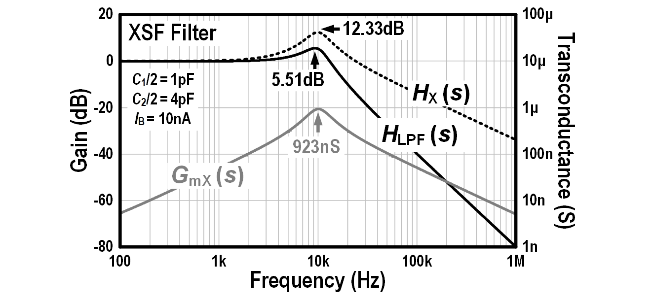
To evaluate the frequency response at and the analysis discussed in Fig. 5 and (6), an AC simulation is conducted with XSF filter circuit using a 65-nm CMOS process. The width and length of all transistors are sized at 1 .
The supply voltage is set as 1.2 V. Also, high devices are used since they have higher intrinsic gain than nominal devices. The source and body contacts of the transistors are shorted to negate body effects (a deep N-well layout is required in this case), therefore and (21) becomes valid. We will use the same simulation setups in Sections V-D and V-E unless otherwise it is specified. We set such that . Fig. 14 shows frequency responses of where
(23)
stands for the transconductance of differential current flowing through transistor in Fig. 13(d). As expected, shows a second-order LPF behavior with a 40dB/dec roll-off while has a band-pass characteristic but having a lossy behavior on its low-frequency band. Since we have designed , the peak gain is expected as according to Fig. 5 which closely matches to in our simulation result. The plotted graph shows a BPF response which corresponds to the output of within the lossy integrator in Fig. 12(d), as also discussed in (7). This is because the node in (7) corresponds to the output of the second subtractor in Fig. 12(d). As the extracted DC operating point in our simulation shows , the peak value of frequency response in is expected as where is considered according to (6, 7). This estimation also makes a close agreement with from our simulation result. The center frequency can be estimated using (18) as follow,
(24)
which also makes an agreement with from the simulation result in Fig. 14. The residual estimation errors may come from parasitic capacitance and insufficient as discussed in (19).
Similarly to Fig. 9 [27], a BPF architecture with an external subtractor applied to a XSF was proposed in [35] as shown in Fig. 15. We use the same XSF circuit from Fig. 12 to describe the operating principle for consistency, despite a folded input stage was used in [35]. The circuit uses a CCIA [31] to subtract from . The input ports of the OTA () within a CCIA works as a virtual GND by the negative feedback. Therefore, the virtual GND nodes that also exist in the XSF (see Fig. 13(d)) can be reused. In effect, capacitors in Fig. 15(a) contribute to the following: (1) filtering capacitors of the XSF; (2) input capacitors of the CCIA. The XSF circuit uses to realize equation within the CCIA, otherwise it forms a weighted addition, i.e., . We assume that the resistance of the pseudo-resistor is sufficiently large such that the associated AC-coupling high-pass cut-off frequency stays far smaller than in BPF. This allows us to omit pseudo-resistors in a small-signal equivalent circuit shown in Fig. 15(c). Based on the nodal analysis below, we can derive the transfer function of the CCIA .
(25)
where represents a small-signal current in Fig. 15(c), is a load capacitance of the CCIA. We assume and for the first approximation in (25). We can see that the bandwidth of CCIA is reduced by the amount of feedback factor from the original OTA bandwidth , as also described in [31]. The second approximation used in (25) is valid when the bandwidth of CCIA is sufficiently higher than in the BPF. The transfer function of the XSF-based BPF is derived in (22) using the equations as below. can be found in (18) but with an additional condition of .
(26)
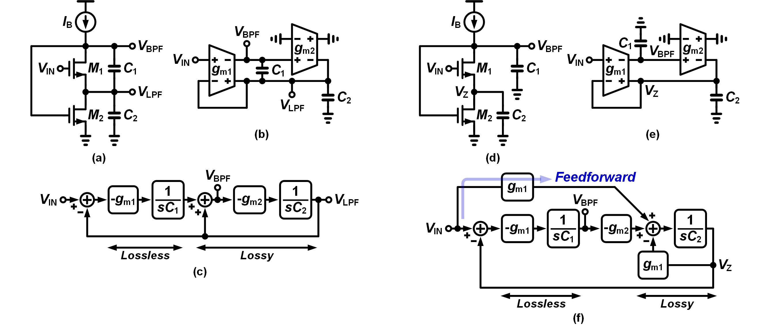
Figure 16: (a) Transistor-level schematic, (b) equivalent, and (c) small-signal diagram of type-I SSF [36] and (d) transistor-level schematic, (e) equivalent, and (f) small-signal diagram of type-II SSF [14].
(27)
(28)
A clear advantage of the SF-based filters over the OTA-based is its minimal number of parasitic poles. As shown in Fig. 12(a), the XSF filter exploits every node with the circuit as a source for pole synthesis while the OTA-based circuit does not. For instance, the mirror pole in the OTA acts as a non-dominant pole thereby necessitating additional power dissipation to uphold the same bandwidth as in the SF filter. A parallel filter array adopting the XSF-based BPF was implemented in [35]; and was used in an environmental sound classification task [37] and a 2-class speech versus noise task [38] with an FPGA environment.
Figure 17: Simulated frequency responses of the SSF filter.
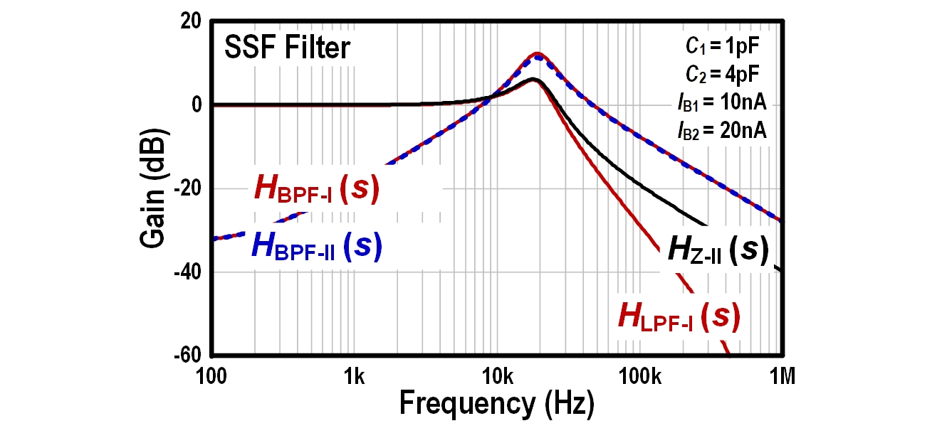
V-DSuper Source-Follower (Second-Order LPF/BPF)
Fig. 16 shows a schematic, equivalent, and block diagram of the super source-follower (SSF)-based filter circuits. As Fig. 16(a) and (d) show, the SSF filter can be categorized into two different types depending on how the capacitor is connected: (1) bootstraps and in type-I; (2) is connected to but its other plate is shunted to GND in type-II. In both types, the basic structure follows the lossless-first two-integrator-loop topology as discussed in Fig. 5(a). However, the type-II SSF incorporates a feedforward path. The transfer functions and filter parameters of type-I and type-II SSF filters are summarized in (27, 28). Interestingly, both SSF types can be deployed as a BPF without requiring any external subtractor in contrast to the OTA-based (see Fig. 9) and XSF-based (see Fig. 15) BPFs. For the type-I SSF, this is because bootstraps and within the lossless integral operation. In other words, the resulting small-signal voltage difference, i.e., , is generated on top of the node. In effect, the is located after the second subtractor which receives as an operand, thereby corresponds to in Fig. 5(a). Note that the small-signal current generated from the transconductor does not contribute to the voltage difference over the capacitor since the source and sink ports of the transconductor are all tied to both plates of the capacitor. Assuming sufficiently large output impedance of the transistors, the small-signal current generated from the transistor flows entirely into the capacitor, resulting that the generated small-signal current is trapped within the loop (used in (30)). A similar phenomenon can be found in the noise contribution of cascode devices (see Chapter 7.4.4 in [32]). A nodal analysis for calculating (27) according to Fig. 16(b) is given as below.
(29)
(30)
For type-II SSF, the key enabler for achieving the BPF response is the feedforward path. As discussed in (6) and Fig. 5(b), within the lossless-first two-integrator-loop topology has a lossy low-frequency behavior. However, the gain path from to for calculating the transfer function includes two different paths: (1) direct path ; (2) loop around path where . Since both paths have different polarities, they cancel out each other so that the lossy term in the numerator of (6), i.e., , is eliminated. A nodal analysis for calculating (28) according to Fig. 16(e) is given as below.
(31)
(32)
Note that unlike type-I SSF, the remaining node () does not show a second-order LPF response. The transfer function of the type-II SSF is given as below.
(33)
Since the transfer function has 1 pole in the numerator and 2 poles in the denominator, similarly to in (6), it effectively shows a first-order low-pass response.
Figure 18: (a) Transistor-level schematic, (b) equivalent, and (c) small-signal diagram of the type-I flipped voltage follower [39] and (d) transistor-level schematic, (e) equivalent, and (f) small-signal diagram of the type-II flipped voltage follower [15].
(34)
(35)
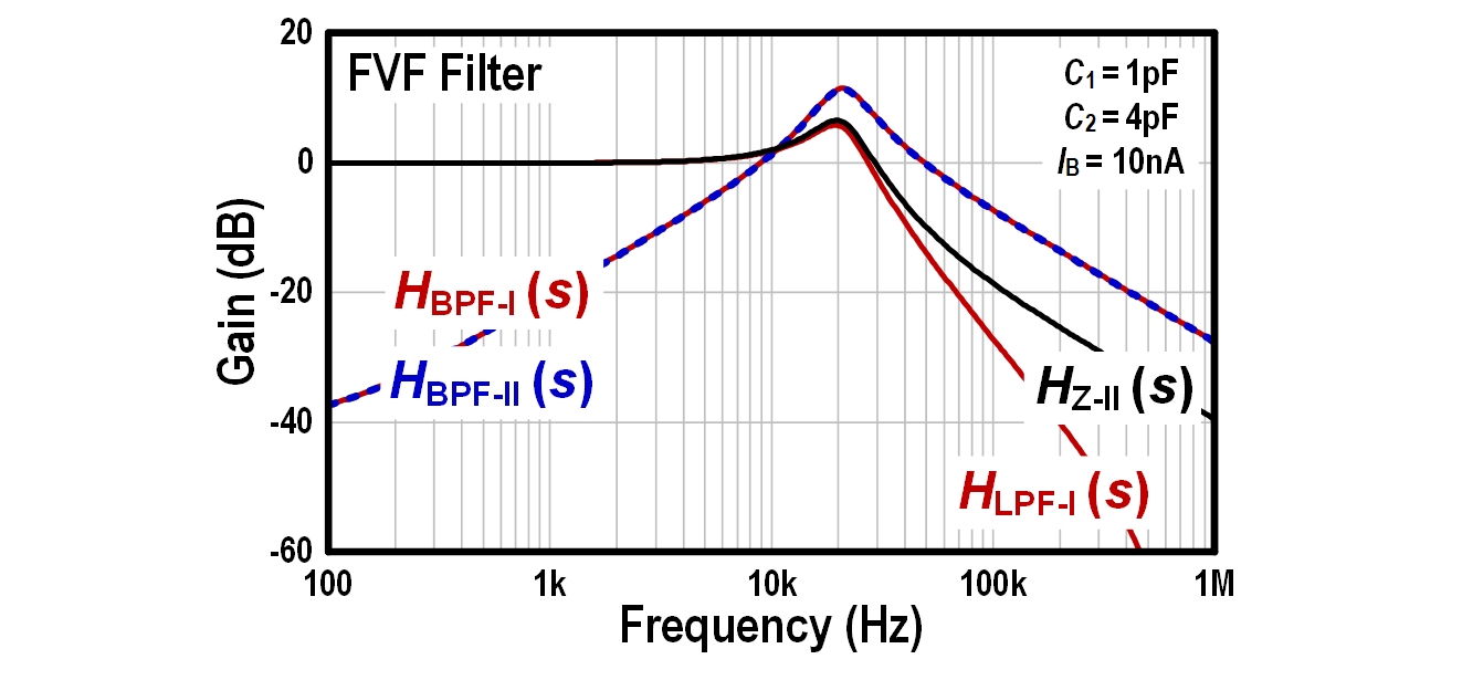
Figure 19: Simulated frequency responses of FVF filter.
Our analysis on the type-I and type-II SSF filters are verified with an AC simulation as shown in Fig. 17. We set such that the same bias currents are distributed to / transistors. Therefore, the transconductances for both transistors are closely set. and . Note that we keep the capacitance ratio as same as the XSF filter simulation shown in Fig. 14, thereby can be designed as . The other simulation setups are the same as mentioned in Section V-B. As predicted in (27, 28), Fig. 17 shows that both type-I and type-II SSF filters when they are probed at have BPF responses. Their peak gains are and for type-I and type-II cases respectively, and close to our estimated value of , which is also described in the XSF filter simulation. The simulated peak gain values of the two filters are different because the theoretical equations are different as given by (27, 28) considering slightly different values for /. A second-order low-pass roll-off is observed with and a first-order roll-off with .
The center frequencies of type-I/type-II SSFBPFs can be estimated using (27, 28) as below.
(36)
which makes a close agreement with from the simulation result in Fig. 17. The type-II SSF-based BPF was implemented within a channel of a parallel filter bank feature extractor in [14]. Together with an on-chip multilayer perceptron (MLP) classifier, it implemented a VAD.
V-EFlipped Voltage Follower (Second-Order LPF/BPF)
Fig. 18 shows a schematic, equivalent, and block diagram of the flipped voltage follower (FVF)-based filter circuits [40]. The FVF circuit has been actively used as a core building block in various analog circuits to name, such as LPF [39], low-dropout (LDO) regulator [41, 42, 43], bio-signal amplifier [44, 45, 46, 47, 48, 49], and current driver [50, 51]. As of the case in the SSF filters, the FVF filters are also categorized into two types according to the connection methods of capacitor. Interestingly, the equivalent circuits of the SSF and the FVF are the same except for the input polarity of transconductor (pFET gate in SSF, nFET gate in FVF). Since the inversion characteristic of transconductor still does not change, resultant block diagrams of the SSF and FVF are exactly same regardless of whether they are type-I or type-II. Therefore, the transfer functions of FVF filters described in (34), (35) are also the same as of the SSF filters (27), (28).
Fig. 19 shows an AC simulation result of the type-I and type-II FVF filter circuits. We set and the resulting transconductances are and . The other simulation setups are the same as XSF in Section V-B and SSF in Section V-D. As expected, the transfer curves for , , , and show the same characteristic as we observed in the SSF simulation result (Fig. 17). The peak gains of type-I and type-II BPFs are and respectively, where their center frequency is observed as . The simulated filter parameters are in close agreement with our estimation using (34) and (35), and
(37)
A significant advantage of the FVF over the SSF is its power efficiency in terms of bandwidth. More specifically, as shown in Fig. 17 and Fig. 19, the FVF consumes 2 less current () while the SSF consumes to achieve for . This is because the tail current in the SSF is divided into two different bias currents, and , for and respectively. On the contrary, the FVF exploits its inherent current reusing nature to save the power. More importantly, the FVF circuit offers better matching over the SSF, not merely because of the single branch biasing, but also of the same transistor type. For example, and transistors are all nFET in the FVF while it is not the case in the SSF. As a result, the FVF circuit is more robust over process variation because it is difficult to match different transistor types especially in regards to the shallow trench isolation (STI) and well proximity effect (WPE) [52]. The type-II FVF-based BPF was implemented as a parallel audio FEx for a VAD integrated circuit (IC) in [15].
TABLE I: Summary of audio FEx and their usage for edge audio intelligence
AThis number includes power consumption of the microphone pre-amplifier and test circuits.
BEstimated from chip photograph.
CEstimated from power/area breakdown.
DAutomatic Speech Recognition.
VI Summary and Outlook
Table I summarizes the audio feature extractor (FEx) ICs reported for edge artificial intelligence (AI) tasks such as VAD and KWS. In this table, we only compare those FExICs that were validated with fabricated chip measurements but there are other reported FEx designs that could also be useful for the edge AI tasks. To date, both analog and digital FExs have been used in audio edge devices. An analog FEx can be categorized as a CT or discrete-time (DT) filter while a CT filter can be designed using voltage-domain or time-domain circuits. Here, the Time-Domain means the signals are processed using pulse-width modulation (PWM) or pulse-frequency modulation (PFM)-based circuits. Note that it is still a CT signal which is not sampled by a clock running at a known frequency. For instance, a time-to-digital converter (TDC), which is widely used in phase-locked loops [58] and time-of-flight (ToF) [59] sensors, converts an Analog time-domain PWM input signal into a sampled and quantized Digital output.
The CT voltage-domain filter discussed in Section IV-B is combined with a rectifier and a spike generation stage to form a cochlea channel leading to the multi-channel Dynamic Audio Sensor (DAS) silicon cochlea [5]. This design has been used in applications such as sound source localization [60, 61] using the spike timing of the binaural spikes from the DAS. It was also used for multi-modal recognition [62, 63], and keyword spotting using deep neural networks [29, 64]. The latest CT voltage-domain filter circuits show sub-W ultra-low-power consumption [35, 14, 15, 17, 13], by mainly exploiting the outstanding power efficiency of SF-based filters operating in subthreshold as discussed in Section V. Over a range of CT voltage-domain analog filters discussed in this paper, we may conclude that the FVF-based second-order filter is the best option to be adopted for implementing edge audio devices. This is because 1) it benefits from its intrinsic negative feedback as the same case of the SF, 2) similar to the SSF, it builds a BPF without additional subtraction stages, e.g., XSF in Fig. 15, 3) it has 2 higher power-efficiency than SSF as discussed in Section V-E, 4) its transconductors are made of only nFETs or pFETs, which can lead to better design compactness and thus better matching than the SSF.
However, as shown in Section V-A with Eq. (19), the core strength of the SF-based filter is the intrinsic feedback within the circuit. Unfortunately, the loop gain starts to degrade as technology scales, leading to a higher output non-linearity assuming the transistor size also scales. In addition, the reduced voltage headroom mainly caused by faster scaling than , is expected to further complicate the analog filter design forcing IC designers to bring concessions in circuit performances. To this end, an analog FEx that uses the time-domain processing technique is recently reported in [19]. In contrast to the voltage-domain designs, the building blocks of the time-domain processing circuits are based on logic gates and thus it can potentially provide better technology scaling. In addition, it is also expected to be developed towards a fully-synthesizable analog FEx where the layout is automatically generated from the register-transfer level (RTL) hardware description language. Examples of synthesizable analog circuits include all-digital phase-locked loop (ADPLL) [65] and ring-oscillator-based ADC [66].
Although not discussed in this paper, the DT voltage-domain filter circuits are also promising candidates. This is because the center frequency of the BPF is controlled by the frequency of an external clock, rather than of the transconductors, therefore can be precisely controlled over process, voltage, and temperature (PVT) variations. A chopper-based mixer with a sequentially varying clock frequency and a subsequent LPF stage was used in [53] where its operational principle is similar to that of lock-in amplifiers, also commonly used in bio-impedance sensors [67, 46]. This architecture achieved a 60 nW ultra-low-power consumption, however, because it sequentially demodulates over the desired frequency band, it cannot perform the filtering operation over its entire frequency range at once. Therefore, this design showed a 512 ms latency until a set of filtered data is collected such that a frequency-selective feature vector to be available. Alternatively, the switched-capacitor (SC) BPFs were developed in [54, 55] with a parallel filter bank approach. As typically considered in [68] and successive approximation register (SAR) [69] ADC designs, the synchronous SC operation comes with noise-aliasing due to the DT sample-and-hold. This attribute necessitates an anti-aliasing filter and also a buffer stage ahead of the SC filter both of which incur additional power and area [69], although they were not actually implemented in [54, 55]. With this DT sample-and-hold environment, capacitance must be increased to reduce the noise, but this choice comes with a larger capacitor area, a higher switching power of the SC operation, and a higher capacitive driving strength required for the front-end buffer stage which results in higher power consumption. In fact, the work in [54] adopted high-density and low-leakage ferroelectric capacitors to realize a low silicon area but it is typically unavailable in standard CMOS process [70]. Also note that cascading approach of a LPF and a high-pass filter (HPF) to build a SC-BPF, adopted in [55], exhibited a limited factor () as discussed in Fig. 6 and Eq. 8.
There are approaches to optimize the FFT-based digital FEx design to reduce the power consumption toward sub-W. These designs implemented either a FFT [57, 56] or a discrete Fourier transform (DFT) [10] computation unit and this is typically followed by Mel filtering and logarithmic compression circuits. These digital FExs are easier to be implemented into a silicon chip than analog approaches, as they can be automatically place-and-routed from the RTL code such as Verilog. Therefore, they offer simpler designs, shorter implementation time, and easier portability between different process nodes. In the KWSIC reported in [10], the full signal chain starting from the analog front-end (AFE) consisting of a voltage amplifier and a 10-bit SARADC, to the digital back-end consisting of a FFT-based digital FEx and a RNN-based classifier is implemented on-chip. The FEx alone consumed 7.33 W or 40 % of the total power (16.1 W).
By using a serialized FFT approach [57], the FEx power is reduced to only 340 nW, however, it relied on an off-chip 16-bit ADC which incurs additional power and area. Note that the state-of-the-art 15.2 effective number of bits (ENOB) modulator with a 5 kHz bandwidth (close to 4 kHz used in [57]) already consumes 4.5 W [71, 72] and this power number did not include the power of the decimation filter stage which is an essential building block for the modulators in eliminating high-pass shaped quantization noise. Therefore, it should be emphasized that the actual power number of the 16-bit ADC will be higher than 4.5 W in edge audio devices operated in the real world. Note that we have not covered digital designs of biquad filters in this manuscript, e.g., the FPGA-based cochlea-inspired designs in [73, 74].
VII Conclusion
This paper introduces an overview of continuous-time analog filters which have been used for audio edge intelligence applications. A unified analysis of second-order voltage-domain filters using the two-integrator-loop interpretation is presented. With a review of several filter architectures ranging from the OTA-based to source-follower-based designs, equivalents and small-signal diagrams are summarized. The derived transfer functions are also verified with the transistor-level simulations. We provide a summary of the state-of-the-art audio feature extraction circuits that have been used for edge audio tasks, also with discussions of their current challenges and design advantages.
There are a couple of interesting directions for future analysis. One is the gain and stability analysis of cascaded and parallel cochlea filter bank architectures using the different filter designs [25]. The second is for future detailed circuit analysis which considers the impact of mismatch and circuit nonlinearities on the transfer function of the different filter variants. For both studies, one would require the specifications of a common fabrication technology and the choice of power supply voltage and transistor sizes for a fair comparison. However, various studies have shown that deep networks can learn to incorporate circuit nonlinearities and quantizatioin noise if these feature nonidealities are present in the training samples of a network, similar to that carried out in [14, 38].
Acknowledgment
The authors would like to thank Tobi Delbruck, Chang Gao, and Sheng Zhou of the Sensors Group at the Institute of Neuroinformatics, for discussions and feedback on the circuit analysis.
References
[1]
R. F. Lyon and C. Mead, “An Analog Electronic Cochlea,” IEEE
Transactions on Acoustics, Speech, and Signal Processing, vol. 36, no. 7,
pp. 1119–1134, 1988.
[2]
R. F. Lyon, A. G. Katsiamis, and E. M. Drakakis, “History and Future of
Auditory Filter Models,” in IEEE International Symposium on Circuits
and Systems (ISCAS), 2010, pp. 3809–3812.
[3]
E. Fragnière, “A 100-Channel Analog CMOS Auditory Filter Bank for Speech
Recognition,” in IEEE International Solid-State Circuits Conference
(ISSCC), 2005, pp. 140–589.
[4]
L. Watts, D. Kerns, R. F. Lyon, and C. Mead, “Improved Implementation of the
Silicon Cochlea,” IEEE Journal of Solid-State Circuits, vol. 27,
no. 5, pp. 692–700, 1992.
[5]
S.-C. Liu, A. van Schaik, B. A. Minch, and T. Delbruck, “Asynchronous
Binaural Spatial Audition Sensor with Channel Output,”
IEEE Transactions on Biomedical Circuits and Systems, vol. 8, no. 4,
pp. 453–464, 2014.
[6]
B. Wen and K. Boahen, “A Silicon Cochlea With Active Coupling,” IEEE
Transactions on Biomedical Circuits and Systems, vol. 3, no. 6, pp.
444–455, 2009.
[7]
T. J. Hamilton, C. Jin, A. van Schaik, and J. Tapson, “An Active 2-D Silicon
Cochlea,” IEEE Transactions on Biomedical Circuits and Systems,
vol. 2, no. 1, pp. 30–43, 2008.
[8]
V. Chan, S.-C. Liu, and A. van Schaik, “AER EAR: A Matched Silicon Cochlea
Pair With Address Event Representation Interface,” IEEE Transactions
on Circuits and Systems I: Regular Papers, vol. 54, no. 1, pp. 48–59, Jan
2007.
[9]
H. Abdalla and T. Horiuchi, “An Ultrasonic Filterbank with Spiking
Neurons,” in IEEE International Symposium on Circuits and Systems
(ISCAS), 2005, pp. 4201–4204.
[10]
J. S. P. Giraldo, S. Lauwereins, K. Badami, H. Van Hamme, and M. Verhelst,
“18µW SoC for near-microphone Keyword Spotting and Speaker
Verification,” in IEEE Symposium on VLSI Circuits, Jun. 2019, pp.
C52–C53.
[11]
R. Sarpeshkar, “Analog Versus Digital: Extrapolating from Electronics to
Neurobiology,” Neural Computation, vol. 10, no. 7, pp. 1601–1638,
Oct. 1998.
[12]
T. Hall, C. Twigg, J. Gray, P. Hasler, and D. Anderson, “Large-Scale
Field-Programmable Analog Arrays for Analog Signal Processing,” IEEE
Transactions on Circuits and Systems I: Regular Papers, vol. 52, no. 11, pp.
2298–2307, 2005.
[13]
K. M. H. Badami, S. Lauwereins, W. Meert, and M. Verhelst, “A 90 nm CMOS,
6 W Power-Proportional Acoustic Sensing Frontend for Voice Activity
Detection,” IEEE Journal of Solid-State Circuits (JSSC), vol. 51,
no. 1, pp. 291–302, Jan. 2016.
[14]
M. Yang, C.-H. Yeh, Y. Zhou, J. P. Cerqueira, A. A. Lazar, and M. Seok,
“Design of an Always-On Deep Neural Network-Based 1-W Voice Activity
Detector Aided With a Customized Software Model for Analog Feature
Extraction,” IEEE Journal of Solid-State Circuits (JSSC), vol. 54,
no. 6, pp. 1764–1777, Jun. 2019.
[15]
M. Yang, H. Liu, W. Shan, J. Zhang, I. Kiselev, S. J. Kim, C. Enz, and M. Seok,
“Nanowatt Acoustic Inference Sensing Exploiting Nonlinear Analog Feature
Extraction,” IEEE Journal of Solid-State Circuits (JSSC), vol. 56,
no. 10, pp. 3123–3133, Oct. 2021.
[16]
K. Kim, C. Gao, R. Graça, I. Kiselev, H.-J. Yoo, T. Delbruck, and S.-C. Liu,
“A 23W Solar-Powered Keyword-Spotting ASIC with Ring-Oscillator-Based
Time-Domain Feature Extraction,” in IEEE International Solid-State
Circuits Conference (ISSCC), Feb. 2022, pp. 370–371.
[17]
D. Wang, S. J. Kim, M. Yang, A. A. Lazar, and M. Seok, “A Background-Noise
and Process-Variation-Tolerant 109nW Acoustic Feature Extractor Based on
Spike-Domain Divisive-Energy Normalization for an Always-On Keyword Spotting
Device,” in IEEE International Solid- State Circuits Conference
(ISSCC), vol. 64, Feb. 2021, pp. 160–162.
[18]
P. Warden, “Speech Commands: A Dataset for Limited-Vocabulary Speech
Recognition,” arXiv:1804.03209, 2018.
[19]
K. Kim, C. Gao, R. Graça, I. Kiselev, H.-J. Yoo, T. Delbruck, and S.-C. Liu,
“A 23-W Keyword Spotting IC With Ring-Oscillator-Based Time-Domain
Feature Extraction,” IEEE Journal of Solid-State Circuits (JSSC),
vol. 57, no. 11, pp. 3298–3311, Nov. 2022.
[21]
S.-C. Liu, C. Gao, K. Kim, and T. Delbruck, “Energy-Efficient Activity-Driven
Computing Architectures for Edge Intelligence,” in IEEE International
Electron Devices Meeting (IEDM), 2022.
[22]
E. Sanchez-Sinencio, R. Geiger, and H. Nevarez-Lozano, “Generation of
Continuous-Time Two Integrator Loop OTA Filter Structures,” IEEE
Transactions on Circuits and Systems, vol. 35, no. 8, pp. 936–946, 1988.
[23]
L. C. Thomas, “The Biquad: Part I-Some Practical Design Considerations,”
IEEE Transactions on Circuit Theory, vol. 18, no. 3, pp. 350–357,
May. 1971.
[24]
S. Thanapitak and C. Sawigun, “A Subthreshold Buffer-Based Biquadratic Cell
and its Application to Biopotential Filter Design,” IEEE Transactions
on Circuits and Systems I: Regular Papers, vol. 65, no. 9, pp. 2774–2783,
2018.
[25]
C. A. Mead, Analog VLSI and Neural Systems. Reading, MA: Addison Wesley, 1989.
[26]
R. Sarpeshkar, R. F. Lyon, and C. Mead, “A Low-Power Wide-Dynamic-Range
Analog VLSI Cochlea,” Analog Integrated Circuits and Signal
Processing, vol. 16, pp. 245–274, 1998.
[27]
A. van Schaik, E. Fragnière, and E. Vittoz, “Improved Silicon Cochlea
using Compatible Lateral Bipolar Transistors,” in Advances in Neural
Information Processing Systems (NIPS), vol. 8, 1995.
[28]
W. Sansen, Analog Design Essentials. New York: Springer, 2006.
[29]
C. Gao, S. Braun, I. Kiselev, J. Anumula, T. Delbruck, and S.-C. Liu,
“Real-Time Speech Recognition for IoT Purpose using a Delta Recurrent
Neural Network Accelerator,” in IEEE International Symposium on
Circuits and Systems (ISCAS), May 2019, pp. 1–5.
[30]
S. Shah and J. Hasler, “Low Power Speech Detector on a FPAA,” in IEEE
International Symposium on Circuits and Systems (ISCAS), 2017, pp. 1–4.
[31]
R. Harrison and C. Charles, “A Low-power Low-noise CMOS Amplifier for Neural
Recording Applications,” IEEE Journal of Solid-State Circuits,
vol. 38, no. 6, pp. 958–965, 2003.
[32]
B. Razavi, Design of Analog CMOS Integrated Circuits, 1st ed. McGraw-Hill, 2001.
[33]
S. D’Amico, M. Conta, and A. Baschirotto, “A 4.1-mW 10-MHz Fourth-Order
Source-Follower-Based Continuous-Time Filter With 79-dB DR,” IEEE
Journal of Solid-State Circuits (JSSC), vol. 41, no. 12, pp. 2713–2719,
2006.
[34]
T.-T. Zhang, P.-I. Mak, M.-I. Vai, P.-U. Mak, M.-K. Law, S.-H. Pun, F. Wan, and
R. P. Martins, “15-nW Biopotential LPFs in 0.35-m CMOS Using
Subthreshold-Source-Follower Biquads With and Without Gain Compensation,”
IEEE Transactions on Biomedical Circuits and Systems, vol. 7, no. 5,
pp. 690–702, 2013.
[35]
M. Yang, C. H. Chien, T. Delbruck, and S. C. Liu, “A 0.5 V 55
64 2 Channel Binaural Silicon Cochlea for Event-Driven Stereo-Audio
Sensing,” IEEE Journal of Solid-State Circuits (JSSC), vol. 51,
no. 11, pp. 2554–2569, Nov 2016.
[36]
M. De Matteis, A. Pezzotta, S. D’Amico, and A. Baschirotto, “A 33 MHz 70
dB-SNR Super-Source-Follower-Based Low-Pass Analog Filter,” IEEE
Journal of Solid-State Circuits (JSSC), vol. 50, no. 7, pp. 1516–1524, Jul.
2015.
[37]
E. Ceolini, I. Kiselev, and S.-C. Liu, “Audio Classification Systems using
Deep Neural Networks and an Event-Driven Auditory Sensor,” in 2019
IEEE Sensors, 2019, pp. 1–4.
[38]
I. Kiselev, C. Gao, and S.-C. Liu, “Spiking Cochlea With System-Level Local
Automatic Gain Control,” IEEE Transactions on Circuits and Systems I:
Regular Papers, vol. 69, no. 5, pp. 2156–2166, May. 2022.
[39]
M. De Matteis and A. Baschirotto, “A Biquadratic Cell Based on the
Flipped-Source-Follower Circuit,” IEEE Transactions on Circuits and
Systems II: Express Briefs, vol. 64, no. 8, pp. 867–871, Aug. 2017.
[40]
R. Carvajal, J. Ramirez-Angulo, A. Lopez-Martin, A. Torralba, J. Galan,
A. Carlosena, and F. Chavero, “The Flipped Voltage Follower: A Useful Cell
for Low-Voltage Low-Power Circuit Design,” IEEE Transactions on
Circuits and Systems I: Regular Papers, vol. 52, no. 7, pp. 1276–1291, Jul.
2005.
[41]
T. Y. Man, K. N. Leung, C. Y. Leung, P. K. T. Mok, and M. Chan, “Development
of Single-Transistor-Control LDO Based on Flipped Voltage Follower for
SoC,” IEEE Transactions on Circuits and Systems I: Regular Papers,
vol. 55, no. 5, pp. 1392–1401, Jun. 2008.
[42]
J. Guo and K. N. Leung, “A 6-W Chip-Area-Efficient Output-Capacitorless
LDO in 90-nm CMOS Technology,” IEEE Journal of Solid-State Circuits
(JSSC), vol. 45, no. 9, pp. 1896–1905, 2010.
[43]
S. Gweon, J. Lee, K. Kim, and H.-J. Yoo, “93.8% Current Efficiency and 0.672
ns Transient Response Reconfigurable LDO for Wireless Sensor Network
Systems,” in IEEE International Symposium on Circuits and Systems
(ISCAS), 2019, pp. 1–5.
[44]
K. Kim, K. Song, K. Bong, J. Lee, K. Lee, Y. Lee, U. Ha, and H.-J. Yoo, “A 24
W 38.51 mrms Resolution Bio-Impedance Sensor
with Dual Path Instrumentation Amplifier,” in IEEE European Solid
State Circuits Conference (ESSCIRC), 2017, pp. 223–226.
[45]
K. Kim, J.-H. Kim, S. Gweon, M. Kim, and H.-J. Yoo, “A 0.5-V Sub-10-W
15.28-m/Hz Bio-Impedance Sensor IC With Sub-1∘ Phase
Error,” IEEE Journal of Solid-State Circuits (JSSC), vol. 55, no. 8,
pp. 2161–2173, Aug. 2020.
[46]
H. Ha et al., “A Bio-Impedance Readout IC With Digital-Assisted
Baseline Cancellation for Two-Electrode Measurement,” IEEE Journal of
Solid-State Circuits (JSSC), vol. 54, no. 11, pp. 2969–2979, Nov. 2019.
[47]
J. Xu et al., “A 665 W Silicon Photomultiplier-Based NIRS/EEG/EIT
Monitoring ASIC for Wearable Functional Brain Imaging,” IEEE
Transactions on Biomedical Circuits and Systems (TBioCAS), vol. 12, no. 6,
pp. 1267–1277, Dec. 2018.
[48]
J. Lee, S. Gweon, K. Lee, S. Um, K.-R. Lee, K. Kim, J. Lee, and H.-J. Yoo, “A
9.6 mW/Ch 10 MHz Wide-bandwidth Electrical Impedance Tomography IC with
Accurate Phase Compensation for Breast Cancer Detection,” in IEEE
Custom Integrated Circuits Conference (CICC), 2020, pp. 1–4.
[49]
N. Van Helleputte, S. Kim, H. Kim, J. P. Kim, C. Van Hoof, and R. F.
Yazicioglu, “A 160 A Biopotential Acquisition IC With Fully Integrated
IA and Motion Artifact Suppression,” IEEE Transactions on Biomedical
Circuits and Systems, vol. 6, no. 6, pp. 552–561, 2012.
[50]
K. Kim, S. Kim, and H.-J. Yoo, “Design of Sub-10-W Sub-0.1% THD
Sinusoidal Current Generator IC for Bio-Impedance Sensing,” IEEE
Journal of Solid-State Circuits (JSSC), vol. 57, no. 2, pp. 586–595, Feb.
2022.
[51]
K. Kim, C. Kim, S. Choi, and H.-J. Yoo, “A 0.5V, 6.2W,
0.059mm2 Sinusoidal Current Generator IC with 0.088% THD
for Bio-Impedance Sensing,” in IEEE Symposium on VLSI Circuits,
2020, pp. 1–2.
[52]
P. Drennan, M. L. Kniffin, and D. R. Locascio, “Implications of Proximity
Effects for Analog Design,” in IEEE Custom Integrated Circuits
Conference 2006, 2006, pp. 169–176.
[53]
S. Oh, M. Cho, Z. Shi, J. Lim, Y. Kim, S. Jeong, Y. Chen, R. Rothe, D. Blaauw,
H.-S. Kim, and D. Sylvester, “An Acoustic Signal Processing Chip With
142-nW Voice Activity Detection Using Mixer-Based Sequential Frequency
Scanning and Neural Network Classification,” IEEE Journal of
Solid-State Circuits (JSSC), vol. 54, no. 11, pp. 3005–3016, Nov. 2019.
[54]
D. A. Villamizar, D. G. Muratore, J. B. Wieser, and B. Murmann, “An 800 nW
Switched-Capacitor Feature Extraction Filterbank for Sound Classification,”
IEEE Transactions on Circuits and Systems I: Regular Papers, vol. 68,
no. 4, pp. 1578–1588, Apr. 2021.
[55]
H. Fuketa, “Ultralow Power Feature Extractor Using Switched-Capacitor-Based
Bandpass Filter, Max Operator, and Neural Network Processor for Keyword
Spotting,” IEEE Solid-State Circuits Letters, vol. 5, pp. 82–85,
2022.
[56]
S. Zheng et al., “An Ultra-Low Power Binarized Convolutional Neural
Network-Based Speech Recognition Processor With On-Chip Self-Learning,”
IEEE Transactions on Circuits and Systems I: Regular Papers, vol. 66,
no. 12, pp. 4648–4661, Dec. 2019.
[57]
W. Shan et al., “A 510-nW Wake-Up Keyword-Spotting Chip Using
Serial-FFT-Based MFCC and Binarized Depthwise Separable CNN in 28-nm CMOS,”
IEEE Journal of Solid-State Circuits (JSSC), vol. 56, no. 1, pp.
151–164, Jan. 2021.
[58]
J.-P. Hong et al., “A 0.004mm2 250W
TDC with Time-Difference Accumulator and a
0.012mm2 2.5mW Bang-Bang Digital PLL Using PRNG for
Low-Power SoC Applications,” in IEEE International Solid-State
Circuits Conference (ISSCC), 2012, pp. 240–242.
[59]
S. Kondo et al., “A 240×192 Pixel 10fps 70klux 225m-Range Automotive
LiDAR SoC Using a 40ch 0.0036mm2 Voltage/Time
Dual-Data-Converter-Based AFE,” in IEEE International Solid- State
Circuits Conference (ISSCC), 2020, pp. 94–96.
[60]
J. Anumula, E. Ceolini, Z. He, A. Huber, and S.-C. Liu, “An Event-Driven
Probabilistic Model of Sound Source Localization Using Cochlea Spikes,” in
IEEE International Symposium on Circuits and Systems (ISCAS), 2018.
[61]
Y. Xu, S. Afshar, R. K. Singh, T. J. Hamilton, R. Wang, and A. van Schaik, “A
Machine Hearing System for Binaural Sound Localization based on Instantaneous
Correlation,” in IEEE International Symposium on Circuits and Systems
(ISCAS), 2018, pp. 1–5.
[62]
X. Li, D. Neil, T. Delbruck, and S.-C. Liu, “Lip Reading Deep Network
Exploiting Multi-Modal Spiking Visual and Auditory Sensors,” in IEEE
International Symposium on Circuits and Systems (ISCAS), 2019.
[63]
I. Kiselev, D. Neil, and S.-C. Liu, “Event-Driven Deep Neural Network
Hardware System for Sensor Fusion,” in IEEE International Symposium
on Circuits and Systems (ISCAS), 2016, pp. 2495–2498.
[64]
E. Ceolini, J. Anumula, S. Braun, and S.-C. Liu, “Event-driven Pipeline for
Low-latency Low-compute Keyword Spotting and Speaker Verification System,”
in IEEE International Conference on Acoustics, Speech and Signal
Processing (ICASSP), 2019, pp. 7953–7957.
[65]
W. Deng, D. Yang, T. Ueno, T. Siriburanon, S. Kondo, K. Okada, and
A. Matsuzawa, “A Fully Synthesizable All-Digital PLL With Interpolative
Phase Coupled Oscillator, Current-Output DAC, and Fine-Resolution Digital
Varactor Using Gated Edge Injection Technique,” IEEE Journal of
Solid-State Circuits (JSSC), vol. 50, no. 1, pp. 68–80, Jan. 2015.
[66]
S. Li, B. Xu, D. Z. Pan, and N. Sun, “A 60-fJ/step 11-ENOB VCO-based CTDSM
Synthesized from Digital Standard Cell Library,” in IEEE Custom
Integrated Circuits Conference (CICC), 2019, pp. 1–4.
[67]
K. Kim, J.-H. Kim, S. Gweon, J. Lee, M. Kim, Y. Lee, S. Kim, and H.-J. Yoo,
“A 0.5V 9.26W 15.28m/Hz Bio-Impedance Sensor IC With
0.55∘ Overall Phase Error,” in IEEE International Solid-
State Circuits Conference (ISSCC), 2019, pp. 364–366.
[68]
S. Pavan, N. Krishnapura, R. Pandarinathan, and P. Sankar, “A Power Optimized
Continuous-Time ADC for Audio Applications,” IEEE
Journal of Solid-State Circuits (JSSC), vol. 43, no. 2, pp. 351–360, 2008.
[69]
L. Shen, Y. Shen, Z. Li, W. Shi, X. Tang, S. Li, W. Zhao, M. Zhang, Z. Zhu, and
N. Sun, “A Two-Step ADC With a Continuous-Time SAR-Based First Stage,”
IEEE Journal of Solid-State Circuits (JSSC), vol. 54, no. 12, pp.
3375–3385, 2019.
[70]
N. Butzen and M. S. J. Steyaert, “Scalable Parasitic Charge Redistribution:
Design of High-Efficiency Fully Integrated Switched-Capacitor DC–DC
Converters,” IEEE Journal of Solid-State Circuits (JSSC), vol. 51,
no. 12, pp. 2843–2853, 2016.
[72]
H. Chandrakumar and D. Marković, “A 15.2-ENOB 5-kHz BW 4.5-W Chopped CT
-ADC for Artifact-Tolerant Neural Recording Front Ends,”
IEEE Journal of Solid-State Circuits (JSSC), vol. 53, no. 12, pp.
3470–3483, Dec. 2018.
[73]
A. R. Nair, S. Chakrabartty, and C. S. Thakur, “In-Filter Computing for
Designing Ultralight Acoustic Pattern Recognizers,” IEEE Internet of
Things Journal, vol. 9, no. 8, pp. 6095–6106, Apr. 2022.
[74]
Y. Xu, C. S. Thakur, R. K. Singh, T. J. Hamilton, R. M. Wang, and
A. Van Schaik, “A FPGA Implementation of the CAR-FAC Cochlear Model,”
Frontiers in Neuroscience, vol. 12, Apr. 2018.
Kwantae Kim
(Member, IEEE) received the B.S., M.S., and Ph.D. degrees in the School of Electrical Engineering, Korea Advanced Institute of Science and Technology (KAIST), Daejeon, South Korea, in 2015, 2017, and 2021, respectively.From 2015 to 2017, he was also with Healthrian R&D Center, Daejeon, South Korea, where he designed bio-potential readout IC for mobile healthcare solutions. In 2020, he was a Visiting Student with the Institute of Neuroinformatics, University of Zurich and ETH Zurich, Zurich, Switzerland, where he is currently working as a Postdoctoral Researcher, since 2021. His research interests include analog/mixed-signal ICs for time-domain processing, in-memory computing, bio-impedance sensor, and neuromorphic audio sensor.
Shih-Chii Liu
(Fellow, IEEE) received the bachelor’s degree in electrical engineering from the Massachusetts Institute of Technology, Cambridge, MA, USA, and the Ph.D. degree in the Computation and Neural Systems program from the California Institute of Technology, Pasadena, CA, USA, in 1997. She is currently a Professor in the Faculty of Science at the University of Zurich. She co-directs the Sensors group at the Institute of Neuroinformatics, University of Zurich and ETH Zurich. Her group’s research focuses on sensor integrated circuit designs including the spiking silicon cochlea and bio-inspired auditory sensors; and real-time energy-efficient hardware systems that combine both sensor and event-driven low-compute deep neural network algorithms, targeting always-on edge AI and wearable applications.

![[Uncaptioned image]](/html/2206.02639/assets/author_photo/Kwantae_Kim.jpeg)
![[Uncaptioned image]](/html/2206.02639/assets/author_photo/Shih-Chii_Liu_HighResol_Cropped.jpg)