P2M-DeTrack: Processing-in-Pixel-in-Memory for Energy-efficient and Real-Time Multi-Object Detection and Tracking
Abstract
Today’s high resolution, high frame rate cameras in autonomous vehicles generate a large volume of data that needs to be transferred and processed by a downstream processor or machine learning (ML) accelerator to enable intelligent computing tasks, such as multi-object detection and tracking. The massive amount of data transfer incurs significant energy, latency, and bandwidth bottlenecks, which hinders real-time processing. To mitigate this problem, we propose an algorithm-hardware co-design framework called Processing-in-Pixel-in-Memory-based object Detection and Tracking (P2M-DeTrack). P2M-DeTrack is based on a custom faster R-CNN-based model that is distributed partly inside the pixel array (front-end) and partly in a separate FPGA/ASIC (back-end). The proposed front-end in-pixel processing down-samples the input feature maps significantly with judiciously optimized strided convolution and pooling. Compared to a conventional baseline design that transfers frames of RGB pixels to the back-end, the resulting P2M-DeTrack designs reduce the data bandwidth between sensor and back-end by up to . The designs also reduce the sensor and total energy (obtained from in-house circuit simulations at Globalfoundries 22nm technology node) per frame by and , respectively. Lastly, they reduce the sensing and total frame latency by an estimated and , respectively. We evaluate our approach on the multi-object object detection (tracking) task of the large-scale BDD100K dataset and observe only a reduction in the mean average precision ( reduction in the identification F1 score) compared to the state-of-the-art.
Index Terms:
autonomous vehicles, detection, tracking, processing-in-pixel-in-memory, faster R-CNNI Introduction & Related Work
Artificial intelligence (AI)-enabled video processing presents a challenging problem because the high resolution, high dynamic range, and high frame rates of image sensors generate large amounts of data that must be processed in real-time [28, 14]. In particular, the data transmission between the image sensor and the off-chip processing unit leads to significant latency, energy, and bandwidth bottlenecks. This problem is further exacerbated in an autonomous driving scenario, where there are a plethora of other sensors, such as radars and inertial measurement units (IMUs), that also need to transmit data for intelligence processing, including perception and localization [30].
To mitigate this problem, prior works have proposed massively parallel in-memory [18, 6], in-sensor [5, 19], and in-pixel computing [20, 2, 13, 12, 3, 7], that aims to desegregate sensing, memory, and computation. Some in-sensor computing works implement analog computing in peripheral circuits for mapping AI algorithms [5, 19] but rely on serial kernel access that incurs significant energy and throughput bottlenecks. On the other hand, in-pixel computing approaches based on emerging technologies [20, 2] promise excellent energy and throughput improvements but are not compatible with the foundry-manufacturing of modern CMOS image sensor (CIS) platforms and hence are difficult to scale. Other solutions that are based on CMOS technology [13, 12, 3] have been limited to toy workloads, such as digit recognition, because they lack the support of multi-channel in-pixel convolutions.
More recently, an in-situ processing-in-pixel-in-memory (P2M) framework has been proposed [7] in which the pixel array implements several deep learning operations, including multi-bit, multi-channel convolution, batch normalization (BN), and ReLU operations. However, this work proposed using non-overlapping strides in the convolutional layer that can lead to a significant drop in accuracy for more complex vision tasks, such as object detection and tracking. In particular, these complex tasks often involve large kernel sizes operating over high-resolution images for which overlapping strides are necessary to avoid missing critical spatial features. In fact, most of the prior works, including [7], have been focused on datasets, such as CIFAR- [27], hyperspectral image recognition [8] and TinyML applications [26], which have input images with a significantly lower resolution compared to those in large-scale object detection benchmarks, such as BDD100K [32], and do not represent images captured by the existing high resolution (1M Pixel) image sensors.
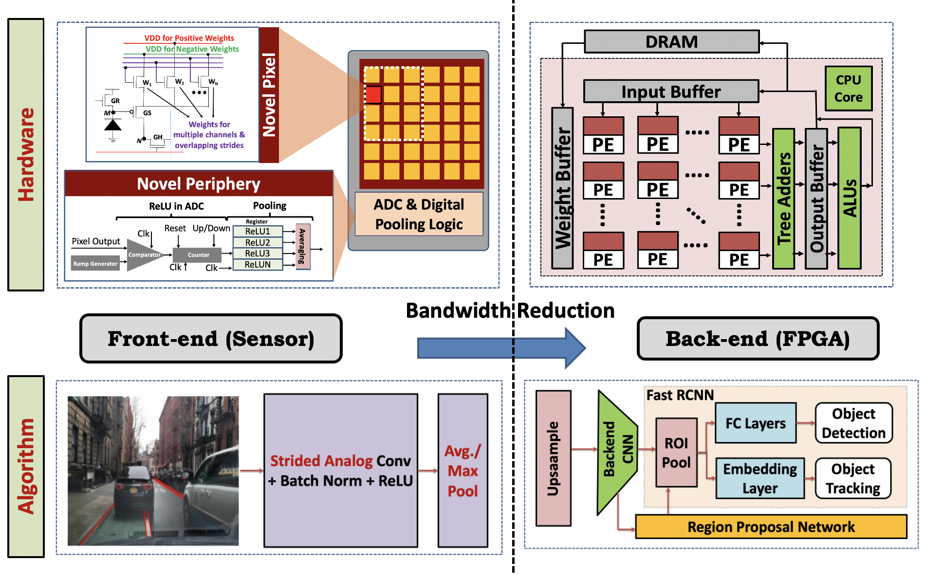
To the best of our knowledge, this work is the first to show the feasibility of scaling analog processing-in-pixel paradigms, specifically the P2M paradigm, to large-scale complex computer vision applications like real-time multi-object detection and tracking. As illustrated in Fig. 1, our approach termed P2M-DeTrack enables the support for non-overlapping strides that improves task accuracy and max/average pooling that jointly yields up to bandwidth reduction between the image sensor and back-end processing unit. We show how parallelism within P2M-DeTrack mitigates the large latencies induced by non-overlapping strides, thereby meeting the high frames per second (FPS) needed for real-time detection and tracking. More specifically, we present and evaluate P2M-compatible faster R-CNN-based detection [25] and tracking [23] models obtained via extensive algorithm-hardware co-design. We choose BDD100K [32] to validate our approach because it incorporates geographic, environmental, and weather diversity as well as intentional occlusions, and is the most comprehensive open-source dataset for large-scale object detection and tracking geared towards autonomous driving. Our resulting models obtain significant reductions in communication bandwidth, total latency, and energy consumption with negligible drop in detection and tracking accuracies.
II Preliminaries
II-A P2M: Processing-in-Pixel-in-Memory Paradigm
The P2M framework proposed in [7] implements multi-bit, multi-channel, non-overlapping strided convolution using memory (weight)-embedded pixels. The weights are represented by the transistor widths [31], which modulates the pixel outputs, and the BN and ReLU operations are implemented in the periphery of the pixel array using available on-chip column parallel ADCs in CMOS image sensors. Although the width-encoded weights are fixed during manufacturing, this lack of programmability may be more than an acceptable penalty because the first few layers of any computer vision (CV) model extract high level features that can be common across various visual tasks. Moreover, we can also reconfigure the weights by mapping them to emerging resistive non-volatile memory elements embedded within individual pixels [7]. P2M leverages the existing on-chip correlated double sampling (CDS) circuit in commercial cameras to accumulate both negative and positive weights that are needed to train accurate CV models. Note that the CDS circuit also helps implement the subsequent ReLU operation. Interested readers are referred to [7] for more details of the P2M circuit implementation.
II-B Object Detection & Tracking
QDTrack is a tracking by detection method [23] that uses a two stage detector such as faster R-CNN [25] to associate region proposals in temporal neighborhood using contrastive loss. This helps to associate identical objects in the same representation space while pushing dissimilar objects apart. QDTrack creates a per frame representation for each object detected which is then used in nearest neighbor search to do association between frames. In this work, we adopt the state-of-the-art (SOTA) QDTrack method with the faster R-CNN architecture for detection to validate our approach.
III Proposed Methodology
In this section, we first present our algorithm-hardware co-design framework that enables the support for non-overlapping strides and pooling layers which improves task accuracy. Our framework also enables real-time detection and tracking by exploiting column parallel ADCs for improved analog processing throughput. Lastly, we analytically derive the bandwidth reduction (which leads to energy and latency savings) obtained by P2M-DeTrack.
III-A Algorithm-Hardware Co-Design
Strided Convolution: In order to implement the strided convolution needed by object detection models, we propose to embed each pixel with different sets of weight transistors, depending on the value of the stride. In particular, as illustrated in Eq. 1, the maximum number of required transistors () per pixel is calculated as
| (1) |
where , , and are the kernel size, stride, and the number of output channels of the in-pixel layer. Notice that a lower stride value improves detection and tracking accuracy but incurs more transistors and higher required data transmission bandwidth between the sensor and back-end processing unit.
Pooling: The pooling layer in a CNN backbone reduces both the spatial dimensions of a feature map. In order to increase bandwidth reduction, we propose to implement the first pooling layer, following the convolutional, BN, and ReLU layers, inside the P2M chip. To achieve this, we buffer the outputs of the counter (of a single-slope ADC) used to implement the ReLU [7], and perform an ‘average’ or ‘max’ operation by digital logic in the periphery of the pixel array, as illustrated in Fig. 1. Consequently, we can map all the computational aspects of modern CNN layers inside the sensor chip through P2M analog computing.
P2M-DeTrack Parallelism: Enabling P2M-DeTrack computations inside the pixel array opens up a new opportunity to improve in-pixel parallelism for a given channel. Consider Fig. 2 that shows a pixel array of size 55 and 22 kernel with a stride of 1. Operating on Row-1 and Row-2 across two cycles (Fig. 2(a) and Fig. 2(b)), all the output activations corresponding to the horizontal striding can be generated. Note, for each kernel one ADC in the periphery, represented with same color coding as the corresponding kernel, is activated to convert the analog convolution operation into digital activations. More generally, this implies for each kernel of size only one among -ADCs is being utilized, leaving (-1) ADCs idle (not used) per columns. Fig. 2 presents a method to exploit such idle ADCs to improve processing parallelism. Specifically, for each column, kernels can be activated, simultaneously. ADCs on columns would be used to convert the analog convolution output to digital activation. Assuming a stride of , clock cycles are required to process each row, where denotes the ceiling function. On the other hand, using ADCs in parallel for each kernel, implies that only cycles are required to process each column, where is the height of the output activation map (which equals the height of the input activation map divided by ). Consequently, the number of clock cycles required to yield the complete digital output activation map for a given channel is
| (2) |
In this way, P2M-DeTrack enables row and column parallelism, transforming the pixel array into multiple analog parallel processing blocks.
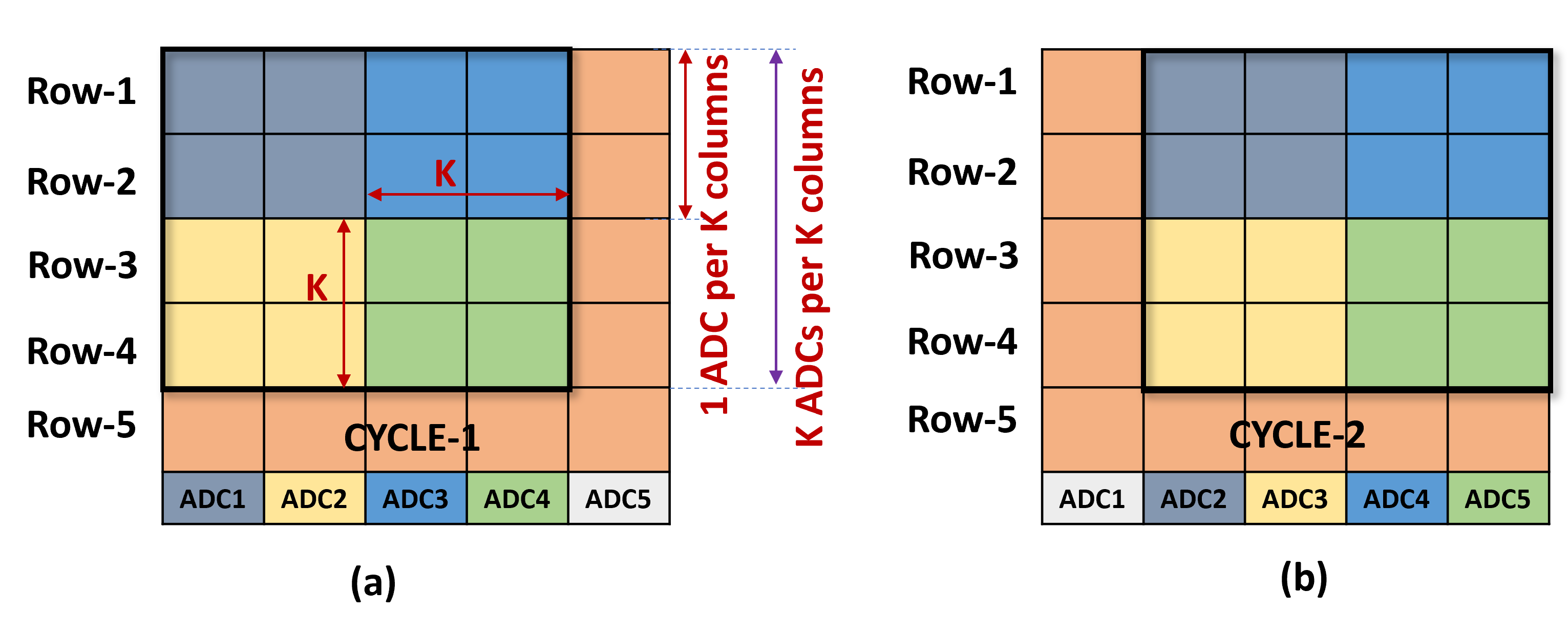
Discussion: The parallelism in P2M-DeTrack within a channel is limited by the amount of overlapping of the kernels. More precisely, it takes cycles to execute each pixel row. In addition, the different channels must be executed on the pixel array sequentially. Moreover, the number of required weight transistors per pixel is dependent on the kernel size, stride, and number of channels which is limited by area and technology constraints [7]. These constraints motivate a circuit-algorithm co-design that minimizes the number of channels and maximizes the stride subject to FPS requirements and achieving close to state-of-the-art (SOTA) accuracy. Finally, to achieve these accuracy goals, we must consider the non-linearities of the analog circuitry in the training process [7]. In particular, we focus on maximizing the mean average precision (mAP) corresponding to an intersection of union (IoU) averaged uniformly from 0.5 to 0.95 with a step size of 0.05, and mean identification F1 score (IDF1) [23] for object detection and tracking, respectively.
III-B Bandwidth Reduction
To quantify the bandwidth reduction (BR) by the P2M-implemented layers, let the number of elements in the RGB input image be and in the output activation map after the pooling layer be . Then, can be estimated as
| (3) |
Here, the factor denotes the demosaicing operation [1], which converts the Bayer’s pattern of RGGB pixels to RGB pixels by either ignoring the additional green pixel or designing the circuit to effectively take the average of the photo-diode currents coming from the green pixels. The factor denotes the ratio of the bit-precision between the image pixels captured by the sensor (pixels typically have a bit-depth of [22]) and the quantized output of the first convolutional layer denoted as . Let us now substitute
into Eq. 3, where denotes the spatial dimension of the input image and denotes the number of output channels of the first convolutional layer. While , , denote the kernel size, padding and stride of the in-pixel convolutional layer, respectively, similar notations with the prime superscript ′ denote the same hyperparameters of the pooling layer. We report the BR obtained by some of the these hyperparameter combinations (selected based on the design space exploration approach discussed above) in Table I.
| Convolutional | Pooling | ReLU output | Transistors/ | Bandwidth |
| stride () | stride () | bit-width () | pixel () | Reduction (BR) |
| 2 | 2 | 8 | 256 | 6 |
| 4 | 2 | 8 | 64 | 24 |
| 6 | - | 8 | 64 | 13.5 |
IV Simulation Results
In this section, we first introduce the implementation details and present our detection and tracking results on the BDD100K dataset. We then provide the energy consumption and FPS improvements obtained by our approach.
IV-A Experimental Setup
We evaluate P2M-DeTrack on BDD100K detection and tracking datasets with 12 and 10 object categories, respectively. While the detection set includes 70,000 images for training, and 10,000 images for validation, the tracking dataset includes 1,400 videos (278K images) for training and 200 videos (40K images). All these images have a resolution of 1.06M Pixel. Note that we report results on the validation dataset. The images in the tracking set are annotated per FPS with a FPS video frame rate111We observe that dropping every other frame does not lead to any degradation in the tracking IDF1 score for the BDD100K dataset.. We use the 2x training schedule consisting of 24 epochs and the 1x training schedule consisting of 12 epochs for our object detection and tracking experiments respectively. While our detection models are trained on 2 GPUs, each with a batch size of 2, our tracking models use 4 GPUs, each with a batch size 10. For both these experiments, we use the SGD optimizer with an initial learning rate of 0.0025.
For a fair comparison, all results are produced using the MMDetection framework [4] and the standard COCO-style evaluation protocol. In addition, we use ImageNet-pretrained ResNet-50 as the backbone to all our models and fine-tune the learning rate schedules of each model to obtain the best detection mAP. All our proposed models process the first four layers (convolutional+BN+ReLU+pooling) inside the sensors and the remaining layers in the back-end, while the baseline models process the entire neural network in the back-end.
| Model | Pool | mAP (%) | mAP (%) | mAP (%) | ||
| type | (IoU=0.5) | (IoU=0.75) | (IoU=0.5-0.95) | |||
| Faster R-CNN [25] | 2 | Max | 2 | 57.5 | 33.2 | 33.7 |
| P2M-DeTrack | 2 | Max | 2 | 56.5 | 32.9 | 33.2 |
| P2M-DeTrack | 6 | - | - | 55.5 | 31.7 | 32.3 |
| P2M-DeTrack | 4 | Avg | 2 | 53.5 | 30.3 | 31.1 |
IV-B Bandwidth vs. number of transistors
As summarized in Table I, we evaluated several model configurations that explore the trade-off between the bandwidth reduction and the number of weight transistors per pixel. With a kernel size of 7, a stride of 4 in the convolutional layer and a stride of 2 in pooling layer leads to a BR of 24, but requires a maximum of 64 weight transistors per pixel. A convolutional stride of 6 with no pooling leads to a BR of 13.5, also with a maximum of 64 weight transistors per pixel222Note that fewer pixels need 64 weight transistors for a stride of 6 than for a stride of 4.. Note, using chip stacking in which weight transistors are integrated vertically on a stacked chip through metal-to-metal fusion bonding [10] or through-silicon-vias (TSVs) [21], minimal to no increase in pixel area is expected because of the dense metal-pitch (MP) and contacted poly-pitch (CPP) [11] of advanced technology nodes and the relatively large sizes of underlying pixel arrays.
In addition, to improve the accuracy of downsampled output feature maps of the sensor, the feature maps are upsampled in the back-end processing unit, as shown in Fig. 1. In particular, the spatial dimension at the input of the back-end is chosen to be no less than of the image dimension. In general, the data generated from sensor has to be transferred through costly wired or wireless channels, which could form the key energy bottleneck for the overall system, particularly if the physical distance between the front- and back-end is large.
IV-C Detection Results
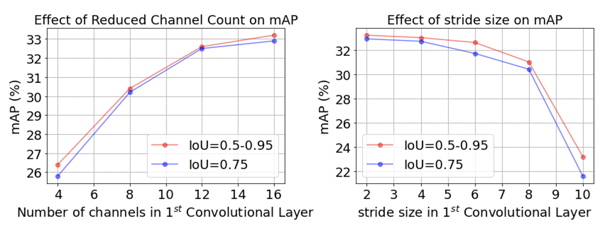
We developed multiple detection and tracking models with different strides in the convolutional and pooling layers (see Table I) as shown in Table II. The evaluated models in Table I yield mAPs for IoU=0.5:0.95 within 1% of the baseline model, as detailed in Table II. We also ablate over the number of channels and strides in Fig. 3 to understand the limits of bandwidth reduction. The figure shows that the mAP drops beyond 1% as we decrease the number of channels below 16. A similar significant accuracy drop is observed for strides above 6. Note that we also increase the kernel size (i.e., make the kernel size equal to stride) to support strides of 8 and 12.
IV-D Tracking Results
The detailed breakdown of our tracking results on the BDD100K multi-object tracking (MOT) validation set are shown in Table III. Our P2M-DeTrack models achieve 49.7% mIDF1 (stride 2, pool 2) and 49.1% mIDF1 (stride 6, pool 2, followed by upsampling), both of which are comparable to the SOTA 50.8% mIDF1 obtained by QDTrack [23].
| Model | mMOTA | mIDF1 | MOTA | IDF1 | FN | FP | ID Sw. | mAP | ||
|---|---|---|---|---|---|---|---|---|---|---|
| QDTrack [23] | - | - | 36.6 | 50.8 | 63.5 | 71.5 | 108614 | 46621 | 6262 | 32.6 |
| P2M-DeTrack | 2 | 2 | 34.0 | 49.7 | 62.4 | 70.7 | 119256 | 41466 | 5964 | 30.8 |
| P2M-DeTrack | 6 | - | 34.2 | 49.1 | 61.8 | 70.3 | 122691 | 40480 | 5999 | 30.3 |
IV-E Reduction in Energy Consumption
As described in [7], the total energy consumption for both P2M-DeTrack and conventional baseline models can be partitioned into three major components, sensor (), sensor-to-SoC communication (), and SoC energy () as captured in Eq. 4. Note that is the sum of the pixel array energy333The pixel array energy is equal to the image read-out energy for the baseline models and in-pixel convolution energy for custom models. and the ADC energy; both are obtained from circuit simulations using commercial Globalfoundries 22nm FD-SOI technology node. is computed from as shown in Eq. (4), and its value shown in Table IV is obtained from [15]. On the other hand, in primarily dominated by multiply-and-add (MAdd) energy of the models used for detection ().
| (4) |
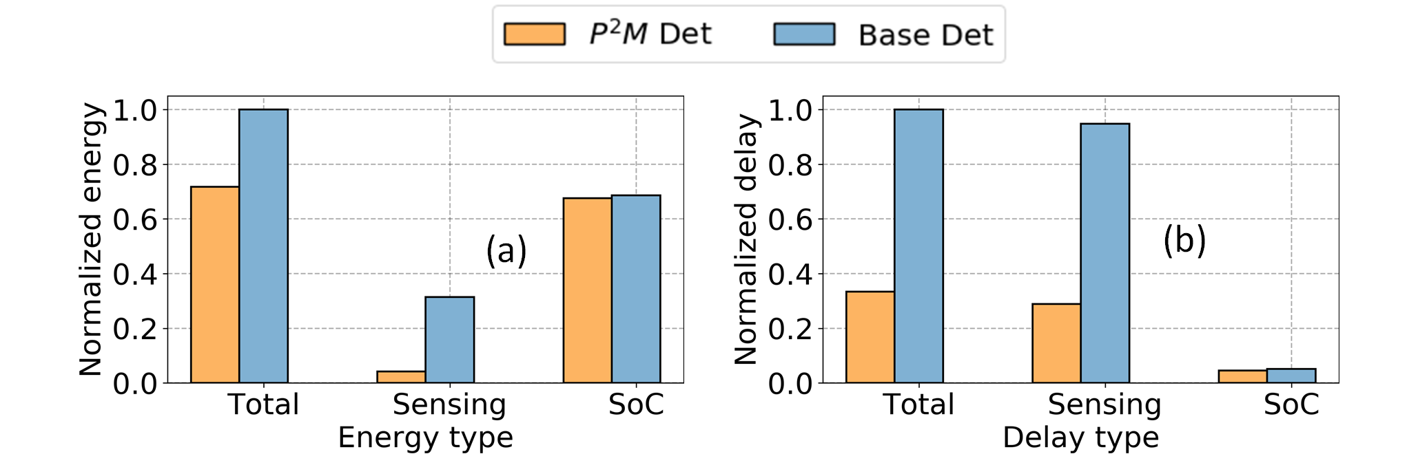
Fig. 4 shows the normalized energy comparison between P2M-DeTrack and baseline detection models. In particular, the in-pixel architecture is estimated to reduce the sensing energy by up to with a total energy improvement of . Note, in Eq. 4 and corresponds to the total number of pixels needed to be processed in-pixel and total MAC operations [16] for the back-end model, respectively. We note that the dominating back-end can be often over-parameterized and thus various off-the-shelf model compression [17, 24] can be deployed to further reduce the back-end computation cost. This, in turn, can further reduce the total energy.
IV-F Reduction in Delay
The delay associated with the detection pipeline can be partitioned in to four components, sensing delay (), ADC delay (), communication delay (), and backend delay () as shown below
| (5) |
We use the per-pixel communication delay from [9] to estimate the delay required to send the output activation maps from sensor to SoC (). While is primarily governed by the sensor read delay, is associated with the total number of ADC clock cycles required to generate the first layer output activation map, dictated by our P2M-DeTrack parallelism approach discussed in Section III-A. Note that both of these values are computed from our circuit simulations.
| Notation | Description | Value |
|---|---|---|
| Sensing energy/#pixel | 148 pJ (P2M) | |
| 312 pJ (baseline) | ||
| ADC energy/#pixel | 41.9 pJ (P2M) | |
| 86.14 pJ (baseline) | ||
| SoC comm. energy/#pixel | 900 pJ | |
| Madds energy in technology | 1.568 pJ |
was computed by the Xilinx FINN-based [29] FPGA simulation framework targetting the Xilinx Alveo U250 platform, which was modified to include the QSFP+ high-speed transceiver for streaming purposes. Our framework utilizes High-Level Synthesis (HLS) to translate the developed PyTorch model into a synthesizable RTL to generate a bitstream for the target Alveo U250 device. The HLS flow evaluates the network layers, splits each layer into submodules, and applies transformations to aid in the HLS conversion process. These transforms are intended to optimize the HLS process by enabling FPGA-friendly quantization, pipeline the FIFO insertions, and implementations for efficient memory (BRAM, URAM and LUTRAM) and processing (DSP) for all layers. The resulting model is stitched back together in RTL submodules and run through synthesis, place-and-route, leading to the final bitstream generation. This process allows for refining individual modules and stages with HLS and analyzing latency and resource utilization for the system bottlenecks.
The resulting inference latency through the system implementing only the CNN backbone is 15.5 ms. The resource utilization is 60% LUTs, 30% Flip-Flops, 13% DSPs, 60% BRAMs, 10% LUTRAMs and 2% URAMs. The power utilization is 70W based on default switching models as reported by the Xilinx Vivido tools. Augmenting the baseline ResNet-50 model to our proposed custom network with the first convolutional, BN, ReLU, and pooling layers removed, results in a improvement in latency, down to ms. As shown in Fig. 4, the total delay improvement for in-pixel architecture is estimated to be up to . In particular, the proposed P2M-DeTrack model can yield an improved FPS compared to the baseline’s FPS, which may be acceptable for real-time detection and tracking in an autonomous driving scenario. Note that the FPS can be further improved by using faster pixels or by designing and leveraging more than one ADC per column. For example, using 2 ADCs per column can double the FPS at the cost of only modest increase in area.
V Conclusions and Discussions
This work proposes P2M-DeTrack, a processing-in-pixel-in-memory-based algorithm-hardware co-design framework that can reduce the EDP cost of a complex object detection and tracking pipeline by up to ( reduction in latency for a reduction in energy) compared to existing in-sensor processing approaches. Our hardware modifications can be readily integrated into the foundry-manufacturable CMOS image sensor platforms, and our hardware-inspired algorithmic modifications are shown to yield negligible performance drop in multi-object detection and tracking. To the best of our knowledge, we are the first to incorporate all the computational aspects of modern CNN layers inside CMOS image pixels, and show the feasibility of in-pixel computing for complex vision tasks on high-resolution (1Mpixel) datasets, including real-time multi-object detection and tracking. Our future work includes pruning and quantizing the faster R-CNN back-end to further optimize the system FPS and energy consumption. We also plan to incorporate the region proposal network of the faster R-CNN architecture in our FPGA simulation and analytical framework, which would further improve our energy and delay estimation models.
It is important to note that the energy metric presented in this work is based on the assumption that the front-end and back-end chips are closely located on the same printed-circuit board [15]. In general, the front-end and back-end sensors could be separated by large distances, necessitating long energy-expensive wired or wireless data transfer (which is common for the case of sensor-fusion and swarm intelligence applications). In such cases the overall energy improvement would approach the bandwidth reduction (up to 24) obtained from the proposed P2M-DeTrack scheme.
References
- [1] Demosaicing for Quad-Bayer Sensors. http://image-sensors-world.blogspot.com/2021/04/demosaicing-for-quad-bayer-sensors.html, 2021.
- [2] Shaahin Angizi et al. PISA: A binary-weight processing-in-sensor accelerator for edge image processing. arXiv preprint arXiv:2202.09035, 2022.
- [3] Laurie Bose et al. Fully embedding fast convolutional networks on pixel processor arrays. In Computer Vision - ECCV 2020 - 16th European Conference, Glasgow, UK, August 23-28, 2020, Proceedings, Part XXIX, volume 12374, pages 488–503. Springer, 2020.
- [4] Kai Chen et al. MMDetection: Open MMLab detection toolbox and benchmark. arXiv preprint arXiv:1906.07155, 2019.
- [5] Zhe Chen et al. Processing near sensor architecture in mixed-signal domain with cmos image sensor of convolutional-kernel-readout method. IEEE Transactions on Circuits and Systems I: Regular Papers, 67(2):389–400, 2020.
- [6] Gourav Datta et al. ACE-SNN: Algorithm-hardware co-design of energy-efficient & low-latency deep spiking neural networks for 3d image recognition. Frontiers in neuroscience, page 400.
- [7] Gourav Datta et al. P2M: A processing-in-pixel-in-memory paradigm for resource-constrained tinyml applications. arXiv preprint arXiv:2203.04737, 2022.
- [8] Gourav Datta et al. Toward efficient hyperspectral image processing inside camera pixels. arXiv preprint arXiv:2203.05696, 2022.
- [9] Yiming Gan et al. Low-latency proactive continuous vision. Proceedings of the ACM International Conference on Parallel Architectures and Compilation Techniques, 2020.
- [10] Guilian Gao et al. Chip to wafer hybrid bonding with Cu interconnect: High volume manufacturing process compatibility study. In 2019 International Wafer Level Packaging Conference (IWLPC), pages 1–9.
- [11] M Gupta et al. High-density SOT-MRAM technology and design specifications for the embedded domain at 5nm node. In 2020 IEEE International Electron Devices Meeting (IEDM), pages 24–5, 2020.
- [12] Akhilesh Jaiswal and Ajey Jacob. Integrated pixel and three-terminal non-volatile memory cell and an array of cells for deep in-sensor, in-memory computing, July 20 2021. US Patent 11,069,402.
- [13] Akhilesh Jaiswal and Ajey Jacob. Integrated pixel and two-terminal non-volatile memory cell and an array of cells for deep in-sensor, in-memory computing, Dec. 7 2021. US Patent 11,195,580.
- [14] Kyoung-Don Kang et al. Real-time information derivation from big sensor data via edge computing. Big Data and Cognitive Computing, 1:5, 10 2017.
- [15] Venkatesh Kodukula et al. Dynamic temperature management of near-sensor processing for energy-efficient high-fidelity imaging. Sensors, 1(3), 2021.
- [16] Souvik Kundu et al. Pre-defined sparsity for low-complexity convolutional neural networks. IEEE Transactions on Computers, 69(7):1045–1058, 2020.
- [17] Souvik Kundu et al. DNR: A tunable robust pruning framework through dynamic network rewiring of dnns. In Proceedings of the 26th Asia and South Pacific Design Automation Conference, pages 344–350, 2021.
- [18] Weitao Li et al. Timely: Pushing data movements and interfaces in pim accelerators towards local and in time domain. In Proceedings of the ACM/IEEE 47th Annual International Symposium on Computer Architecture, ISCA’20, page 832–845, 2020.
- [19] Tianrui Ma et al. An analog-memoryless near sensor computing architecture for always-on intelligent perception applications. In 2019 IEEE International Conference on Integrated Circuits, Technologies and Applications (ICTA), volume 1, pages 150–155, 2019.
- [20] Lukas Mennel et al. Ultrafast machine vision with 2D material neural network image sensors. Nature, 579:62–66, 2020.
- [21] Makoto Motoyoshi. Through-silicon via (TSV). Proceedings of the IEEE, 97(1):43–48, 2009.
- [22] ON Semiconductor. CMOS Image Sensor, 1.2 MP, Global Shutter, 3 220. Rev. 10.
- [23] Jiangmiao Pang et al. Quasi-dense similarity learning for multiple object tracking. In 2021 IEEE/CVF Conference on Computer Vision and Pattern Recognition (CVPR), volume 1, pages 164–173, 2021.
- [24] Ao Ren et al. ADMM-NN: an algorithm-hardware co-design framework of DNNs using alternating direction methods of multipliers. In Proceedings of the Twenty-Fourth International Conference on Architectural Support for Programming Languages and Operating Systems, pages 925–938, 2019.
- [25] Shaoqing Ren et al. Faster R-CNN: Towards real-time object detection with region proposal networks. arXiv preprint arXiv:1506.01497, 2015.
- [26] Oindrila Saha et al. RNNPool: Efficient non-linear pooling for RAM constrained inference. In H. Larochelle, M. Ranzato, R. Hadsell, M. F. Balcan, and H. Lin, editors, Advances in Neural Information Processing Systems, volume 33, pages 20473–20484, 2020.
- [27] Ruibing Song et al. A reconfigurable convolution-in-pixel cmos image sensor architecture. arXiv preprint arXiv:2101.03308, 2021.
- [28] Badri Narayan Subudhi et al. Big data analytics for video surveillance. Multimedia Tools Appl., 78(18):26129–26162, sep 2019.
- [29] Yaman Umuroglu et al. FINN: A framework for fast, scalable binarized neural network inference. In Proceedings of the 2017 ACM/SIGDA International Symposium on Field-Programmable Gate Arrays, FPGA ’17, pages 65–74. ACM, 2017.
- [30] Jorge Vargas et al. An overview of autonomous vehicles sensors and their vulnerability to weather conditions. Sensors, 21(16), 2021.
- [31] H.-S. Philip Wong et al. Metal–oxide RRAM. Proceedings of the IEEE, 100(6):1951–1970, 2012.
- [32] Fisher Yu et al. BDD100K: A diverse driving dataset for heterogeneous multitask learning. arXiv preprint arXiv:1805.04687, 2018.