Plasmonics enabled atomically thin linearly polarized emitter at room temperature
Bidisha Roy1,2, Mäx Blauth1, Siddharth Dhomkar3, Michael Kaniber1, Vinod M. Menon4,5 and Jonathan. J. Finley1
1
Walter Schottky Institute, Technical University of Munich
Am Coulombwall 4, 87548 Garching bei Munich, Germany
2
Centre for Nano Science and Engineering
Indian Institute of Science, Mathikere, Bengaluru 560012, India
3Centre for Nanotechnology, University College London
London WC1H OAH, United Kingdom
4Department of Physics, City College of New York
City University of New York, 160 Convent Avenue, New York 10031, USA
5Department of Physics, CUNY Graduate Center
365 Fifth Avenue, New York 10016, USA
Two-dimensional transition metal di-chalcogenide semiconductors provide unique possibilities to investigate strongly confined excitonic physics and a plasmonic platform integrable to such materials constitutes a hybrid system that can be of interest to enable manipulation of their cumulative optical properties. Here we report tuning of excitonic emission from monolayer WSe2, mechanically exfoliated on top of a periodic two dimensional plasmonic array of elliptical gold (Au) nanodiscs. By exploiting the polarization-dependent nature of plasmonic resonance of the nano plasmonic array (NPA), the photoluminescence (PL) emission from the overlaid monolayer WSe2 could be significantly manipulated. PL is preferentially enhanced at the NPA covered regions of the flake when excited closer to the plasmonic resonant frequencies and previously unpolarized WSe2 PL emission gained 20 up to 40 % degree of linear polarization at room temperature. Obtaining significant spectral overlap between the PL spectrum of WSe2 and the polarization tunable plasmonic resonance of the NPA plays a crucial role in this observation. The results demonstrate active tunability of optical emission from WSe2 by using an otherwise passive plasmonic environment and opens the possibility of achieving atomically thin linearly polarized emitters at room temperature. In addition to fundamentally interesting physics of such interactions this can be highly desirable for ultrathin orientation sensitive opto-electronic device related applications.
KEYWORDS: plasmonics, 2D TMDC, WSe2, photoluminescence, nanoplasmonic array, polarization.
1 Introduction
Investigating optical processes in optically active low dimensional materials in modified photonic environments remain of great interest and importance in the study of light matter interactions. Owing to their remarkable optical, electronic and quantum properties, the field of atomically thin two-dimensional (2-D) transition metal dichalcogenides (TMDCs) has been looked upon for bringing a new paradigm in materials physics of semiconductors showing surge of promising applications in optoelectronics, photonics and valleytronics (ref.[1, 2, 3, 4] and references therein). From few layers to monolayer limit these materials become direct band gap semiconductors [5, 6]; reduced dimensionality, strong excitonic binding energies ( few 100 meV), preferential crystal symmetries, unique combination of spin and valley degrees of freedom, well demonstrated strong light matter coupling [7, 8, 9] etc. make them relevant for both fundamental and applied studies. Plasmonics on the other hand, offers to be an easily integrable platform to these materials providing alterable photonic environment to explore and achieve interesting effects such as enhanced quantum efficiency [10], strong plasmon-exciton coupling [11, 12, 13], electrical tunability of such coupling [14, 15], deep subwavelength guiding of light [16], second harmonic generation covering the entire visible range [17], etc. In this context, investigating integrated 2D- TMDCs – plasmonic hybrid system remain interesting for fundamental studies as well as is critical in realizing novel optical devices with applications such as integrated on-chip quantum nanophotonics, improved light sources, detectors and sensors etc.
In this paper, we investigated a system that consists of a monolayer WSe2 flake, which is intentionally placed on top of a 2D periodic Nano plasmonic array (NPA) with elliptical gold nano discs. NPAs are ideal for easy integration and possibility of larger area interaction with the 2D material. Additionally, the nature of inter particle coupling of the localized plasmonic dipoles can be exploited from near-field to intermediate to far-field by adjusting the periodicity of plasmonic elements in the NPAs. This may offer an effective way to control the interaction between the excitonic response and the near or far field dipolar-coupled localized plasmonic resonances. In the last years WSe2 has gained much significance lately amongst the other members of the 2D TMDC family, due to its unique valley polarization and coherence properties [18, 19, 20], optically dark ground excitonic state [21, 22, 23], and the reports of observing single quantum emitters within its defect states [24, 25, 26]. Here, however, we report an interesting set of observations as seen from the room temperature PL emission of WSe2 in the absence and presence of a simplistically tunable plasmonic environment. Using polarization dependent reflection spectroscopy, 2D fluorescence mapping, and polarization dependent photoluminescence spectroscopy, we study this influence and achieve an external control over the emission polarization of WSe2 PL by using the polarization tunability of the plasmonic resonance of the NPA pertaining to the geometry. This paves the path to realizable atomically thin linearly polarized emitters at room temperature.
2 Results and Discussions
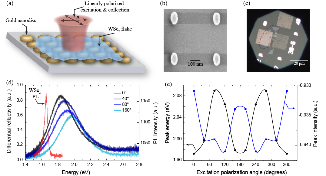
Elliptical gold (Au) discs (30 nm high, short and long axes radii ranging from 20 to 60 nm) arranged in two dimensional periodic square array lattices (periodicity ranging from 580 to 800 nm) were fabricated using e-beam lithography on 150 µm thick glass substrate. After careful investigation of the fabricated NPAs, monolayer flake of WSe2 was mechanically exfoliated on to a PDMS strip and transferred on top of the NPA of interest comprised of ellipses with 50 nm 60 nm short and long axes radii, respectively, arranged in a 20 µm 20 µm 2D periodic array with the periodicity of 600 nm. A schematic of the sample of interest is shown in Fig.1 (a). Details on optimization, fabrication of the nanoplasmonic array and exfoliation of WSe2 flake can be found in the supplementary information. Fig. 1(b) and (c) respectively show a close up SEM image of a suggestive NPA of elliptical discs and an optical microscopic image of the transferred WSe2 flake over the region of interest (highlighted by the red dashed line for eye guidance).
For a single metal nanoparticle the plasmonic resonance strongly depends on details of the the geometric shape and material properties of the particle as well as the surrounding medium. For an ensemble of particles the individual plasmon resonance is additionally influenced by the electromagnetic particle interaction. Depending upon the inter-particle separation between the plasmonic particles, if exceeding the near field coupling distances, typically a far field interaction is mediated by the scattered light fields which are dipolar in nature. For a two dimensional square grating of metal nanoparticles interacting only in the far field regime, particularly strong dipolar interaction arises when the light field corresponding to a particular grating order change from evanescent to radiative in character [27, 28]. In this work as the 2D NPA is comprised of elliptical gold nano discs with 600 nm separation, the overall plasmonic resonance is a scalar cumulative effect arising from the strong far-field-coupled dipolar interactions between the individual localized plasmonic scatterers. Typical plasmonic response to broad band optical excitation of the NPA is shown in Fig. 1(d). The plasmon resonance is revealed through the measurement of differential reflectivity which is the relative change of reflectivity w.r.t that of the substrate. A broadband light source was used for the reflection spectroscopy measurements. After initial adjustment of the excitation power and the polarization, the beam is passed through a beamsplitter and is focused to the sample surface by an achromatic microscope objective (NA = 0.9). To take in account the cumulative scattering from the array a large focused excitation spot ( 12 micron diameter) was used by modifying the optics. The reflected light from the sample surface is collected by the same objective, passed through the beamsplitter and guided to a spectrometer where it is spectrally analyzed. Fig 1 (d) shows that the broad plasmonic resonance from the array is dependent on the excitation polarization w.r.t the geometrical axis of the ellipses. In Fig 1(e) the expected behavior of the plasmon resonance as a function of the excitation polarization angle (w.r.t the geometrical axis of the ellipse) is shown as obtained from simulations. It is clear that the plasmon resonance peak intensity and energy go through a periodic oscillation due to the symmetry of the elliptical discs. More details on the simulation set up and results can be found in supplementary information. This dependence of the plasmonic resonance on the excitation polarization due to the geometry of the elliptical discs, is one of the key aspects of this work. Figure 1(d) also shows the room temperature PL from bare WSe2 monolayer (PL peak at 1.65 eV). It has been reported that the main exciton emission peak of WSe2 PL at room temperature is from the bound ‘neutral’ exciton with high binding energy;(where the electrons and holes are tightly bound together and are relatively more stable to endure the thermal fluctuations compared to other conventional semiconductors). The PL is overlaid to the plasmonic reflection spectra showing significant spectral overlap between the plasmonic resonance and the excitonic PL at room temperature.
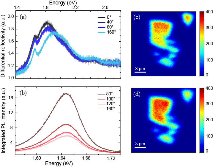
Differential reflectivity from the WSe2 covered NPA is shown in Fig 2 (a) revealing the appearance of WSe2 absorption edge at the lower energy side in addition to the plasmonic resonance (as seen from the bare plasmonic array). Fig. 2(b) shows the integrated PL intensity from the WSe2 flaked array excited at the plasmonic resonance (with a 633 nm red laser) for varied angles of linear polarized excitation. This demonstrates that while exciting the WSe2 at the peak of plasmonic resonance a significant tunability of the PL from the overlaying WSe2 flake could be achieved by simply changing the linear polarization of the excitation beam.
To further investigate into the nature of this interaction, two different excitation sources – a 533 nm green laser (off-resonant w.r.t the plasmon resonance energy) and a 633 nm red laser (resonant with plasmon resonance energy) – were used to obtain a spatial fluorescence map of the WSe2 flake on and off the plasmonic array (we note that both of the excitation are above band gap for WSe2 neutral excitonic transition energy). Fig. 2 (c) and (d) show the fluorescence 2D map with Green and red excitation respectively. The triangular region in upper right side corner is the bare WSe2 flake while the bigger region at the center is the flake covering the NPA. The map clearly shows preferential enhancement of the luminescence intensity from the WSe2 flake overlaying the NPA site as compared to that of the bare flake site only for resonant plasmon excitation (in fig. 2(d)) while for the off plasmonic excitation such an effect is absent (fig. 2(c). We note that this preferential enhancement is not due to any selective increase in effective absorption cross section of WSe2 and hence this preferential enhancement as observed predominantly for the plasmonic resonant excitation is a consequence of the plasmonic environment.

In order to gain further insight on the influence of plasmonic resonant excitation on PL of WSe2, detailed investigations on the peak intensity and peak energy were performed. Fig.3 shows the peak intensity and peak energy of plasmonic resonance and WSe2 PL (for 633 nm i.e. near plasmonic resonant excitation) plotted in a 2D map as a function of the excitation polarization angle ( on the x-axis) and collection polarization angles ( on the y-axis). Fig. 3 (a) and (b) demonstrate the geometry dependent scattering response (from differential reflectivity measurement) and polarization profile of the plasmonic resonance from the bare NPA as a function of the excitation and collection polarization angles. High degree of linear polarization is evident, as expected, from the elliptical geometry of the plasmonic particles. It is interesting, however, to note that this polarization property of the palsmonic array directly affects the excitonic PL emission of the WS covering the NPA as seen from Fig. 3 (c) and (d). The PL peak intensity and PL peak energy dependence on the excitation polarization angle and collection polarization angle, reveal emergence of significant degree of linear polarization in the emission PL of otherwise unpolarized WSe2 (as also seen in Fig. 3(g)and (h) for bare WSe2 flake where no deterministic linear polarization is observed). This gaining of polarization in the emission PL follows a specific correlation with the polarization response of the plasmonic array which indicates the response is predominantly plasmonics enabled in its nature. Figs. 3 (e) and (f) show the polar plot for two selected excitation polarization angles (45 and 90 degrees) clearly showing that PL of WSe2 overlaid upon the NPA is linearly polarized in the emission.
In general, no reports of valley coherence or linear polarized emission for WSe2 has been reported at the room temperature. Nonetheless we measure the degree of polarization upto 20-40% for WSe2 on the NPA. We further note that the polarization dependence of the PL does not exactly match with the symmetry of the plasmonic axes (which determines the polarization dependence of the plasmonic resonance itself) while it maintains a slightly shifted maxima-minima correlation with the same. This correlation is dependent on the amount of varying spectral overlap between the plasmonic resonance and excitonic PL spectra. The larger the spectral overlap, higher is the interaction between the plasmonic resonance and excitonic PL and higher is the degree of acquired linear polarization. Essentially, the overall effect can be seen as an additive and dynamic contribution from: 1) the “excitation channel” - where the local field enhancement (due to plasmonic scattering) can cause more efficient excitation of the WSe2 excitons especially at resonant plasmonic conditions and 2) the “emission channel” - where the interplay of the excitation polarization dependent variation of spectral overlap between the plasmonic resonance of NPA and PL of WSe2 facilitates a more dynamic and nontrivial interaction between the two species. We note that the geometric cross section of the metal filled NPA under WSe2 can be quantified in terms of a “Fill Factor” defined as the following ratio; Geometric Fill Factor = (Area with NPA)/(Area without NPA), which for our system is a merely 2%. For such a small factor, the contribution from local field enhancement should be insignificant to contribute significantly towards the excitation channel. Thus we conclude that the spectral overlap plays a more crucial role in the effects observed here. The tunability of the amount of spectral overlap between the plasmonic resonance and excitonic emission is the key to the tunability of the acquired non trivial polarization in the emission PL.
3 Conclusion
We report nanoplasmonic array enabled modification of PL emission from monolayer WSe2 integrated onto 2D array of elliptical gold nanodiscs. Using plasmonic resonant excitation the polarization studies revealed that significant degree of linear polarization was imparted to the otherwise unpolarized PL emission from WSe2 at room temperature. This opens up the possibility to obtain atomically thin linearly polarized emitters at room temperature by using array of simple geometrically appropriate plasmonic structures. This can be exploited further towards polarized light sources, flat panel display applications as well as novel alignment sensitivity based sensor applications.
References
- [1] Sheneve Z. Butler, Shawna M. Hollen, Linyou Cao, Yi Cui, Jay A. Gupta, Humberto R. Gutiérrez, Tony F. Heinz, Seung Sae Hong, Jiaxing Huang, Ariel F. Ismach, Ezekiel Johnston-Halperin, Masaru Kuno, Vladimir V. Plashnitsa, Richard D. Robinson, Rodney S. Ruoff, Sayeef Salahuddin, Jie Shan, Li Shi, Michael G. Spencer, Mauricio Terrones, Wolfgang Windl, and Joshua E. Goldberger. Progress, challenges, and opportunities in two-dimensional materials beyond graphene. ACS Nano, 7(4):2898–2926, 2013. PMID: 23464873.
- [2] Gang Wang, Alexey Chernikov, Mikhail M. Glazov, Tony F. Heinz, Xavier Marie, Thierry Amand, and Bernhard Urbaszek. Colloquium: Excitons in atomically thin transition metal dichalcogenides. Rev. Mod. Phys., 90:021001, Apr 2018.
- [3] Qing Hua Wang, Kourosh Kalantar-Zadeh, Andras Kis, Jonathan N Coleman, and Michael S Strano. Electronics and optoelectronics of two-dimensional transition metal dichalcogenides. Nature nanotechnology, 7(11):699, 2012.
- [4] John R Schaibley, Hongyi Yu, Genevieve Clark, Pasqual Rivera, Jason S Ross, Kyle L Seyler, Wang Yao, and Xiaodong Xu. Valleytronics in 2d materials. Nature Reviews Materials, 1(11):16055, 2016.
- [5] Kin Fai Mak, Changgu Lee, James Hone, Jie Shan, and Tony F. Heinz. Atomically thin : A new direct-gap semiconductor. Phys. Rev. Lett., 105:136805, 2010.
- [6] Andrea Splendiani, Liang Sun, Yuanbo Zhang, Tianshu Li, Jonghwan Kim, Chi-Yung Chim, Giulia Galli, and Feng Wang. Emerging photoluminescence in monolayer mos2. Nano letters, 10(4):1271–1275, 2010.
- [7] Xiaoze Liu, Tal Galfsky, Zheng Sun, Fengnian Xia, Erh-chen Lin, Yi-Hsien Lee, Stéphane Kéna-Cohen, and Vinod M Menon. Strong light–matter coupling in two-dimensional atomic crystals. Nature Photonics, 9(1):30, 2015.
- [8] S Dufferwiel, S Schwarz, F Withers, AAP Trichet, F Li, M Sich, O Del Pozo-Zamudio, C Clark, A Nalitov, DD Solnyshkov, et al. Exciton–polaritons in van der waals heterostructures embedded in tunable microcavities. Nature communications, 6:8579, 2015.
- [9] Christian Schneider, Mikhail M Glazov, Tobias Korn, Sven Höfling, and Bernhard Urbaszek. Two-dimensional semiconductors in the regime of strong light-matter coupling. Nature communications, 9(1):2695, 2018.
- [10] Bumsu Lee, Joohee Park, Gang Hee Han, Ho-Seok Ee, Carl H Naylor, Wenjing Liu, AT Charlie Johnson, and Ritesh Agarwal. Fano resonance and spectrally modified photoluminescence enhancement in monolayer mos2 integrated with plasmonic nanoantenna array. Nano letters, 15(5):3646–3653, 2015.
- [11] Wenjing Liu, Bumsu Lee, Carl H Naylor, Ho-Seok Ee, Joohee Park, AT Charlie Johnson, and Ritesh Agarwal. Strong exciton–plasmon coupling in mos2 coupled with plasmonic lattice. Nano letters, 16(2):1262–1269, 2016.
- [12] PAD Gonçalves, LP Bertelsen, Sanshui Xiao, and N Asger Mortensen. Plasmon-exciton polaritons in two-dimensional semiconductor/metal interfaces. Physical Review B, 97(4):041402, 2018.
- [13] Chelsea Carlson, Robert Salzwedel, Malte Selig, Andreas Knorr and Stephen Hughes. Strong coupling regime and hybrid quasinormal modes from a single plasmonic resonator coupled to a transition metal dichalcogenide monolayer. Physical Review B, 104(12):125424, 2021.
- [14] Bumsu Lee, Wenjing Liu, Carl H Naylor, Joohee Park, Stephanie C Malek, Jacob S Berger, AT Charlie Johnson, and Ritesh Agarwal. Electrical tuning of exciton–plasmon polariton coupling in monolayer mos2 integrated with plasmonic nanoantenna lattice. Nano letters, 17(7):4541–4547, 2017.
- [15] Biswanath Chakraborty, Jie Gu, Zheng Sun, Mandeep Khatoniar, Rezlind Bushati, Alexandra L Boehmke, Rian Koots, and Vinod M Menon. Control of strong light–matter interaction in monolayer ws2 through electric field gating. Nano letters, 18(10):6455–6460, 2018.
- [16] Mäx Blauth, M Juergensen, Gwenaëlle Vest, Oliver Hartwig, Maximilian Prechtl, John Cerne, Jonathan J Finley, and Michael Kaniber. Coupling single photons from discrete quantum emitters in wse2 to lithographically defined plasmonic slot waveguides. Nano letters, 18(11):6812–6819, 2018.
- [17] Yufeng Ding, Chengrong Wei, Huimin Su, Shuoyan Sun, Zhiyong Tang, Zhaona Wang, Guixin Li, Dahe Liu, Shangjr Gwo, Junfeng Dai, and Jinwei Shi. Second harmonic generation covering the entire visible range from a 2d material–plasmon hybrid metasurface. Advanced Optical Materials, 9(16):2100625, 2021.
- [18] G Wang, L Bouet, D Lagarde, M Vidal, A Balocchi, T Amand, X Marie, and B Urbaszek. Valley dynamics probed through charged and neutral exciton emission in monolayer wse 2. Physical Review B, 90(7):075413, 2014.
- [19] G Wang, MM Glazov, C Robert, T Amand, X Marie, and B Urbaszek. Double resonant raman scattering and valley coherence generation in monolayer wse 2. Physical review letters, 115(11):117401, 2015.
- [20] Kai Hao, Galan Moody, Fengcheng Wu, Chandriker Kavir Dass, Lixiang Xu, Chang-Hsiao Chen, Liuyang Sun, Ming-Yang Li, Lain-Jong Li, Allan H MacDonald, et al. Direct measurement of exciton valley coherence in monolayer wse 2. Nature Physics, 12(7):677, 2016.
- [21] Xiao-Xiao Zhang, Yumeng You, Shu Yang Frank Zhao, and Tony F Heinz. Experimental evidence for dark excitons in monolayer wse2. Physical review letters, 115(25):257403, 2015.
- [22] T Smoleński, M Goryca, M Koperski, C Faugeras, T Kazimierczuk, A Bogucki, K Nogajewski, P Kossacki, and M Potemski. Tuning valley polarization in a wse 2 monolayer with a tiny magnetic field. Physical Review X, 6(2):021024, 2016.
- [23] Mark Danovich, Viktor Zólyomi, and Vladimir I Fal’ko. Dark trions and biexcitons in ws 2 and wse 2 made bright by ee scattering. Scientific Reports, 7:45998, 2017.
- [24] Yu-Ming He, Genevieve Clark, John R Schaibley, Yu He, Ming-Cheng Chen, Yu-Jia Wei, Xing Ding, Qiang Zhang, Wang Yao, Xiaodong Xu, et al. Single quantum emitters in monolayer semiconductors. Nature nanotechnology, 10(6):497, 2015.
- [25] M Koperski, K Nogajewski, A Arora, V Cherkez, P Mallet, J-Y Veuillen, J Marcus, P Kossacki, and M Potemski. Single photon emitters in exfoliated wse 2 structures. Nature nanotechnology, 10(6):503, 2015.
- [26] Ajit Srivastava, Meinrad Sidler, Adrien V Allain, Dominik S Lembke, Andras Kis, and A Imamoğlu. Optically active quantum dots in monolayer wse2. Nature nanotechnology, 10(6):491, 2015.
- [27] M. Meier, A. Wokaun, and P. F. Liao. Enhanced fields on rough surfaces: dipolar interactions among particles of sizes exceeding the rayleigh limit. J. Opt. Soc. Am. B, 2(6):931–949, 1985.
- [28] B. Lamprecht, G. Schider, R. T. Lechner, H. Ditlbacher, J. R. Krenn, A. Leitner, and F. R. Aussenegg. Metal nanoparticle gratings: Influence of dipolar particle interaction on the plasmon resonance. Phys. Rev. Lett., 84:4721–4724, 2000.