Design and construction of a quantum matter synthesizer
Abstract
The quantum matter synthesizer (QMS) is a new quantum simulation platform in which individual particles in a lattice can be resolved and re-arranged into arbitrary patterns. The ability to spatially manipulate ultracold atoms and control their tunneling and interactions at the single-particle level allows full control of a many-body quantum system. We present the design and characterization of the QMS, which integrates into a single ultra-stable apparatus a two-dimensional optical lattice, a moving optical tweezer array formed by a digital micromirror device, and site-resolved atomic imaging. We demonstrate excellent mechanical stability between the lattice and tweezer array with relative fluctuations below 10 nm, high-speed real-time control of the tweezer array at a 2.52 kHz refresh rate, and diffraction-limited imaging at a resolution of 655 nm. The QMS also features new technologies and schemes such as nanotextured anti-reflective windows and all-optical long-distance transport of atoms.
I Introduction
Over the last two decades, quantum simulation using ultracold atoms has proven to be a fruitful endeavor toward the exploration of many quantum phenomena. Progress in this field has accelerated tremendously thanks to the growing experimental toolkit that enables precise control of the many-body system and access to a rich variety of research topics Altman et al. (2021); Schäfer et al. (2020).
Two mainstays of cold atom quantum simulation platforms are optical lattices Esslinger (2010); Gross and Bloch (2017) and moving optical tweezer arrays Kaufman and Ni (2021). Experiments with atoms trapped in optical lattices have demonstrated phenomena such as quantum phase transitions Greiner et al. (2002); Gemelke et al. (2009); Bakr et al. (2010); Guardado-Sanchez et al. (2018), quantum transport Brantut et al. (2012); Preiss et al. (2015), and artificial gauge fields Aidelsburger et al. (2013); Zohar, Cirac, and Reznik (2015); Cooper, Dalibard, and Spielman (2019). A powerful feature of optical lattice systems is the tunability of the tunneling and interaction energy, which allows tailoring of the Hamiltonian of atoms Gross and Bloch (2017). Novel lattice geometries can be realized with appropriate configuration of the laser beam interference. The integration of high-resolution imaging further enables the detection of atom occupancy in the lattice at single-site level Bakr et al. (2009); Sherson et al. (2010). Moving tweezer arrays formed by deflecting and focusing multiple laser beams have proven useful for initiating atom distributions with reliable filling Lester et al. (2015); Barredo et al. (2016); Endres et al. (2016); Lee, Kim, and Ahn (2017), realizing quantum information processing Omran et al. (2019); Bluvstein et al. (2022), and assembling molecules from single atoms Liu et al. (2019).
Here we report on the construction of a quantum matter synthesizer (QMS), a quantum simulation apparatus that combines atoms in an optical lattice with the dynamic rearrangement capability of tweezer arrays. The marriage of these two technologies allows arbitrary initial state preparation using tweezers while maintaining the uniform and closely-spaced optical lattice site potentials for Hubbard model studies Young et al. (2022). In this paper, we present the design, construction, and characterization of the QMS, with a focus on the mechanical stability of the optical potentials, the cooling and site-resolved imaging of atoms, and the generation of moving tweezers based on a digital micromirror device (DMD).
In the following sections, we describe the key components of the QMS, starting with the mechanical design in Sec. II. The precise control of an atom in a lattice site requires exquisite stability between the lattice and tweezer potentials. We gain the required stability by implementing a rigid mechanical structure and sharing the same optical path for both potentials, see Sec. III. Next, the triangular lattice and optical tweezer potentials are prepared to confine and pattern the atoms in a nanotextured glass cell, described in Sec. IV. The lattice beams are described in Sec. V and the DMD potential in Sec. VI. Finally, we will discuss atom transport and in situ imaging of atoms in the lattices in Sec. VII and Sec. VIII, respectively.
II Working principle of the quantum matter synthesizer
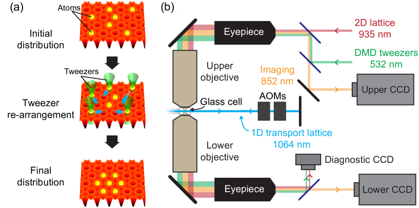
The QMS operates by assembling and patterning the sample via stereotactic manipulation of individual atoms. This is realized through highly coordinated and stable control of optical tweezers in combination with high resolution imaging of single atoms in an optical lattice. This capability will greatly increase the flexibility and fidelity of quantum simulation and allow for fast and efficient removal of entropy to prepare atoms in the quantum degenerate regimeWeiss et al. (2004). Moreover, in contrast to traditional cold atom experiments which typically study ground state or thermal equilibrium distributions of atoms, the QMS can tailor far-from-equilibrium, designer quantum states.
The operation of our QMS consists of three steps:
Step 1: Sample preparation. The QMS starts by collecting precooled Cs atoms in a magneto-optical trap (MOT), cooling them with degenerate Raman sideband cooling (dRSC), and then transferring them into a glass science cell using a moving 1D optical lattice. In the glass cell, the atoms are loaded into a 2D optical lattice, where each site has random occupancy.
Step 2: Ground state cooling and imaging. We first determine the atomic distribution in a deep 2D lattice based on site-resolving in situ imaging. During the imaging, the dRSC is employed to suppress tunneling and heating of the atoms. The photons emitted during cooling cycles are collected to image the site occupancies in the lattice (see Section VIII). With an imaging resolution of 655 nm, small compared to the lattice constant 881 nm, a high fidelity single site resolution can be reached.
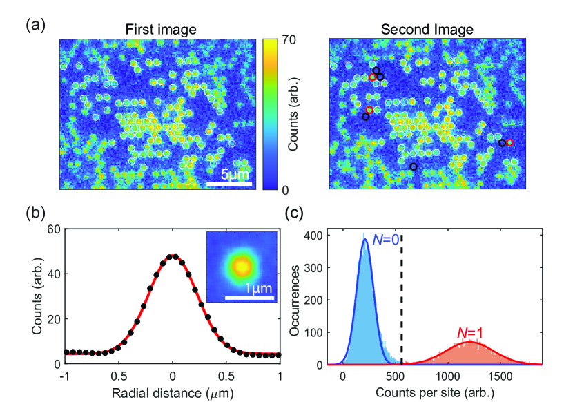
Step 3: Rearranging atoms. Based on the measured distribution in the lattices, we rearrange atoms into a desired pattern. To move the atoms to new locations, we use an array of optical tweezers at 532 nm prepared by a DMD. We first tune up the tweezer potential slowly to securely localize the atoms in the tweezer potential. We then drag atoms to new lattice sites adiabatically by video streaming a series of light patterns from the DMD. Throughout the relocation process, atoms are tightly confined in the tweezers to prevent tunneling. At the end of the process, atoms are released back to the lattice sites and cooled back to the ground state to remove excess entropy gained during the motion (see Fig. 1a).
III Mechanical structure and stability
In order to image, trap, and manipulate atoms at the site-resolved level, the relative mechanical stability between the optical lattice at 935 nm, the tweezer array at 532 nm, and the atom fluorescence at 852 nm must be kept within the spatial extent of the on-site wavefunction in our system (approx. 30 nm). To this end, we prepare the imaging, lattice, and tweezer beam paths such that all pass through the microscope optics in order to reduce their relative mechanical instability (see Fig. 1b).
The optical system is comprised of two identical microscopes placed symmetrically above and below the atom sample. The objectives (Special Optics, Inc.) are custom-designed to offer diffraction-limited performance at all the relevant wavelengths of 532 nm, 852 nm, and 935 nm. The objectives have a numerical aperture of and a working distance of 1.05 cm. This dual microscope configuration allows us to image the tweezer and lattice light using the diagnostic CCD in order to analyze the quality of the optical potentials on the atoms.
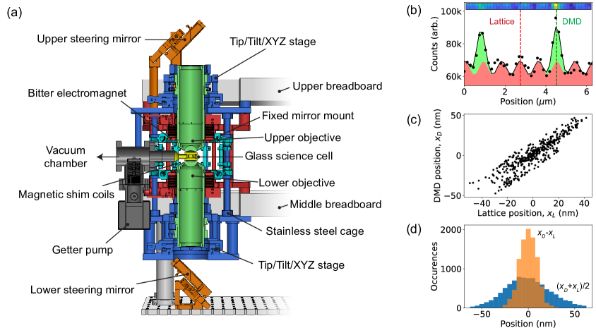
An ultra-stable stainless steel cage around the glass cell holds the two microscope objectives and other supporting components (Fig. 2a). By connecting the two objectives via a cage, the relative vibrational noise between these two sensitive optics is greatly reduced. In addition to the objectives, the stainless steel cage also supports auxiliary mirror mounts. A nearby water-cooled Bitter electromagnet is mounted on a separate structure to avoid acoustic noise caused by the water flow or large magnetic field quenchesSabulsky et al. (2013).
We test the relative mechanical stability of the 935 nm optical lattice and the 532 nm tweezers by imaging them on the lower diagnostic CCD at a fast frame rate of 650 Hz. By fitting the recorded images of the lattice sites and the tweezers, we track the variations of their positions and over time with high precision (see Fig. 2b). Details about the optical setup of the imaging, the lattice, and the tweezers can be found in Sections V and VI.
We observe that the two optical potentials experience highly correlated motion, indicating the common-mode behavior of the optical paths (see Fig. 2c). While and display a root-mean-square instability of 26 nm, their relative instability is only 9 nm (Fig. 2d), smaller than the expected on-site wavefunction extent. Thus, the small relative instability makes the QMS amenable to reliable arrangement of atoms in the lattice using tweezers.
IV Nanotextured glass cell
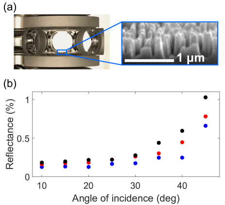
In order to maximize the optical transmission at wide acceptance angles for imaging, projection, and lattice formation at different wavelengths, we adopt a glass science cell (Precision Glassblowing Inc.) constructed with special nanotextured windows, rather than a traditional polymer-coated solution. The windows (TelAztec LLC) provide excellent broadband anti-reflection (AR) in the 532 nm to 1064 nm range for angles of incidence up to 45∘.
The glass cell window is textured with roughly 100 nm protuberances that have a large degree of randomness in the size and spacing, which contribute to their broadband, wide-angle AR performance (Fig. 3a). The nanotexturing provides a smooth transition in the index of refraction from air to glass, thus avoiding the large mismatch that causes strong reflections. These nanostructures are similar to the so-called “motheye" metamaterials that typically consist of a 2D array of pillars which are uniform in size and work well for narrowband applications Wilson and Hutley (1982); Hobbs et al. (2013).
We measure the window reflectivities (combined front- and back-reflections) at various wavelengths and verify that their reflectivity is or less at angles of incidence up to 45∘ (Fig. 3b). Lastly,we also note that due to the absence of polymer coating on the windows, the glass cell can be baked to higher temperatures in excess of C than the windows with dielectric coating, which promises better vacuum.
V 2D triangular lattice
Horizontal trapping of atoms in the glass cell is provided by a 2D triangular lattice formed by interfering three laser beams at wavelength 935 nm. Here 935 nm is a so-called “magic wavelength” for the Cs D2 transition at which atoms in the ground state and excited state experience the same lattice potential landscape Le Kien, Schneeweiss, and Rauschenbeutel (2013). A 1064 nm light sheet with the tight axis in the vertical direction compresses and holds the sample vertically.
In the lattice setup, we split one laser beam (SolsTiS, M Squared Lasers) into three beams each with 0.25 W of power, and send them off-axis downwards through the upper objective (Fig. 4a). They are aligned to be symmetric around the optical axis of the objective. After the glass cell window, the three beams propagate inwards with an angle of and intersect each other at a projected angle of 120∘ in the horizontal plane. The interference of the three beams creates a triangular optical lattice with an expected lattice constant of . The beam radius at the crossing point is approximately 40 m for all three beams. After passing through the atoms and the lower objective, the three lattice beams are directed to a diagnostic CCD for real-time monitoring of the lattice potential on the atom plane.
To achieve the deepest lattice potential, we set all beams to be circularly polarized (Fig. 4b) to maximize the polarization overlapping between all three beams. From the lattice beam parameters, we estimate a trap depth around , where is the recoil temperature. The lattice trap frequency is measured to be 75 kHz in the horizontal plane, consistent with our estimate.
The three beams share the same set of beam-shaping optics and propagate through almost-identical optical path lengths. This setup contributes to the phase stability of the optical lattice and the pointing stability of beams at the crossing point.
To confine atoms vertically, we apply a light sheet, which is a dipole trap formed by an elliptical Gaussian beam at 1064 nm with a power of 3 W (Mephisto MOPA, Coherent, Inc.) propagating along the -axis (Fig. 4a). The beam has a vertical waist of 3 m and a horizontal waist of 70 m, which provides a tight confinement in the vertical direction with an estimated trap frequency of 33 kHz, and a near-uniform intensity in the horizontal plane. From measurements of the vertical beam size and laser power, we estimate the trap depth to be 3 mK. The strong confinement ensures atoms are localized within the microscope’s short depth of focus of 1 m during the imaging.

VI DMD Tweezer Array

We rearrange atoms on the optical lattice using an array of mobile optical tweezers. The tweezers are formed by reflecting a 532 nm laser (Sprout-Solo, Lighthouse Photonics) with a digital micromirror device (DMD), which is capable of projecting arbitrary intensity patterns on the atoms at high speedsHa et al. (2015); Kim et al. (2016); Stuart and Kuhn (2018).
Our DMD (DLP4500, Texas Instruments) contains a 9121140 array of 7.64 m square mirrors that can quickly flip between an on- and an off-state. When a mirror is turned on, incident light is reflected into the upper microscope objective toward the atomic sample (Fig. 1b). Light reflected from off-mirrors is sent to a beam dump. Since 532 nm light is blue-detuned for the cesium transition, our tweezer array is formed by dark spots on a bright background (Fig. 5b). Due to diffraction effects related to the periodic structure of the mirrors, 60 of the incident power is directed toward the atoms.
We place the DMD in the image plane of the upper microscope objective, so that the pattern of on-mirrors matches the intensity profile imposed on the sample. In our system, approximately 10 DMD mirrors correspond to one lattice spacing of 881 nm, providing sufficient spatial resolution for smooth tweezer motion. Smooth motion is imperative to minimize the heating of atoms associated with discrete changes in the light intensity.
We characterize the resolution of the DMD projection system by imaging point-like patterns on the lower CCD at a wavelength of 532 nm. We fit the intensity pattern, which yields a near-diffraction-limited resolution of 450(25) nm based on the Rayleigh criterion (Fig. 5a).
High-fidelity control of the tweezer array requires fast updating of the DMD pattern with minimal delay time. To meet this requirement, we operate the DMD in a video-streaming mode where the computer treats the DMD as a display device (Fig. 5c). To improve the streaming bandwidth, we package every 24 binary tweezer patterns into a single 24-bit color image. The color images are then transmitted to the DMD at the maximum streaming rate of 105 Hz. For each color image, the DMD plays the constituent 24 binary patterns in sequence, thus reaching a final update rate of the tweezer patterns of 24105 Hz = 2.52 kHz. If we move the tweezers by translating their positions one micromirror at a time, then moving one atom to a neighboring site takes an estimated time of 4 ms, which is comparable to other tweezer rearrangement experiments Endres et al. (2016); Schymik et al. (2020). Lastly, we measure the total delay time to transmit images from the computer to DMD to be only 30 ms, which is short compared to the atom lifetime.
We measure the light reflected by the DMD on a fast photodiode in order to confirm the switching speed and playback quality. By alternating the DMD mirrors between on and off states at max speed we observe the expected 2.52 kHz refresh rate (Fig. 5d). We also confirm that long sequences of binary patterns are played in the correct order without pauses, skipping, or flickering Hueck et al. (2017).
VII Long Distance Optical Transport of Atoms
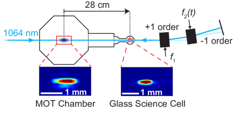
Our experiment starts with atoms pre-cooled in the MOT chamber before transferring them 28 cm to the glass cell (Fig. 6). To transport the atoms, we load them into a 1D optical lattice and move the lattice sites by shifting the frequency of one of the lattice beams (see Refs. Schmid et al., 2006; Klostermann et al., 2022).
The 1D transport lattice is formed using light at wavelength nm with 40 W of power (Mephisto MOPA, Coherent, Inc.) and the frequency shift is realized using two acousto-optic modulators (AOMs) in a double-pass configuration, see Fig. 6. When a detuning is applied to the second AOM drive, the retro-reflected beam is frequency shifted by , which results in the lattice sites acquiring a velocity equal to . This all-optical transport scheme does not require any moving parts, is insensitive to mechanical vibrations, and can proceed quickly with atoms in a deep lattice.
In the experimental sequence, atoms in the MOT chamber are first cooled by degenerate Raman sideband cooling and loaded into the transport lattice (250 K trap depth, 170 kHz trap frequency). Immediately after cooling, is smoothly increased to its final value of 600 kHz, reaching a max speed of 64 cm/s, after which it decreases back to zero so that the atom cloud gently comes to a stop at the center of the glass cell. We typically transport 2030 of the initial atom number in 400 ms to the glass cell and end with 6 atoms.
VIII Cooling and site-resolved imaging
Once atoms are transported into the glass cell, they are cooled into the 2D triangular lattice using dRSC. Photons emitted during the cooling process are collected by the microscope objectives to produce site-resolved images of atoms on the CCDs.
After atom transport we perform an initial dRSC stage to cool the sample into the 2D triangular lattice. The dRSC scheme closely follows Ref. Kerman et al., 2000. In our system, the lattice beams as described in Section V provide both the trapping potential and the Raman coupling necessary to reduce the vibrational energy. Circularly polarized optical pumping () and repumping () beams are applied in the same direction as the magnetic field to complete the cooling cycle. The magnetic field is in the horizontal plane bisecting the - and -axes as shown in Fig. 4b. After cooling the sample for 20 ms, we reach a temperature of 5 K in the lattice.
Following the initial cooling stage, the light sheet power is ramped up in 2 ms to compress the sample vertically into a thin layer. The lattice potential is then ramped down to release excess atoms outside of the light sheet. We then ramp the lattice power back up and perform a second dRSC stage. During cooling, pairs of atoms are ejected via light-assisted collisions, resulting in each lattice site having only zero or one atoms. Within 50 ms, the atoms are cooled near the 3D vibrational ground state after which we expose the CCDs to collect the photons.
A typical imaging exposure time is 200 ms, wherein an estimated 10 of the total emitted photons are collected on each of the upper and lower CCDs (iKon-M 934, Andor Technology Ltd) after accounting for the finite solid angle of the objectives and transmission losses. We can take 8 or more images per experimental cycle in order to study the loss and tunneling behavior over time. Fig. 7a shows an example of two consecutive exposures with a 5 ms hold time in between.
We analyze a central m region that contains approximately 200 lattice sites. Using a sparsely-filled sample, we can overlap the signal from single atoms to obtain the point spread function, which yields an imaging resolution of 655(3) nm based on the Rayleigh criterion. Our result is in agreement with the diffraction limit given by nm, where nm is the wavelength of the emitted photons (Fig. 7b).
We extract the positions of the lattice sites by taking the Fourier transform of the atom images. The sites are indicated with circular markers in Fig. 7a. We determine the lattice constants to be 845 nm, 860 nm, and 874 nm, all within 5 of our expectations. We attribute the discrepancies to imperfect lattice beam alignment.
We determine the atom occupancies by extracting the photon counts from each lattice site. In order to obtain higher fidelity, we perform image deconvolution using a kernel method Parsons (2016); Xu, Tao, and Jia (2014). With this method, a typical histogram of the photon counts is shown in Fig. 7c, and shows good separation between the distributions for sites with and without atoms. By fitting both distributions to Gaussians, we can set a threshold value to evaluate the site occupancies. The small Gaussian fits overlap suggests a high fidelity of 99 or an error rate of 1 from image reconstruction alone.
Our imaging allows us to study the particle dynamics over time by taking many images of the same atomic sample. By comparing adjacent images, we can identify changes in the site occupations, see Fig. 7a for an example. Disappearance of atoms in the later images is attributed to loss and hopping, while appearance of atoms in previously-unoccupied sites is likely due to hopping. The fidelity of atomic occupancies in two consecutive images is 91.4, limited by atom loss and tunneling.
IX Conclusion
In summary, we have presented the design and characterization of the quantum matter synthesizer, a novel cold atom quantum simulation platform that combines the clean trapping potential of a 2D optical lattice with the site-resolved control of atoms using an optical tweezer array.
Numerous innovative design elements were incorporated, including the nanotextured anti-reflective glass cell, the formation of a triangular lattice through the microscope objective, the long-distance atom transport with a 1D moving lattice, and the dual-objective microscope system. By combining the lattice and tweezer beams into the objective, we reach an exquisite mechanical instability below 10 nm, a small fraction of the on-site wavefunction extent. We also present a new type of dynamical tweezer array formed by a DMD that exhibits fast streaming speeds and low latency. Lastly, we demonstrate high-fidelity site-resolved imaging of Cs atoms in a 2D triangular lattice with relatively small exposure times of 200 ms. Through these technical developments, the QMS is well-positioned to simulate many-body physics with precise state preparation and measurement fidelity.
Author Declarations
The authors have no conflicts to disclose.
Author Contributions
J.T. designed and constructed the experiment, collected and analyzed data, and prepared the manuscript. M.Z. contributed to the construction of the experiment, collected and analyzed data, and prepared the manuscript. L.W. helped prepare the manuscript. C.C. supervised the project.
Acknowledgments
We thank Gustaf Downs, Mickey McDonald, Kai-Xuan Yao, and Paloma Ocola for early work on the design and construction of the system. We also thank Mykhaylo Usatyuk and Samir Rajani for characterization of the DMD. This material is based upon work supported by the U.S. Department of Energy, Office of Science, Office of Basic Energy Sciences, under Award Number DE-SC0019216 and by the National Science Foundation Graduate Research Fellowship under Grant No. DGE 1746045.
Data Availability
The data that support the findings of this study are available from the corresponding author upon reasonable request.
References
- Altman et al. (2021) E. Altman, K. R. Brown, G. Carleo, L. D. Carr, E. Demler, C. Chin, B. DeMarco, S. E. Economou, M. A. Eriksson, K.-M. C. Fu, et al., “Quantum simulators: Architectures and opportunities,” PRX Quantum 2, 017003 (2021).
- Schäfer et al. (2020) F. Schäfer, T. Fukuhara, S. Sugawa, Y. Takasu, and Y. Takahashi, “Tools for quantum simulation with ultracold atoms in optical lattices,” Nature Reviews Physics 2, 411–425 (2020).
- Esslinger (2010) T. Esslinger, “Fermi-Hubbard physics with atoms in an optical lattice,” Annu. Rev. Condens. Matter Phys. 1, 129–152 (2010).
- Gross and Bloch (2017) C. Gross and I. Bloch, “Quantum simulations with ultracold atoms in optical lattices,” Science 357, 995–1001 (2017).
- Kaufman and Ni (2021) A. M. Kaufman and K.-K. Ni, “Quantum science with optical tweezer arrays of ultracold atoms and molecules,” Nature Physics 17, 1324–1333 (2021).
- Greiner et al. (2002) M. Greiner, O. Mandel, T. Esslinger, T. W. Hänsch, and I. Bloch, “Quantum phase transition from a superfluid to a Mott insulator in a gas of ultracold atoms,” Nature 415, 39–44 (2002).
- Gemelke et al. (2009) N. Gemelke, X. Zhang, C.-L. Hung, and C. Chin, “In situ observation of incompressible Mott-insulating domains in ultracold atomic gases,” Nature 460, 995–998 (2009).
- Bakr et al. (2010) W. S. Bakr, A. Peng, M. E. Tai, R. Ma, J. Simon, J. I. Gillen, S. Foelling, L. Pollet, and M. Greiner, “Probing the superfluid–to–Mott insulator transition at the single-atom level,” Science 329, 547–550 (2010).
- Guardado-Sanchez et al. (2018) E. Guardado-Sanchez, P. T. Brown, D. Mitra, T. Devakul, D. A. Huse, P. Schauß, and W. S. Bakr, “Probing the quench dynamics of antiferromagnetic correlations in a 2D quantum Ising spin system,” Physical Review X 8, 021069 (2018).
- Brantut et al. (2012) J.-P. Brantut, J. Meineke, D. Stadler, S. Krinner, and T. Esslinger, “Conduction of ultracold fermions through a mesoscopic channel,” Science 337, 1069–1071 (2012).
- Preiss et al. (2015) P. M. Preiss, R. Ma, M. E. Tai, A. Lukin, M. Rispoli, P. Zupancic, Y. Lahini, R. Islam, and M. Greiner, “Strongly correlated quantum walks in optical lattices,” Science 347, 1229–1233 (2015).
- Aidelsburger et al. (2013) M. Aidelsburger, M. Atala, M. Lohse, J. T. Barreiro, B. Paredes, and I. Bloch, “Realization of the Hofstadter Hamiltonian with ultracold atoms in optical lattices,” Physical review letters 111, 185301 (2013).
- Zohar, Cirac, and Reznik (2015) E. Zohar, J. I. Cirac, and B. Reznik, “Quantum simulations of lattice gauge theories using ultracold atoms in optical lattices,” Reports on Progress in Physics 79, 014401 (2015).
- Cooper, Dalibard, and Spielman (2019) N. Cooper, J. Dalibard, and I. Spielman, “Topological bands for ultracold atoms,” Reviews of modern physics 91, 015005 (2019).
- Bakr et al. (2009) W. S. Bakr, J. I. Gillen, A. Peng, S. Fölling, and M. Greiner, “A quantum gas microscope for detecting single atoms in a Hubbard-regime optical lattice,” Nature 462, 74–77 (2009).
- Sherson et al. (2010) J. F. Sherson, C. Weitenberg, M. Endres, M. Cheneau, I. Bloch, and S. Kuhr, “Single-atom-resolved fluorescence imaging of an atomic Mott insulator,” Nature 467, 68–72 (2010).
- Lester et al. (2015) B. J. Lester, N. Luick, A. M. Kaufman, C. M. Reynolds, and C. A. Regal, “Rapid production of uniformly filled arrays of neutral atoms,” Physical review letters 115, 073003 (2015).
- Barredo et al. (2016) D. Barredo, S. De Léséleuc, V. Lienhard, T. Lahaye, and A. Browaeys, “An atom-by-atom assembler of defect-free arbitrary two-dimensional atomic arrays,” Science 354, 1021–1023 (2016).
- Endres et al. (2016) M. Endres, H. Bernien, A. Keesling, H. Levine, E. R. Anschuetz, A. Krajenbrink, C. Senko, V. Vuletic, M. Greiner, and M. D. Lukin, “Atom-by-atom assembly of defect-free one-dimensional cold atom arrays,” Science 354, 1024–1027 (2016).
- Lee, Kim, and Ahn (2017) W. Lee, H. Kim, and J. Ahn, “Defect-free atomic array formation using the hungarian matching algorithm,” Physical Review A 95, 053424 (2017).
- Omran et al. (2019) A. Omran, H. Levine, A. Keesling, G. Semeghini, T. T. Wang, S. Ebadi, H. Bernien, A. S. Zibrov, H. Pichler, S. Choi, et al., “Generation and manipulation of Schrödinger cat states in Rydberg atom arrays,” Science 365, 570–574 (2019).
- Bluvstein et al. (2022) D. Bluvstein, H. Levine, G. Semeghini, T. T. Wang, S. Ebadi, M. Kalinowski, A. Keesling, N. Maskara, H. Pichler, M. Greiner, et al., “A quantum processor based on coherent transport of entangled atom arrays,” Nature 604, 451–456 (2022).
- Liu et al. (2019) L. R. Liu, J. D. Hood, Y. Yu, J. T. Zhang, K. Wang, Y.-W. Lin, T. Rosenband, and K.-K. Ni, “Molecular assembly of ground-state cooled single atoms,” Phys. Rev. X 9, 021039 (2019).
- Young et al. (2022) A. W. Young, W. J. Eckner, N. Schine, A. M. Childs, and A. M. Kaufman, “Tweezer-programmable 2D quantum walks in a Hubbard-regime lattice,” arXiv preprint arXiv:2202:01204 (2022).
- Weiss et al. (2004) D. Weiss, J. Vala, A. Thapliyal, S. Myrgren, U. Vazirani, and K. Whaley, “Another way to approach zero entropy for a finite system of atoms,” Physical Review A 70, 040302 (2004).
- Sabulsky et al. (2013) D. O. Sabulsky, C. V. Parker, N. D. Gemelke, and C. Chin, “Efficient continuous-duty bitter-type electromagnets for cold atom experiments,” Review of Scientific Instruments 84, 104706 (2013).
- Wilson and Hutley (1982) S. Wilson and M. Hutley, “The optical properties of’moth eye’antireflection surfaces,” Optica Acta: International Journal of Optics 29, 993–1009 (1982).
- Hobbs et al. (2013) D. S. Hobbs, B. D. MacLeod, E. Sabatino III, J. A. Britten, and C. J. Stolz, “Contamination resistant antireflection nano-textures in fused silica for laser optics,” in Laser-Induced Damage in Optical Materials: 2013, Vol. 8885 (International Society for Optics and Photonics, 2013) p. 88850J.
- Le Kien, Schneeweiss, and Rauschenbeutel (2013) F. Le Kien, P. Schneeweiss, and A. Rauschenbeutel, “Dynamical polarizability of atoms in arbitrary light fields: general theory and application to cesium,” The European Physical Journal D 67, 1–16 (2013).
- Ha et al. (2015) L.-C. Ha, L. W. Clark, C. V. Parker, B. M. Anderson, and C. Chin, “Roton-maxon excitation spectrum of bose condensates in a shaken optical lattice,” Physical review letters 114, 055301 (2015).
- Kim et al. (2016) H. Kim, W. Lee, H.-g. Lee, H. Jo, Y. Song, and J. Ahn, “In situ single-atom array synthesis using dynamic holographic optical tweezers,” Nature communications 7, 1–8 (2016).
- Stuart and Kuhn (2018) D. Stuart and A. Kuhn, “Single-atom trapping and transport in dmd-controlled optical tweezers,” New Journal of Physics 20, 023013 (2018).
- Schymik et al. (2020) K.-N. Schymik, V. Lienhard, D. Barredo, P. Scholl, H. Williams, A. Browaeys, and T. Lahaye, “Enhanced atom-by-atom assembly of arbitrary tweezer arrays,” Phys. Rev. A 102, 063107 (2020).
- Hueck et al. (2017) K. Hueck, A. Mazurenko, N. Luick, T. Lompe, and H. Moritz, “Note: Suppression of kHz-frequency switching noise in digital micro-mirror devices,” Review of Scientific Instruments 88, 016103 (2017).
- Schmid et al. (2006) S. Schmid, G. Thalhammer, K. Winkler, F. Lang, and J. H. Denschlag, “Long distance transport of ultracold atoms using a 1D optical lattice,” New Journal of Physics 8, 159 (2006).
- Klostermann et al. (2022) T. Klostermann, C. R. Cabrera, H. von Raven, J. F. Wienand, C. Schweizer, I. Bloch, and M. Aidelsburger, “Fast long-distance transport of cold cesium atoms,” Physical Review A 105, 043319 (2022).
- Kerman et al. (2000) A. J. Kerman, V. Vuletić, C. Chin, and S. Chu, “Beyond optical molasses: 3D Raman sideband cooling of atomic cesium to high phase-space density,” Phys. Rev. Lett. 84, 439–442 (2000).
- Parsons (2016) M. F. Parsons, Probing the Hubbard model with single-site resolution, Ph.D. thesis, Harvard University (2016).
- Xu, Tao, and Jia (2014) L. Xu, X. Tao, and J. Jia, “Inverse kernels for fast spatial deconvolution,” in European Conference on Computer Vision (Springer, 2014) pp. 33–48.