Micromagnetics of magnetic chemical modulations in soft-magnetic cylindrical nanowires
Abstract
We analyze the micromagnetics of short longitudinal modulations of a high-magnetization material in cylindrical nanowires made of a soft-magnetic material of lower magnetization such as permalloy, combining magnetic microscopy, analytical modeling, and micromagnetic simulations. The mismatch of magnetization induces curling of magnetization around the axis in the modulations, in an attempt to screen the interfacial magnetic charges. The curling angle increases with modulation length, until a plateau is reached with nearly full charge screening for a specific length scale , larger than the dipolar exchange length of any of the two materials. The curling circulation can be switched by the Oersted field arising from a charge current with typical magnitude for a diameter of , and reaching a maximum for .
I Introduction
Cylindrical magnetic nanowires can be synthesized rather easily by electrodeposition in insulating templates with pores, such as ion-track-etched polycarbonate membranes [1] and anodized aluminum foils and thin films [2]. Such wires have attracted intense and continuous interest over the past three decades, partially for being a realization of a nearly one-dimensional magnetic system and thus a text-book case to understand fundamental phenomena. A wealth of phenomena have been investigated in cylindrical magnetic nanowires: current-perpendicular-to-plane giant magneto-resistance and measurements of spin diffusion length [3, 4, 5], ferromagnetic resonance [6], competition between shape and magnetocrystalline anisotropy [7], dipolar interactions in a dense and complex medium [8, 9, 10], nucleation at their apex [11, 12, 13, 14], statics and dynamics of domain-wall motion both under magnetic field and under a spin-polarized current [5, 15, 16, 17, 18, 19].
The versatility of cylindrical nanowires is high, with free choice of the composition and geometry, with diameters ranging from a few nanometers up to hundreds of nanometers, and lengths from a few tens of nanometers to tens of micrometers [1, 2, 20]. In addition, it is possible to vary features along their length, either through the modulation of their diameter [21, 22, 23, 24, 25, 26, 27, 28, 29, 30, 31, 32] or modulation of their composition [33, 34, 35, 36, 37, 38, 39, 40, 41, 42, 43]. The later is particularly interesting for engineering the longitudinal energy landscape and controlling domain-wall motion. From a fundamental point of view, this provides text-book cases of domain wall(DW) pinning on different types of defects [44, 45], related to the long-standing problem called the Brown paradox [44, 45]. For applications it may provide ways to enhance coercivity, contributing to the search for rare-earth-free permanent-magnet materials [46], design non-reciprocal ratchet-type devices [47], or provide a building block material for the concept of a domain-wall-based race-track memory [48, 49].
For spintronics, modulations of composition are preferable to modulations of diameter as they avoid local changes in the current density [28]. There are already several theoretical and experimental investigations of nanowires modulated in composition, addressing the physics of magnetization reversal [50, 47, 51, 37, 52, 53, 54], domain-wall pinning [55, 50, 33] or field-driven domain wall motion [55, 47, 35, 36]. Yet, the underlying physics of these modulations has not been examined in detail.
Here, we report the micromagnetics of chemical insertions within cylindrical nanowires. Although the insertions have higher magnetization than the rest of the nanowire, all materials considered are magnetically soft. Thus the materials of choice for the segments out of the chemical insertions are typically composed of Ni-rich, CoNi or FeNi alloys, which come with rather low magnetization. The nanowires are uniformly magnetized along their axis outside the modulations, that is, we are not considering domain walls. We consider the practical case of Fe80Ni20 chemical modulations periodically inserted in Permalloy (Ni80Fe20), yet we draw conclusions in terms of reduced magnetic quantities when applicable, for the sake of generality. We combine simulations, micromagnetic modeling and experiments aiming to provide a comprehensive view, which we hope can be useful as a firm ground for the understanding of more complex situations involving chemical modulations, such as their interaction with magnetic domain walls.
II Methods
II.1 Experimental methods
Permalloy (Fe20Ni80) cylindrical nanowires with nanometer-sized modulations of composition Fe80Ni20 were synthesized by template-assisted electrochemical deposition. Two different nanoporous anodic aluminum oxide (AAO) templates were prepared. First, AAO templates with pore diameter ranging between were prepared by one-step hard anodization of Al disks (Goodfellow, in purity) in a water-based solution of oxalic acid () and ethanol (), applying of anodization voltage at for . Second, AAO templates with pore diameter below 100 nm were prepared by two-step anodization in oxalic acid (), applying of anodization voltage at for and for the first and second anodization respectively. In both cases, the remaining Al was etched with an aqueous solution of CuCl2 () and HCl (), the oxide barrier was removed and the pores were opened to the final diameter with H3PO4 (5 % vol.). In some cases we performed HfO2 atomic layer deposition (ALD) coating of the pores to optimize the synthesis and prevent sample oxidation. However, this is not a key step because all the nanowires, also the ones without coating, have an oxidized CrO layer created by the solution used to release the nanowires from the alumina template. Therefore, at the end all the samples are protected from strong oxidation due to this
The nanowires were grown using pulse-plating electrodeposition under conditions similar to those described in Ref. [55]. The width of the pulses was varied to change the length of the chemical modulation from , and the length of the Permalloy segments is a few hundreds of nanometers to several micrometers. Following growth, the templates were dissolved in H3PO4() and H2CrO4(). Then, the nanowires were dispersed on Si substrates, either bulk or with a Si3N4 window to allow for transmission microscopy. Nanowires were contacted electrically using laser lithography in order to allow current injection. Resistivity values obtained are as low as at room temperature in comparison with of bulk Permalloy despite the material interfaces, allowing the injection of currents much higher than . The residual resistivity value measured at low temperature is .
We used several types of magnetic microscopy techniques in order to access three-dimensional magnetization textures, all based on x-ray magnetic circular dichroism (XMCD): photo emission electron microscopy (PEEM) in shadow mode [16, 56, 57] and transmission x-Ray microscopy (TXM) [58] at CIRCE and MISTRAL beamlines of ALBA Synchrotron, Scanning transmission x-Ray microscopy (STXM)[59] and ptychography[60, 61, 62] at HERMES beamline of SOLEIL synchrotron. Unless otherwise stated, we set the photon energy at the Fe L3 absorption edge. The x-ray beam direction was typically nearly transverse to the nanowire axis, in order to be mostly sensitive to non-longitudinal components of the magnetization. For PEEM and TXM microscopy, series of about 64 images per polarity were taken and registered to increased the signal-to-noise ratio, while keeping under control the loss of spatial resolution due to drift during long acquisitions. For STXM, an image is reconstructed from a single scan. In the case of ptychography, an overlap of 30 % of the illumination spots allowed a rather fast convergence of the iterative algorithm, and a reconstructed amplitude image of sub- resolution. Ptychographic reconstruction was carried out using the open-source PyNX software developed at the European Synchrotron Radiation Facility [63]. Complementary measurements were performed by atomic and magnetic force microscopy (AFM and MFM respectively), as well as by scanning transmission electron microscopy (STEM) and holography.
II.2 Theoretical methods
Micromagnetic simulations were performed using feeLLGood [64, 65, 66], a homemade finite-element-based code that uses tetrahedrons for the discrete mesh. The system considered is a cylindrical nanowire made of two Permalloy segments of (for a diameter ) or (for ) length each, separated by a Fe80Ni20 chemical modulation with length varied between 20 and . In order to mimic an infinite wire, the magnetic charges at the wire ends are removed numerically. The mesh size used was . The following material parameters were used: spontaneous magnetization for the Permalloy segments, for the Fe80Ni20 modulation, for the Fe65Ni35 modulation, single exchange stiffness for all materials and zero magnetocrystalline anisotropy. The reason to use a single value for exchange stiffness is to highlight the impact of the variation of on the micromagnetics, which is the driving force for the phenomena reported here. The resulting dipolar exchange lengths are , and , respectively. Finally, a damping coefficient equal to 1 was used for faster relaxation and dynamics. When considering the effect of an Œrsted field we consider a uniform and steady charge current flowing along the wire axis , disregarding spin-transfer torque effects.
Post-processing scripts were used to extract quantitative information on the magnetization components from simulated and experimental data. From magnetic contrast images the degree of tilt of the magnetization was extracted based on the Beer-Lambert law as described in Ref. [67] (see Supplemental Material for a detailed description).
III RESULTS
III.1 Experimental evidence of stray field
The insertion of chemical modulations with high magnetization within a Permalloy nanowire is expected to affect the magnetostatics of the system. Indeed, when the magnetization of the nanowire lies along its axis, as expected for soft magnetic materials in elongated structures, surface magnetic charges are expected to appear at the interface between the two materials, due to the mismatch of magnetization.
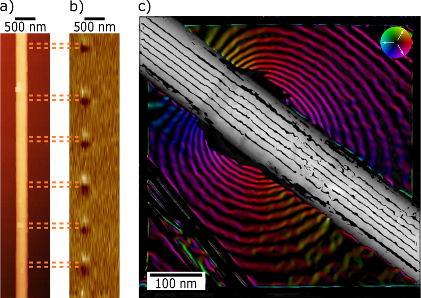
Fig. 1a-b show an AFM and a MFM image of a nanowire with and , in a remanent state. In the MFM image, a bipolar magnetic contrast is observed at each modulation. This suggests the existence of opposite directions of the vertical magnetic stray field on either side of the modulation, which is consistent with the expectation of opposite magnetostatic charges at the two interfaces.
The stray field can be visualized directly with electron holography. The location of the modulations was determined first, by imaging in STEM, highlighting the contrast. The stray field, imaged by electron holography, takes the form of a flux leakage at the modulation, opposite to the direction of magnetization in the wire (Fig. 1c). For this specific case, the stray field is slightly shifted to the left due to a material defect on this particular wire. Note the continuity of the magnetic induction field inside the wire, expected from Maxwell’s equations. Yet, magnetic induction results both from magnetization and from the magnetostatic field, so that the details of the magnetization distribution cannot be easily obtained from this image. More is reported in the next section with other imaging techniques that are directly sensitive to the magnetization .
III.2 Experimental evidence of curling
Imaging techniques based on x-ray magnetic dichroism are complementary to electron holography. Indeed, the latter is sensitive to the two components of magnetic induction perpendicular to the beam, while the former directly probes the magnetization component along the beam. Therefore, the combination of both provides a pretty good view of the three-dimensional distribution of magnetization.
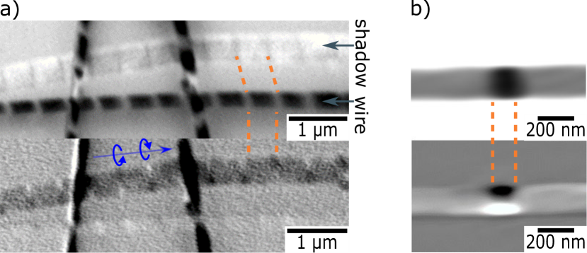
Fig. 2a shows a shadow PEEM image of a nanowire with . This specific wire is incidentally lying on top of two other wires, making its shadow fully visible. Shadows are stretched by about a factor of 3.5 along the beam direction due to the near grazing x-ray incidence (angle of ). The sample was rotated to have the nanowire almost perpendicular to the x-ray beam.
The top image is the subtraction of two x-ray absorption spectroscopy (XAS) images at the Fe and Ni L3 edges, highlightling the changes in chemical composition. The Fe-rich chemical modulations appear bright (more electrons emitted) and dark (fewer photons transmitted) on the wire and the shadow, respectively. The bottom image is the corresponding XMCD image. The lack of magnetic contrast in the Permalloy segments reveals that the magnetization lies along the wire axis, consistent with the electron holography results (Fig. 1c). However, magnetic contrast is observed at the modulations, mostly in the shadow as surface oxidation masks magnetic contrast on the wire surface. The bipolar dark and bright contrast at the modulations reflects components of magnetization parallel and anti-parallel to the X-ray beam on opposite sides of the wire. Such features are often called curling [68] in micromagnetism. The curved blue arrows in Fig. 2a shows that the sign of curling, which we will call circulation, can be either positive or negative in the same wire. The distribution of magnetization in the chemical modulations observed with higher spatial resolution by XMCD ptychography is shown in Fig. 2b. Note that in this case the aspect ratio along the transmitted x-ray beam is equal to one. We imaged nanowires with and , and evidenced curling in all of them. It should be noted that curling magnetization at the chemical modulations cannot be viewed as a 360∘ domain wall since the integration of change of magnetization angle along the axial direction is zero instead of 2, which is the expected value for a 360∘ domain wall.
III.3 Analytics to explain the physics of curling
Curling around the axis is a well-known feature of wires: for above typically seven times the dipolar exchange length, a mostly uniformly-magnetized wire ends up with such a curling feature at each end [11, 14, 69]. Similar to the curling reversal mode from which the name was first coined [68], this results from the driving force of surface charges, which appear at each end of the wire with areal density in the case of uniform axial magnetization. For the following discussion, it is important to realize that curling does not remove magnetic charges from the system, whose integrated value is fixed by topology. Instead, curling converts part of the surface charges into volume charges . These are on average further apart from each other than surface charges, thereby lowering the total magnetostatic energy of the system. In practice, the amount of curling is determined by the balance of gain in magnetostatic energy versus the cost in exchange energy. Another analogous situation is that of the vortex state in disks and short cylinders.
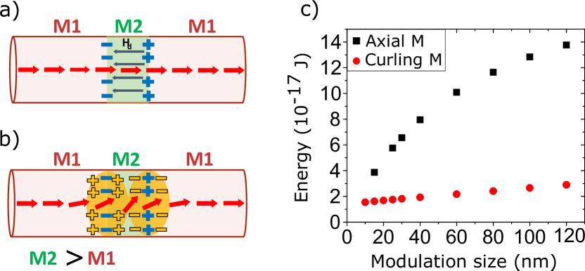
A chemical modulation with high magnetization can be described in similar terms. The mismatch of spontaneous magnetization across the interfaces gives rise to surface charges of areal density at the interfaces (Fig. 3a). As a result, magnetization tends to curl at the modulation, reducing longitudinal magnetization, its interfacial mismatch, and the associated dipolar energy. The volume density of charge resulting from the gradient of longitudinal magnetization has a sign opposite to that of the nearby interfacial charges (Fig. 3b), which can be understood as a screening effect. The initially dipolar nature of magnetostatics at the modulation tends to be replaced by an octopole, largely decreasing the extent of the resulting magnetostatic field, and thus its energy. It is important to remark that this occurs when the chemical modulation has a higher magnetization than the rest of the nanowire . For the opposite case, no screening mechanism may occur since surface and volume charges have the same sign (for more details see the Supplementary Material).
We propose several assumptions in order to model the physics of charge screening analytically in a simple manner and predict general features. In a first stage we consider just one interface, which would stand for a very long modulation: the domain material for , and modulation material for . Second, we consider a system with large diameter (), which allows us to neglect the radial and azimuthal contributions to exchange. The corolla of the second hypothesis is that the dominating contribution to the energy of the system is magnetostatics, so that as a third hypothesis we assume complete screening, i.e., exact compensation of the total amount of surface charge with volume charges of opposite sign. This is expected to bring the magnetostatic energy to a minimum. Fourth, we neglect any radial magnetization component.
We define the curling angle as the angle of magnetization away from the axial direction and towards the azimuthal direction (inset of Fig. 5a). As magnetization must remain longitudinal on the axis, the curling angle must be dependent on the distance to the axis. We use an ansatz to describe the variation of the curling angle along :
| (1) |
where is the wire radius, is the distance to the axis, and is the coordinate along the wire axis. This ansatz accurately describes the spatial variation of along [70, 67], minimizing the (residual) exchange energy. The magnetization state of the system is then fully determined by the function , with in the axially magnetized domain. In this simplified example, stands for the final curling angle at the surface at a distance sufficiently far from the interface.
The Appendix provides the details of the model. In short, we use the following procedure: i) We set to a given value, not known at this stage. From this we compute the total surface charge at the interface, and the integrated volume charges on the left-hand side of the modulation. ii) We assume an equal share of volume charges on either side of the interface, which allows us to derive the peripheral curling angle far inside the modulation, away from the interface, , needed to establish these volume charges. This assumption is made with the aim of maximizing the gain provided by the screening of surface charges or, in other words, to obtain the largest screening for a given number of surface charges. iii) We impose full screening of charges in a quadrupolar fashion, i.e., the integrated interfacial and volume charges compensate. This sets the values and self-consistently. In the end we find:
| (2) | |||||
| (3) |
Based on the expansion , we can rewrite these two equations for the longitudinal magnetization:
| (4) | |||||
| (5) |
Note that the model yields the curling angle at the interface and deep inside the modulation ( in the model), however not the full function . Also, the above expressions depend only on , because the model disregards exchange. Before assessing the validity of the model and hence its physical basis with micromagnetic simulations, let us make a few sanity checks. i) There is no curling without a material modulation, i.e., for ii) mimicks the situation of the apex of a cylindrical nanowire. In this situation we get , which is slightly more than , the expectation to cancel surface charges. This comes from the hypothesis of the global compensation of charges: as no volume charge is created close to the axis for which magnetization remains longitudinal, more charges need to be created away from the axis. We will come back to this when comparing the model wnumerical micromagnetics.
Coming back to the specific case of Permalloy segments with modulations of inverted composition, on the basis of our model we expect the following: [] and [].
III.4 Micromagnetic simulation of curling
The model reported in the previous paragraph intends to highlight the main physical ingredients driving curling, and to allow a quick estimation of the resulting angle. Here, we report a series of micromagnetic simulations to asses the validity of the model, refine its predictions quantitatively, and address the situation of a finite-length modulation, which cannot be tackled as easily through analytic modeling.
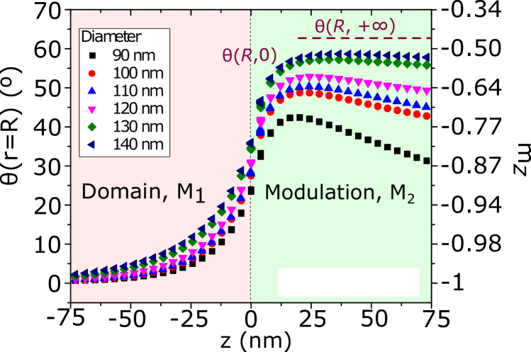
Fig. 4 shows the curling profile at the surface , across a single interface between two materials with semi-infinite length derived from micromagnetic simulations. This is the situation considered in the model, whose predictions are indicated with horizontal dashed lines and a cross. It is clear that the model overestimates the curling angle, yet the agreement is better for larger diameter. This is because the model disregards exchange, while the energy cost coming from radial exchange decreases for larger diameter. We expect that other effects limiting curling are the fact that screening is non-local, as mentioned in the previous paragraph, balancing volume versus surface, and that magnetization cannot curl close to the wire axis. Yet, the very good quantitative agreement for curling inside the modulation for large diameter confirms that charge screening is indeed the key ingredient driving curling. The agreement for curling at the interface is not as good, although in both cases . The reason is that volume charges are related to the variation of longitudinal magnetization, which does not scale linearly with the curling angle, as the right -axis in the plot reflects. Finally, note that curling tends to decrease in the modulation, when moving away from the interface. The reason is that the radial exchange cost of curling scales linearly with once the curling angle has reached a plateau, while it provides no further screening benefit. In the case of a semi-infinite medium, magnetization would progressively turn back fully axial for - an effect that is not reflected by the analytical model due to the disregard of exchange. The faster decay of curling for smaller diameter is consistent with this picture.
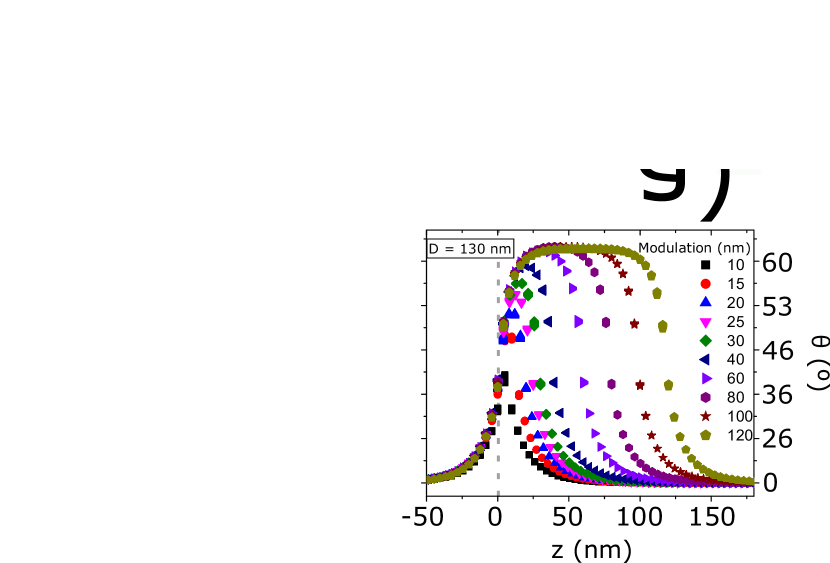
We now turn to the case of practical interest: a material modulation with finite length. Fig. 5a-b illustrate the surface and cross-sectional views of a simulated micromagnetic state at rest. The graphs in Fig. 5c-d show the peripheral profile and curling angle, , versus axial position for two wire diameters, and , each for a series of values. The grey dashed line indicates the start of the chemical modulation at .
For long modulations the curling angle reaches a plateau, with a value very similar to the case of a single interface (Fig. 4). Yet, the curling angle tends to decrease as increases due to an increasing cost in exchange. Thus, a maximum curling angle is found for a given modulation length: for , with , , and for , with . Note that curves have nearly an inversion symmetry across each interface, unlike curves. Since volume magnetic charges are related to the variation of , this inversion symmetry shows that screening is largely symmetric.
The curling angle plateau is not reached for modulations shorter than typically . There is no energy dependence of the chirality of the system, i.e., circulation versus longitudinal magnetization, so that both circulations have the same energy, which requires a certain distance to rotate magnetization. This competition defines the dipolar exchange length , dictating a maximum gradient of magnetization direction. More precisely, with the definition , magnetization may rotate by over a distance . It can be seen on Fig. 5c-d that all curves overlap at their rising stage in the Permalloy segment, even if the plateau is not reached. From the angular gradient in Fig. 4, we derive the characteristic length scale specific to a modulation as the distance that would be required to rotate magnetization by , , much larger than the dipolar exchange length of any of the two materials. We believe that the reason is twofold: first, the charges scale like , not with the full magnetization; second, the screening effect on both sides of the interface further decreases the effective charge and thus the magnetostatic energy.
Micromagnetic simulations also allow us to derive the energy of the system for any distribution of magnetization. Fig. 3c shows the total micromagnetic energy versus modulation length, for longitudinal uniform magnetization and for the relaxed curling state for a 130 nm diameter wire. It is clear that curling allows to decrease energy, which however has a lower limit imposed by the residual magnetostatic energy and the resulting exchange energy. The graph also illustrates how the gain is less for short modulations, consistent with the decrease in curling (Fig. 5).
III.5 Curling controlled by applied magnetic fields
III.5.1 Response to an axial magnetic field
We performed high spatial resolution magnetic imaging by XMCD-ptychography in order to experimentally confirm the predictions of the previous section. Since the magnitude of curling depends on the materials parameters and the modulation length, which may all suffer from experimental errors, we studied both the curling angle at rest and its response to an external static magnetic field along the wire axis for a more robust comparison. We conducted experiments under a magnetic field up to applied perpendicular to the x-ray beam and thus almost along the nanowire’s axis. A small angular offset of was chosen in order to have a small dichroic contribution from the axial magnetization and thus distinguish the magnetization direction in the domains (Fig. 6a).
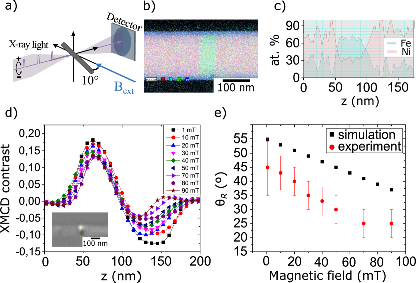
The nanowire chosen for this study has and . The experimental results and their analysis are summarized in Fig. 6. In Fig. 6d, we show the line profile of the XMCD contrast across the wire, centered on the modulation (yellow line in the inset), for several applied magnetic fields. Its non-centro-symmetric shape results from sample rotation away from the plane perpendicular to the x-ray beam. The conversion of these curves into the curling angle is performed taking into account the intrinsic features (exponential absorption along the x-ray path, 3D magnetization texture) and the experimental considerations (finite size of the probe, background intensity) is explained in the Supplementary Material and in [67]. A crucial parameter of the model is the absorption coefficient of the material that depends on composition, which was independently obtained by electron-energy-loss- spectroscopy (EELS) measurements (Fig. 6b-c) as at the modulation on this specific nanowire. In Fig. 6e, the evolution of as a function of the applied magnetic field is shown for data extracted from the experiments (red symbols) and from micromagnetic simulations (black symbols). Curling decreases with applied field, however, it does not go to zero, owing to the large magnetostatic energy involved.
III.5.2 Œrsted field
We have seen experimentally that curling in the modulations may be either clockwise or anticlockwise (Fig. 2a). There is no energy dependence of the chirality of the system, i.e., circulation versus longitudinal magnetization, so that both circulations have the same energy. We expect that this degeneracy is lifted upon application of an electric current flowing along the wire, which gives rise to an Œrsted magnetic field that couples directly with curling, either parallel or antiparallel. This situation is analogous to the case of azimuthal curling around Bloch-point domain walls in nanowires, for which the Œrsted field has been proven to be crucial for the dynamic stability and switching [19, 70].
We conducted experiments on electrically-contacted nanowires, injecting current pulses of magnitude around , variable sign, and duration up to a few nanoseconds. The images were taken using XMCD-STXM or TXM, under static conditions before and after application of every current pulse. We evidence the existence of a threshold for the current density, above which the sign of curling in the modulation switches deterministically, if not initially parallel to the Œrsted field. The switching is illustrated in Fig. 7 for a wire with and . Fig. 7a shows an absorption image, highlighting the position and width of the modulation. The initial state, revealed by XMCD in b, has a negative circulation (yellow arrow) with respect the magnetization direction (black arrow). After the application of a current pulse with magnitude and duration , circulation has switched to a positive circulation state (Fig. 7c, yellow arrow). This is consistent with the sign of the Œrsted field associated with the charge current (red arrow). We evidenced no dependence of the switching with pulse duration for lengths . Open black and red symbols in Fig. 7d show the experimental dependence of the threshold current versus modulation length for and respectively. The calculation of the current density that flows through the wire was done taken into account the attenuation and losses of the electric pulse (see Supplemental Material).
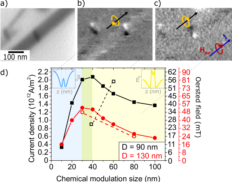
We performed micromagnetic simulations to shed light on the switching mechanism. We considered only the effect of the Œrsted field, disregarding spin-transfer torque (which was previously shown to be negligible [70]), as well as Joule heating, which plays a key role in magnetization dynamics for high current density values or long pulses. In our experiment we estimated a temperature rise of for a current density of magnitude , pulse duration and 90 nm diameter. The initial magnetization state prepared has a negative circulation with respect to the axial magnetization direction , as in Fig. 5a, antiparallel to the Œrsted field that will be applied. We need a criterion to determine the minimum current density required to switch the circulation. Indeed, since any computation time is finite, a long incubation time may be misinterpreted as absence of circulation switching. A standard method in micromagnetism to address this issue is to rely on the scaling of a parameter, such as the switching time above the threshold, versus the driving parameter, here the current density . The switching time was defined by the first occurrence of at the surface of the wire, which reflects the transition towards positive circulation. We expect and indeed evidence that scales nearly linearly with [70], from which is determined.
We considered lengths ranging from 20 to and two diameters: and . The results are summarized in Fig. 7d, along with the experimental results. One can see that the switching current is higher for smaller diameter. While the micromagnetic energetics may play a role, the dominant effect is probably the magnitude of Œrsted field. Indeed, it rises linearly with radius for a given density of current, thus promoting switching. In addition, the variation with modulation length is non-monotonous, displaying a maximum of switching current around for and around for . This hints at the existence of two distinct switching regimes, which we understand as follows. For short modulations, the curling angle (Fig. 5) as well as the energy barrier (Fig. 3c) decrease, so that switching is easier. For long modulations, the curling angle presents a minimum at the center of the modulation, which we understand as follows: While curling at the interfaces is driven by significant magnetostatic energy and the tendency for charge screening, curling at the center is imposed only through exchange with the two interfacial regions, which decays with modulation length once the plateau is reached. Thus, the central region is expected to be a weak locus for nucleation. Examination of snapshots of the magnetization distribution during the switching process, confirms that it occurs largely as a coherent process in cylindrical coordinates for short modulations, in terms of , while for long modulations the switching process is not coherent but rather with a profile that indicates nucleation at the center of the modulation. Insets in Fig. 7d show profiles at the periphery of the wire before the circulation reversal. In the short modulation regime (blue blackground) decreases more rapidily at the edges of the modulation than at the center (grey dashed lines in the inset) whereas in the long modulation regime (yellow background) this occurs at the center of the modulation. The high value of out of the modulation reflects the tilt of the Permalloy domains due to the Œrsted field (for more details see the Supplementary Material). We pointed out in the micromagnetics of the modulation at rest, that the characteristic length scale here is , in the case of modulations within segments. This means, magnetization may rotate by over a distance . As the plateau for curling reaches , so that the total rotation is twice this value, we expect that the length required is . This is consistent with the modulation width giving rise to the maximum of switching current (Fig. 7d), which confirms the relevance of a specific length scale for modulations, .
The order of magnitude for the switching current is consistent between simulations and experiments. However, while the experimental trend for is consistent with the above, for it is found to be opposite. Reasons can be several-fold. First, in the simulations we did not consider a distinct value for exchange stiffness in the modulation material, while a larger exchange is expected in practice for , which shall increase . Second, we have neglected thermal activation (expected to have more impact for shorter modulations and smaller diameters) as well as heating during the current pulse. Third, the modulation length and materials composition suffer from experimental uncertainties.
III.6 Conclusion
Combining experiments, analytical modeling and micromagnetic simulations, we provide a rather consistent qualitative and quantitative view of the micromagnetics of high-magnetization longitudinal material modulations in cylindrical nanowires. Their key feature is the spontaneous occurrence of curling around the axis, driven by the need to create volume magnetic charges and screen the interfacial charges between different materials. This replaces a net charge by a quadrupolar distribution for an interface, and the dipole of the total modulation by an octopole, thereby sharply decreasing the magnetostatic energy of the system. An analogy can be drawn with vortex states in disks and short cylinders, sharing the same feature of magnetization distribution, however with different quantitative energetics. We evidence a specific length scale, , a few times larger than the dipolar exchange length of any of the two materials and expected to scale with . For modulations shorter than typically the charge screening is partial, and switching of the curling sign with an Œrsted field occurs in a coherent fashion. For modulations longer than this, the charge screening is nearly complete, the curling reaches an angle that can be predicted analytically, and switching of the curling sign with an Œrsted field occurs incoherently, nucleating from the center of the modulation and expanding towards its interfaces. The switching current reaches its maximum at the cross-over between the two regimes. We believe that this knowledge of the micromagnetics at modulations is important in order to understand more complex situations, such as their interaction with magnetic domain walls.
III.7 Acknowledgments
We acknowledge support from the French RENATECH network, the team of the Nanofab platform (CNRS Néel institut), and the CNRS-CEA METSA French network (FR CNRS 3507). The project received financial support from the French National Research Agency (Grant No. ANR-17-CE24-0017-01) (MATEMAC-3D), from the Spanish MCIN/AEI/ 10.13039/501100011033 under grant PID2020-117024GB-C43 as well as by the Comunidad de Madrid (Spain) through the project NanoMagCOST (CM S2018/NMT-4321). Sandra Ruiz-Gómez gratefully acknowledges the financial suppport of the Alouexander von Humboldt foundation.
III.8 Data availability
Associated data is also available on https://doi.org/10.5281/zenodo.6532308.
IV Annex
Here, we detail intermediate steps supporting the analytical model, whose main features are described in section III.3.
Throughout the derivation of the analytical model, we make use of the following integrations:
| (6) |
| (7) | ||||
| (8) |
| (9) |
The latter two equations relate to the radial areal average, and make use of the expansion of to second order, i.e., up to .
The distribution of magnetic charges at the interface between the two materials reads:
| (10) |
Upon integration on the full disk cross-section, we find the resulting total charge, expanding the cosine up to second order:
| (11) |
The distribution of volume magnetic charges reads:
| (12) |
Upon integration along both the radius and the longitudinal coordinate , we derive the total volume charge:
| (13) | ||||
In the above, the first term in brackets on the right-hand side stands for volume charges in material 1, while the second term stands for charges in material 2. We now make the assumption that volume charges are equally shared on either sides of the interface, to achieve a quadrupolar distribution and minimize the energy of the system. This sets the condition:
| (14) |
and allows to simplify the expression for the total volume charges:
| (15) | ||||
We now equal the total interface and volume charges in absolute value [Eq.(11) and Eq.(15)], assuming full screening. This leads to the following expressions:
| (16) | |||||
| (17) |
Eq.(2) and Eq.(3) directly derive from the above, with a numerical approximation for .
References
- Fert and Piraux [1999] A. Fert and J. L. Piraux, Magnetic nanowires, J. Magn. Magn. Mater. 200, 338 (1999).
- Sousa et al. [2014] C. T. Sousa, D. C. Leitao, M. P. Proenca, J. Ventura, A. M. Pereira, and J. P. Araujo, Nanoporous alumina as templates for multifunctional applications, Appl. Phys. Rev. 1, 031102 (2014).
- Piraux et al. [1996] L. Piraux, S. Dubois, and A. Fert, Perpendicular giant magnetoresistance in magnetic multilayered nanowires, J. Magn. Magn. Mater. 159, L287 (1996).
- Dubois et al. [1999] S. Dubois, L. Piraux, J. M. George, K. Ounadjela, J. L. Duvail, and A. Fert, Evidence for a short spin diffusion length in permalloy from the giant magnetoresistance of multilayered nanowires, Phys. Rev. B 60, 477 (1999).
- Ebels et al. [2000] U. Ebels, A. Radulescu, Y. Henry, L. Piraux, and K. Ounadjela, Spin accumulation and domain wall magnetoresistance in 35 nm co wires, Phys. Rev. Lett. 84, 983 (2000).
- Ebels et al. [2001] U. Ebels, J. L. Duvail, P. E. Wigen, L. Piraux, L. D. Buda, and K. Ounadjela, Ferromagnetic resonance studies of ni nanowire arrays, Phys. Rev. B 64, 144421 (2001).
- Darques et al. [2005] M. Darques, L. Piraux, A. Encinas, P. Bayle-Guillemaud, A. Popa, and U. Ebels, Electrochemical control and selection of the structural and magnetic properties of cobalt nanowires, Appl. Phys. Lett. 86, 072508 (2005).
- De La Torre Medina et al. [2009] J. De La Torre Medina, M. Darques, L. Piraux, and A. Encinas, Application of the anisotropy field distribution method to arrays of magnetic nanowires, J. Appl. Phys. 105, 023909 (2009).
- Rotaru et al. [2011] A. Rotaru, J.-H. Lim, D. Lenormand, A. Diaconu, J. B. Wiley, P. Postolache, A. Stancu, and L. Spinu, Interactions and reversal-field memory in complex magnetic nanowire arrays, Phys. Rev. B 84, 134431 (2011).
- Da Col et al. [2011] S. Da Col, M. Darques, O. Fruchart, and L. Cagnon, Reduction of magnetostatic interactions in self-organized arrays of nickel nanowires using atomic layer deposition, Appl. Phys. Lett. 98, 112501 (2011).
- Zeng et al. [2000] H. Zeng, M. Zheng, R. Skomski, D. J. Sellmyer, Y. Liu, L. Menon, and S. Bandyopadhyay, Magnetic properties of self-assembled Co nanowires of varying length and diameter, J. Appl. Phys. 87, 4718 (2000).
- Fodor et al. [2002] P. S. Fodor, G. M. Tsoi, and L. E. Wenger, Fabrication and characterization of Co1-xFex alloy nanowires, J. Appl. Phys. 91, 8186 (2002).
- Zeng et al. [2002] H. Zeng, R. Skomski, L. Menon, Y. Liu, S. Bandyopadhyay, and D. J. Sellmyer, Structure and magnetic properties of ferromagnetic nanowires in self-assembled arrays, Phys. Rev. B 65, 134426 (2002).
- Wang et al. [2008] T. Wang, Y. Wang, Y. Fu, T. Hasegawa, H. Oshima, K. Itoh, K. Nishio, H. Masuda, F. S. Li, H. Saito, and S. Ishio, Magnetic behavior in an ordered Co nanorod array, Nanotechnology 19, 455703 (2008).
- Biziere et al. [2013] N. Biziere, C. Gatel, R. Lassalle-Balier, M. C. Clochard, J. E. Wegrowe, and E. Snoeck, Imaging the fine structure of a magnetic domain wall in a Ni nanocylinder, Nano Lett. 13, 2053 (2013).
- Da Col et al. [2014] S. Da Col, S. Jamet, N. Rougemaille, A. Locatelli, T. O. Menteş, B. S. Burgos, R. Afid, M. Darques, L. Cagnon, J. C. Toussaint, and O. Fruchart, Observation of bloch-point domain walls in cylindrical magnetic nanowires, Phys. Rev. B 89, 180405 (2014).
- Da Col et al. [2016] S. Da Col, S. Jamet, M. Staňo, B. Trapp, S. L. Denmat, L. Cagnon, J. C. Toussaint, and O. Fruchart, Nucleation, imaging, and motion of magnetic domain walls in cylindrical nanowires, Appl. Phys. Lett. 109, 062406 (2016).
- Wartelle et al. [2019] A. Wartelle, B. Trapp, M. Staňo, C. Thirion, S. Bochmann, J. Bachmann, M. Foerster, L. Aballe, T. O. Menteş, A. Locatelli, A. Sala, L. Cagnon, J. Toussaint, and O. Fruchart, Bloch-point-mediated topological transformations of magnetic domain walls in cylindrical nanowires, Phys. Rev. B 99, 024433 (2019), arXiv:1806.10918.
- Schöbitz et al. [2019] M. Schöbitz, A. De Riz, S. Martin, S. Bochmann, C. Thirion, J. Vogel, M. Foerster, L. Aballe, T. O. Menteş, A. Locatelli, F. Genuzio, S. Le Denmat, L. Cagnon, J. Toussaint, D. Gusakova, J. Bachmann, and O. Fruchart, Fast domain walls governed by topology and œsted fields in cylindrical magnetic nanowires, Phys. Rev. Lett. 123, 217201 (2019).
- Vazquez [2020] E. Vazquez, ed., Magnetic Nano- and Microwires (Elsevier, 2020).
- Pitzschel et al. [2011] K. Pitzschel, J. Bachmann, S. Martens, J. M. Montero-Moreno, J. Kimling, G. Meier, J. Escrig, K. Nielsch, and D. Görlitz, Magnetic reversal of cylindrical nickel nanowires with modulated diameters, J. Appl. Phys. 109, 033907 (2011).
- Salem et al. [2013] M. S. Salem, P. Sergelius, R. M. Corona, J. Escrig, D. Görlitz, and K. Nielsch, Magnetic properties of cylindrical diameter modulated Ni80Fe20 nanowires: interaction and coercive fields, Nanoscale 10.1039/c3nr00633f (2013).
- Salem et al. [2018] M. S. Salem, F. Tejo, R. Zierold, P. Sergelius, J. M. M. Moreno, D. Görlitz, K. Nielsch, and J. Escrig, Composition and diameter modulation of magnetic nanowire arrays fabricated by a novel approach, Nanotechnology 29, 065602 (2018).
- Bran et al. [2016] C. Bran, E. Berganza, E. M. Palmero, J. A. Fernandez-Roldan, R. P. Del Real, L. Aballe, M. Foerster, A. Asenjo, A. F. Rodríguez, and M. Vazquez, Spin configuration of cylindrical bamboo-like magnetic nanowires, J. Mater. Chem. C 4, 978 (2016).
- Bran et al. [2021] C. Bran, J. A. Fernandez-Roldan, R. P. del Real, A. Asenjo, O. Chubykalo-Fesenko, and M. Vazquez, Magnetic configurations in modulated cylindrical nanowires, Nanomaterials 11, 600 (2021).
- Fernandez-Roldan et al. [2018] J. A. Fernandez-Roldan, R. P. del Real, C. Bran, M. Vazquez, and O. Chubykalo-Fesenko, Magnetization pinning in modulated nanowires: from topological protection to the ”corkscrew” mechanism, Nanoscale 10, 5923 (2018), 1801.00643v1 .
- Rodríguez et al. [2016] L. A. Rodríguez, C. Bran, D. Reyes, E. Berganza, M. Vázquez, C. Gatel, E. Snoeck, and A. Asenjo, Quantitative nanoscale magnetic study of isolated diameter-modulated FeCoCu nanowires, ACS Nano 10, 9669 (2016).
- Riz et al. [2020] A. D. Riz, B. Trapp, J. Fernandez-Roldan, C. Thirion, J.-C. Toussaint, O. Fruchart, and D. Gusakova, Domain wall pinning in a circular cross-section wire with modulated diameter, in Magnetic Nano- and Microwires (Elsevier, 2020) pp. 427–453.
- Nasirpouri et al. [2019] F. Nasirpouri, S.-M. Peighambari-Sattari, C. B. E. M. Palmero, E. B. Eguiarte, M. Vazquez, A. Patsopoulos, and D. Kechrakos, Geometrically designed domain wall trap in tri-segmented nickel magnetic nanowires for spintronics devices, Sci. Rep. 9, 1 (2019).
- Allende et al. [2009] S. Allende, D. Altbir, and K. Nielsch, Magnetic cylindrical nanowires with single modulated diameter, Phys. Rev. B 80, 174402 (2009).
- Dolocan [2014] V. O. Dolocan, Domain wall pinning and interaction in rough cylindrical nanowires, Appl. Phys. Lett. 105, 162401 (2014).
- Bochmann et al. [2018] S. Bochmann, D. Döhler, B. Trapp, M. Staňo, A. Wartelle, O. Fruchart, and J. Bachmann, Preparation and physical properties of soft magnetic nickel-cobalt nanowires with modulated diameters, J. Appl. Phys. 124, 163907 (2018).
- Ivanov et al. [2016] Y. P. Ivanov, A. Chuvilin, S. Lopatin, and J. Kosel, Modulated magnetic nanowires for controlling domain wall motion: Toward 3D magnetic memories, Am. Chem. Soc. Nano 10, 5326 (2016).
- Berganza et al. [2016] E. Berganza, C. Bran, M. Vazquez, and A. Asenjo, Domain wall pinning in FeCoCu bamboo-like nanowires, Sci. Rep. 6, 29702 (2016).
- Berganza et al. [2017] E. Berganza, M. Jaafar, C. Bran, J. A. Fernández-Roldán, O. Chubykalo-Fesenko, M. Vázquez, and A. Asenjo, Multisegmented nanowires: a step towards the control of the domain wall configuration, Sci. Rep. 7, 11576 (2017).
- Ruiz-Gómez et al. [2020] S. Ruiz-Gómez, C. Fernández-González, E. Martínez, V. Raposo, A. Sorrentino, M. Foerster, L. Aballe, A. Mascaraque, S. Ferrer, and L. Pérez, Helical surface magnetization in nanowires: the role of chirality, Nanoscale 12, 17880 (2020).
- Vega et al. [2012] V. Vega, T. Böhnert, S. Martens, M. Waleczek, J. M. Montero-Moreno, D. Görlitz, V. M. Prida, and K. Nielsch, Tuning the magnetic anisotropy of co-ni nanowires: comparison between single nanowires and nanowire arrays in hard-anodic aluminum oxide membranes, Nanotechnology 23, 465709 (2012).
- García et al. [2015] J. García, V. M. Prida, L. G. Vivas, B. Hernando, E. D. Barriga-Castro, R. Mendoza-Reséndez, C. Luna, J. Escrig, and M. Vázquez, Magnetization reversal dependence on effective magnetic anisotropy in electroplated co–cu nanowire arrays, J. Mater. Chem. C 3, 4688 (2015).
- Rheem et al. [2007] Y. Rheem, B. Yoo, B. K. Koo, and N. V. Myung, Electrochemical synthesis of compositionally modulated NiFe nanowires, Phys. Stat. Sol. (a) 204, 4021 (2007).
- Susano et al. [2016] M. Susano, M. P. Proenca, S. Moraes, C. T. Sousa, and J. P. Araújo, Tuning the magnetic properties of multisegmented ni/cu electrodeposited nanowires with controllable ni lengths, Nanotechnology 27, 335301 (2016).
- Reyes et al. [2016] D. Reyes, N. Biziere, B. Warot-Fonrose, T. Wade, and C. Gatel, Magnetic configurations in Co/Cu multilayered nanowires: Evidence of structural and magnetic interplay, Nano Lett. 16, 1230 (2016).
- Bochmann et al. [2017] S. Bochmann, A. Fernandez-Pacheco, M. Mačkovic̀, A. Neff, K. R. Siefermann, E. Spiecker, R. P. Cowburn, and J. Bachmann, Systematic tuning of segmented magnetic nanowires into three-dimensional arrays of ’bits’, RCS Adv. 7, 37627 (2017).
- Wang et al. [2019] Wang, Mukhtar, Wu, Gu, and Cao, Multi-segmented nanowires: A high tech bright future, Materials 12, 3908 (2019).
- Aharoni [1960] A. Aharoni, Reduction in coercive force caused by a certain type of imperfection, Phys. Rev. 119, 127 (1960).
- Aharoni [1962] A. Aharoni, Theoretical search for domain nucleation, Rev. Mod. Phys. 34, 227 (1962).
- Guzmán-Mínguez et al. [2020] J. C. Guzmán-Mínguez, S. Ruiz-Gómez, L. M. Vicente-Arche, C. Granados-Miralles, C. Fernández-González, F. Mompeán, M. García-Hernández, S. Erohkin, D. Berkov, D. Mishra, C. de Julián Fernández, J. F. Fernández, L. Pérez, and A. Quesada, FeCo nanowire–strontium ferrite powder composites for permanent magnets with high-energy products, ACS Appl. Nano Mater. 3, 9842 (2020).
- Bran et al. [2018] C. Bran, E. Berganza, J. A. Fernandez-Roldan, E. M. Palmero, J. Meier, E. Calle, M. Jaafar, M. Foerster, L. Aballe, A. F. Rodriguez, R. P. del Real, A. Asenjo, O. Chubykalo-Fesenko, and M. Vazquez, Magnetization ratchet in cylindrical nanowires, Am. Chem. Soc. Nano 12, 5932 (2018).
- Parkin [2004] S. S. P. Parkin, U.s. patents 6834005, 6898132, 6920062 (2004).
- Parkin et al. [2008] S. S. P. Parkin, M. Hayashi, and L. Thomas, Magnetic domain-wall racetrack memory, Science 320, 190 (2008).
- Mohammed et al. [2016] H. Mohammed, E. V. Vidal, Y. P. Ivanov, and J. Kosel, Magnetotransport measurements of domain wall propagation in individual multisegmented cylindrical nanowires, IEEE Trans. Magn. 52, 1 (2016).
- Ivanov et al. [2017] Y. P. Ivanov, A. Chuvilin, S. Lopatin, H. Mohammed, and J. Kosel, Direct observation of current-induced motion of a 3d vortex domain wall in cylindrical nanowires, ACS Appl. Mater. Interfaces 9, 16741 (2017).
- Chen et al. [2006] M. Chen, C.-L. Chien, and P. C. Searson, Potential modulated multilayer deposition of multisegment cu/ni nanowires with tunable magnetic properties, Chem. Mater. 18, 1595 (2006).
- Corona et al. [2017] R. M. Corona, A. C. Basaran, J. Escrig, and D. Altbir, Unusual behavior of the magnetization reversal in soft/hard multisegmented nanowires, J. Magn. Magn. Mater. 438, 168 (2017).
- Kim et al. [2012] B. G. Kim, S. J. Yoon, I. T. Jeon, K. H. Kim, J. H. Wu, and Y. K. Kim, Dimensional dependence of magnetic properties in arrays of CoFe/au barcode nanowire, IEEE Trans. Magn. 48, 3929 (2012).
- Ruiz-Gómez et al. [2018] S. Ruiz-Gómez, M. Foerster, L. Aballe, M. P. Proenca, I. Lucas, J. L. Prieto, A. Mascaraque, J. de la Figuera, A. Quesada, and L. Pérez, Observation of a topologically protected state in a magnetic domain wall stabilized by a ferromagnetic chemical barrier, Sci. Rep. 8, 16695 (2018).
- Jamet et al. [2015] S. Jamet, S. D. Col, N. Rougemaille, A. Wartelle, A. Locatelli, T. O. Menteş, B. S. Burgos, R.Afid, L. Cagnon, J. Bachmann, S. Bochmann, O. Fruchart, , and J. C. Toussaint, Quantitative analysis of shadow x-ray magnetic circular dichroism photo-emission electron microscopy, Phys. Rev. B 92, 144428 (2015).
- Kimling et al. [2011] J. Kimling, F. Kronast, S. Martens, T. Böhnert, M. Martens, J. Herrero-Albillos, L. Tati-Bismaths, U. Merkt, K. Nielsch, and G. Meier, Photoemission electron microscopy of three-dimensional magnetization configurations in core-shell nanostructures, Phys. Rev. B 84, 174406 (2011).
- Sorrentino et al. [2015] A. Sorrentino, J. Nicolás, R. Valcárcel, F. J. Chichón, M. Rosanes, J. Avila, A. Tkachuk, J. Irwin, S. Ferrer, and E. Pereiro, MISTRAL: a transmission soft x-ray microscopy beamline for cryo nano-tomography of biological samples and magnetic domains imaging, J. Synchro. Radiat. 22, 1112 (2015).
- Belkhou et al. [2015] R. Belkhou, S. Stanescu, S. Swaraj, A. Besson, M. Ledoux, M. Hajlaoui, and D. Dalle, Hermes: a soft x-ray beamline dedicated to x-ray microscopy, J. Synchro. Radiat. 22, 968 (2015).
- Pfeiffer [2017] F. Pfeiffer, X-ray ptychography, Nature Photonics 12, 9 (2017).
- Donnelly et al. [2016] C. Donnelly, V. Scagnoli, M. Guizar-Sicairos, M. Holler, F. Wilhelm, F. Guillou, A. Rogalev, C. Detlefs, A. Menzel, J. Raabe, and L. J. Heyderman, High-resolution hard x-ray magnetic imaging with dichroic ptychography, Phys. Rev. B 94, 064421 (2016).
- Mille et al. [2022] N. Mille, H. Yuan, J. Vijayakumar, S. Stanescu, S. Swaraj, K. Desjardins, V. Favre-Nicolin, R. Belkhou, and A. P. Hitchcock, Ptychography at the carbon k-edge, Commun. Mater. 3, 10.1038/s43246-022-00232-8 (2022).
- Favre-Nicolin et al. [2020] V. Favre-Nicolin, G. Girard, S. Leake, J. Carnis, Y. Chushkin, J. Kieffer, P. Paleo, and M.-I. Richard, PyNX: high-performance computing toolkit for coherent x-ray imaging based on operators, J. Appl. Cryst. 53, 1404 (2020).
- [64] http://feellgood.neel.cnrs.fr.
- Sturma et al. [2015] M. Sturma, J.-C. Toussaint, and D. Gusakova, Geometry effects on magnetization dynamics in circular cross-section wires, J. Appl. Phys. 117, 243901 (2015).
- Alouges et al. [2014] F. Alouges, E. Kritsikis, J. Steiner, and J.-C. Toussaint, A convergent and precise finite element scheme for landau-lifschitz-gilbert equation, Numer. Math. 128, 407 (2014).
- Schöbitz et al. [2021] M. Schöbitz, S. Finizio, A. D. Riz, J. Hurst, C. Thirion, D. Gusakova, J.-C. Toussaint, J. Bachmann, J. Raabe, and O. Fruchart, Time-resolved imaging of œrsted field induced magnetization dynamics in cylindrical magnetic nanowires, Appl. Phys. Lett. 118, 172411 (2021).
- Frei et al. [1957] E. H. Frei, S. Shtrikman, and D. Treves, Critical size and nucleation field of ideal ferromagnetic particles, Phys. Rev. 106, 446 (1957).
- Staňo and Fruchart [2018] M. Staňo and O. Fruchart, Handbook of magnetic materials (Elsevier, 2018) Chap. Magnetic nanowires and nanotubes.
- Riz et al. [2021] A. D. Riz, J. Hurst, M. Schöbitz, C. Thirion, J. Bachmann, J. C. Toussaint, O. Fruchart, and D. Gusakova, Mechanism of fast domain wall motion via current-assisted bloch-point domain wall stabilization, Phys. Rev. B 103, 054430 (2021).