These authors contribute equally to this work.
Tunable interband and intraband plasmons in twisted double bilayer graphene
Abstract
Flat bands in twisted moiré superlattices support a variety of topological and strongly correlated phenomena along with easily tunable electrical and optical properties. Here, we demonstrate the existence of tunable, long lived, and flat intraband and interband terahertz plasmons in twisted double bilayer graphene. We show that the interband plasmons originate from the presence of a Van Hove singularity in the joint density of states and a finite Berry connection between the pair of bands involved. We find that the gapped interband plasmon mode has a universal dispersion, and the plasmon gap is specified by the location of the Van Hove singularity in the joint density of states. Metallic moiré systems support an additional intraband plasmon mode which becomes flat in the large momentum limit because of the influence of the interband correlations. We demonstrate that the undamped and flat plasmon modes in moiré systems are highly tunable, and can be controlled by varying the vertical electric field, electron doping, and they persist over a wide range of twist angles.
I Introduction
Plasmons are the self-sustained collective modes of electronic charge density oscillations in materials hosting electron liquids Pines and Bohm (1952); Pines and Schrieffer (1962); Pines and Noziéres (1966). Plasmons act as bridges for efficient light-matter interactions which is essential for harnessing the combined power of the fast optical timescales and the small lattice length-scales. Dissipation-free plasmon modes form an important component of the light-based quantum computing toolbox Alonso Calafell et al. (2019); Tame et al. (2013). Long lived and tunable plasmon modes are crucial for applications based on quantum plasmonics, dissipationless light-matter interactions and nano-photonics applications Wang et al. (2021); Politano et al. (2018); Rivera and Kaminer (2020); Gullans et al. (2013); Song and Rudner (2016); Sadhukhan et al. (2020); Yu et al. (2019). In particular, plasmons in two-dimensional (2D) materials have immense potential for opto-electronic applications owing to their long lifetime ( fs) Yan et al. (2013); Andress et al. (2012); Agarwal et al. (2014, 2018); Liang et al. (2021), large propagation distance Woessner et al. (2015), electrostatic tunability and sub wavelength confinement Gao et al. (2012); Zhou et al. (2012); Jablan et al. (2009); Fei et al. (2012) over a broad spectral range. 2D materials such as graphene generally host two kind of plasmons. The gapless intraband plasmon arising from resonant density fluctuations around the Fermi surface, and the interband plasmon arising from resonant interband density fluctuations Sachdeva et al. (2015); Jablan et al. (2009); Hwang and Das Sarma (2007); Kinyanjui et al. (2012); Despoja et al. (2013); Politano and Chiarello (2014). However, both of these modes in graphene are dispersing and get damped beyond a certain momentum due to their proximity to single-particle electron hole excitations.
The recent discovery of small angle moiré superlattices with unique electronic properties have opened up new directions for exploring tunable opto-electronic properties in 2D systems Ni et al. (2015); Wang et al. (2020). In moiré systems, the small twist angle () induced spatial variation of the interlayer couplings suppress the dispersion of the electronic states and gives rise to topological flat bands Bistritzer and MacDonald (2011); Fu et al. (2020); Haddadi et al. (2020). The flat electronic bands give rise to Van Hove singularities (VHS) in the density of states (DOS), which makes these a playground for many strongly correlated phenomena, such as ferromagnetism and superconductivity, among others Burg et al. (2019); Andrei and MacDonald (2020a); Shen et al. (2020); Cao et al. (2020); Sinha et al. (2022); Cea and Guinea (2021); Liu and Dai (2020); Bennett and Remez (2022). Moiré superlattices such as twisted bilayer graphene (TBG) have been shown to support undamped and long lived intraband and interband plasmon modes with a flat dispersion Novelli et al. (2020); Stauber and Kohler (2016); Lewandowski and Levitov (2019); Kuang et al. (2021); Ni et al. (2015). In fact, an interband plasmon mode in bernal-stacked TBG was recently demonstrated through mid-infrared near-field optical microscopy Hesp et al. (2021). The flat plasmon modes in moiré superlattices can also possibly mediate unconventional superconductivity Sharma et al. (2020); Lewandowski et al. (2021). However, the physics of the interband plasmon modes, the criteria for their existence, and the origin of the flat plasmon dispersion in the interband as well as in the intraband plasmon mode is not clearly understood.
Here, we demonstrate the existence of a ladder of long lived, flat, and gate tunable intraband and interband plasmons in the moiré superlattice of twisted double bilayer graphene (TDBG). We establish the universality of the gapped interband plasmon modes in systems with i) a VHS in the joint density of states (JDOS), and ii) a finite interband Berry connection. We show that the interband plasmon modes in 2D have a universal long wavelength dispersion of the form,
| (1) |
Here, marks the location of the VHS peak in the JDOS, and is a material specific parameter. Similarly to the flat electronic bands, the interband plasmon dispersion in TDBG also becomes flat in the large limit. We find that in addition to the interband plasmon mode, metallic TDBG also host a gapless intraband plasmon mode which disperses universally as in the long wavelength limit. However, it becomes flat in the large limit owing to the interband screening effects. We demonstrate that this ladder of interband and intraband plasmon modes is highly tunable and can be controlled by varying the twist angle, electronic doping, and by an externally applied vertical electric field.
The gate-tunable, long lived, and slow plasmon modes in moiré superlattices offer an intriguing platform for exploring opto-electronic applications.
II Moiré flat bands and Van Hove Singularity
To study plasmons in moiré superlattice of TDBG, we start with its electronic band structure and its tunability. At a small twist angle, the electronic spectrum of TDBG can be described through the low energy extended continuum model Hamiltonian, following the approach originally proposed by Bistritzer-MacDonald (BM) Bistritzer and MacDonald (2011); Andrei and MacDonald (2020b) for TBG. The details of the continuum model calculations are presented in Sec. A1 of the Supporting information (SI) Not (2022). We find that for small values of the twist angles, there is a pair of flat bands in the vicinity of the charge neutrality point (CNP), well separated from the other higher moiré bands. The ‘flatness’ of these low energy bands give rise to VHS in the DOS. The presence of VHS in moiré superlattices makes these systems susceptible to correlation effects, leading to several exotic phases Burg et al. (2019); Andrei and MacDonald (2020a); Shen et al. (2020); Cao et al. (2020); Sinha et al. (2022).
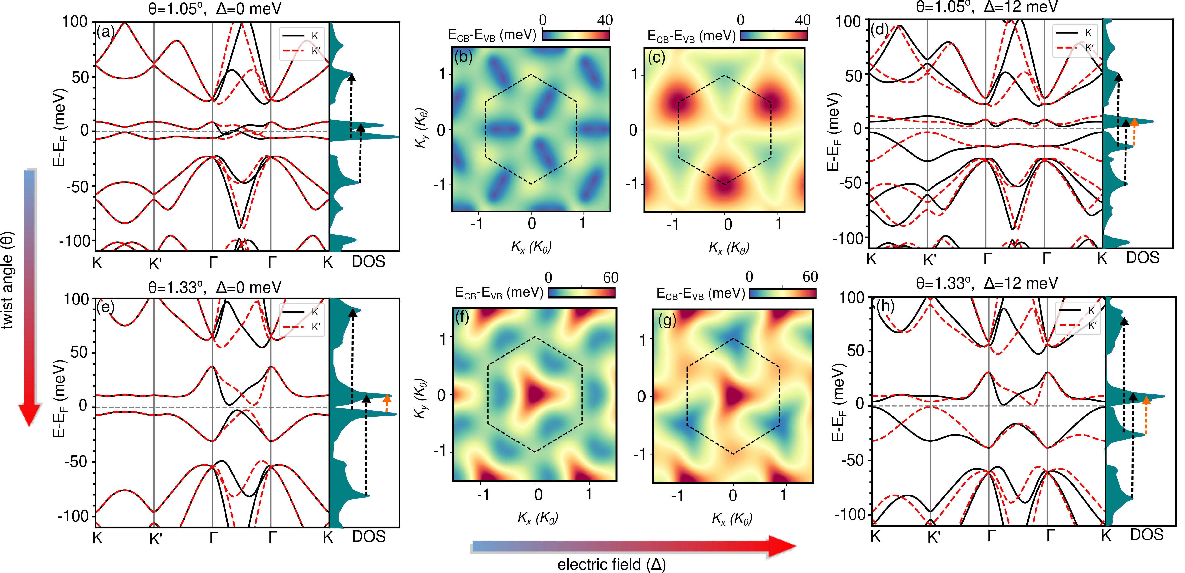
More interestingly, the band dispersion of twisted moiré superlattices, in vicinity of the Fermi energy, are very sensitive to the twist angle (), and to the external electric field () applied perpendicular to the 2D lattice plane. Both these parameters serve as experimental knobs for manipulating the electronic properties of moiré superlattices Choi and Choi (2019); Sinha et al. (2020, 2022); Shen et al. (2020). As an example, we show the evolution of the flat bands of the AB-AB stacked TDBG with the variation of the twist angle and externally applied vertical electric field in Fig. 1. Fig. 1 (a) shows the band dispersion along the high symmetry directions in the Brillouin zone (BZ), together with the DOS at the magic angle, . Similar to the case of TBG, we use the word ‘magic angle’ to imply that the bandwidths of the first conduction and the first valence bands are the smallest possible for this specific angle. Clearly, at the first conduction and first valence bands are almost completely flat (bandwidth within meV range) throughout the whole BZ (see Fig. 1 (b)). The overlapping flat bands induce finite electronic states at the Fermi energy, as reflected in the DOS plot in the right panel of Fig. 1(a). The low energy flat bands are separated from the higher bands with a finite energy gap, referred to as the moiré gap, of value meV. The increment in gradually increases the bandwidth of the flat bands, in addition to inducing a finite energy gap between the two flat bands in vicinity of the CNP [see Fig. 1 (e), (f)]. The band structure and DOS for TDBG at a slightly higher twist angle are presented in Fig. 1 (e). Although the pair of flat bands near the Fermi energy are relatively more dispersing around the point, the flat characteristics of the bands persist over rest of the BZ (see Fig. 1 (f)). This also appears as VHS in the corresponding DOS. The three-fold rotation () symmetry of TDBG is clearly depicted in the direct band gap plots of Fig. 1 (b) and (f). The absence of any zero value in Fig. 1 (f), establishes the insulating nature of the ground state of TDBG with .
Compared to TBG, TDBG offers a higher tunability of its electronic properties with an external electric field. The impact of electric field is introduced in the Hamiltonian via a diagonal potential term () as presented in detail in the Sec. A1 of SI Not (2022). Its impact on electronic properties is represented by the horizontal arrow in Fig. 1. The band dispersion together with DOS of TDBG at and in presence of meV are presented in Fig. 1 (d) and (h), respectively. At the magic angle, the pair of narrow bands at the CNP start to gap out on application of finite electric field beyond a critical threshold. We calculate the critical field required to promote an overall insulating state at the magic angle to be meV. The DOS plot of Fig. 1 (d) shows two distinct VHS around the Fermi energy with a finite gap at the CNP. In contrast to the gapless dispersion at CNP of Fig. 1 (b), the finite gap throughout the BZ in presence of meV makes the system insulating (see Fig. 1 (c)). Similarly, we find that the application of a finite electric field in TDBG with leads to an increased energy separation between the VHS of the flat bands near the CNP in Fig. 1 (h).
Clearly the external perturbations such as twist angle and vertical electric field can mediate the metal insulator transition in TDBG, and can tune the location of the VHS as well. This tunability of the electronic spectrum will also translate into the tunability of the collective charge mode or plasmons in moiré systems with VHS. Before demonstrating this, we explore the fundamental physics of the interband and intraband plasmons in moiré systems.
III Gapped and slow interband plasmons
The combination of electronic flat bands and VHS near the CNP in moiré superlattices motivates several intriguing questions about their plasmon modes. For example, why do the intraband plasmon modes in 2D metallic moiré systems deviate from the characteristic dispersion and become ‘flat’ or non-dispersing? What are the conditions needed for the existence of interband plasmon modes? Is there any connection of the plasmon modes to the VHS in electronic states?
To address such questions, we calculate the plasmon dispersion of TDBG by evaluating the frequency and momentum dependent longitudinal dielectric function . Starting from the single-particle Hamiltonian, , we s compute by numerically evaluating the non-interacting density-density response function (see Sec. A2 of SI Not (2022) for details). The interacting density-density response function is then obtained within the time dependent Hartree approximation or the random phase approximation (RPA) Giuliani and Vignale (2005). Within RPA, the dielectric function is specified by
| (2) |
Here, is Fourier transform of the Coulomb potential in 2D, with and denoting the vacuum permittivity and the static dielectric constant of the background substrate, respectively. The collective charge modes are specified by the zeros of the real part of . In Eq. (2), the noninteracting density-density response function or the ‘Lindhard’ function, , can be expressed as Giuliani and Vignale (2005); Lewandowski and Levitov (2019); Dutta et al. (2022),
| (3) |
The prefactor accounts for the degeneracy of the states, which can arise from the two spin and two valley degrees of freedom Lewandowski and Levitov (2019). The summation runs over the -points of the moiré BZ, the indices , specify the bands and denotes Fermi-Dirac distribution function. describes the band overlap function between the cell periodic part of the Bloch eigenstates at momentum and . See Sec. A2 and Sec. B of the SI Not (2022) for details of the numerical calculation of the dielectric function. Experimentally, plasmon modes are probed via the ‘scattering type near field optical microscopy’ which does the nano-imaging of plasmonic excitations in the real space or through the inelastic ‘electron energy loss spectroscopy’ (EELS) Fei et al. (2012); Dong et al. (2021); Chen et al. (2012); Roth et al. (2014). The plasmon modes appear as peaks in the loss function, , spectrum that is related to the dielectric function via
| (4) |
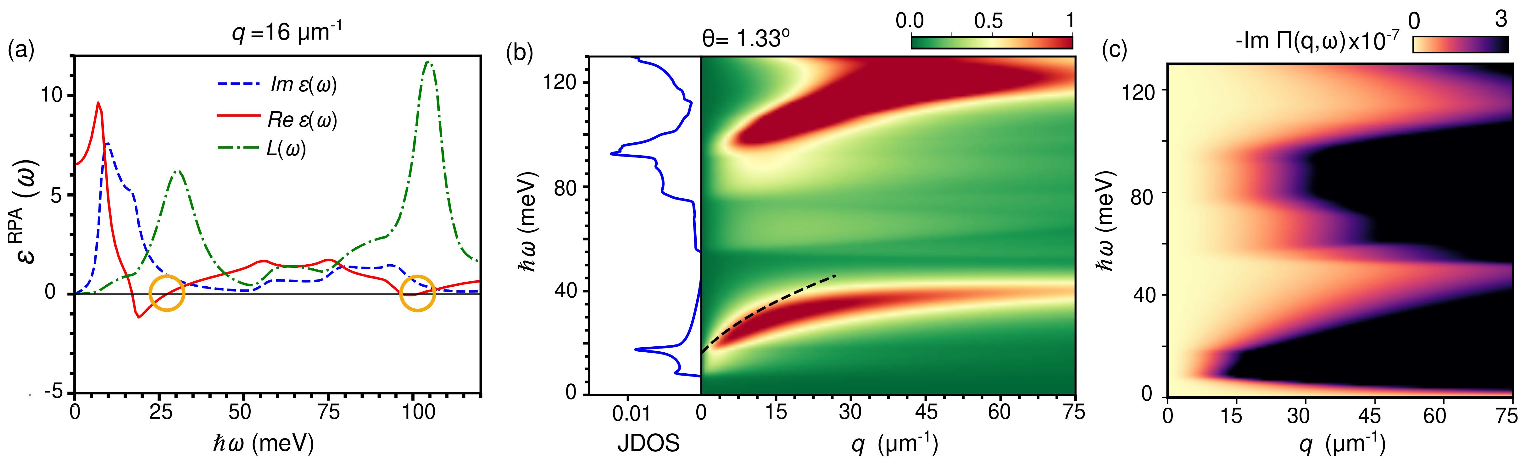
We present the calculated as a function of in Fig. 2(a), for insulating TDBG with . Here, we have chosen the chemical potential to lie in the CNP gap ( meV), and a small value () along the direction. Two distinct zeros in the real part of the dielectric function, marked in orange circles in Fig. 2(a), are located at meV, and meV. Both zeros of the dielectric function are accompanied by peaks in the loss function (green line in Fig. 2 (a)), and have negligible imaginary parts, indicating that these are long lived plasmon modes Agarwal et al. (2014); Agarwal and Vignale (2015). Since there are no free carriers at the Fermi energy (see Fig. 1 (d)), both of these plasmon modes arise solely from interband correlations. To probe the features of these interband plasmon modes, we present the distribution of the loss spectrum in the and (in the direction) plane, along with the calculated JDOS in Fig. 2(b). More interestingly, we find that the plasmon gap at is equal to the energy value corresponding to the peak in the JDOS, shown in the left panel of Fig. 2(b).
Physically, the interband plasmon mode is excited by a time dependent electric field, which initially originates either from internal charge density fluctuations or is applied externally. This dynamical electric field leads to interband transitions predominantly for frequencies corresponding to the JDOS peak simply because of the presence of a large number of transition states. This builds up oscillating charge densities in the system, which further induce a dynamical electric field in the system. This cycle becomes self sustaining in a resonant condition, which manifests as interband plasmon modes.
The intense plasmon modes seen in the distribution of the loss function in Fig. 2(b) clearly show that the interband plasmon modes in TDBG are reasonably long lived. To explicitly confirm that the interband plasmon modes are not Landau damped by electron-hole excitations, we show the boundary of the single particle excitations in Fig. 2(c) via the color plot of the imaginary part of the noninteracting density-density response function Giuliani and Vignale (2005). It is clear from the plot that the interband plasmon modes predominantly lie outside the electron-hole continuum. The plasmon modes comes close to the electron-hole continuum only for . The partial damping of the plasmon mode at sufficiently higher momentum transfer is also corroborated through the loss in the intensity of the loss function spectrum. The next interband plasmon peak in the loss spectrum at meV originates from the VHS in the JDOS arising from the transition between the flat bands and the higher moiré bands of TDBG. The color map of for along the direction also shows similar characteristics, as shown in Sec. C of SI Not (2022). Another interesting feature of the plasmons in moiré superlattices including TDBG, is their extremely ‘flat’ dispersion for large values [see Fig. 2 (b)]. Similar interband plasmons with flat dispersion have also been predicted in small angle TBG Stauber and Kohler (2016); Hesp et al. (2021); Kuang et al. (2021); Novelli et al. (2020). However, the origin of the flat plasmon dispersion at large , is not well understood. In addition, fundamental physics questions related to the origin of the interband plasmon modes and the criterion of their existence are still unanswered. We focus on some of these questions below.
III.1 Origin and dispersion of the interband plasmons
To understand i) the connection of the interband plasmon modes to VHS, and ii) the origin of their flat dispersion, we start from the Lindhard function in Eq. (3). The interband part of the density-density response function can be expressed as Lewandowski and Levitov (2019),
| (5) |
Focusing on the lowest plasmon mode in Fig 2 (b), lets work with the pair of moiré flat bands (, 1st conduction/valance band, labeled as 1/2) near the CNP, and the corresponding VHS peaks in the DOS (see Fig. 1(e)). Using the flat nature of the bands, we can express the energy difference between them as , where is the constant energy difference between the two lowest VHS peaks, and the momentum dependent gap variation is relatively small. For an insightful, but approximate estimation of the plasmon dispersion, we neglect the term in the Lindhard function. In fact, this approximation should also work in other systems without flat bands, as the VHS points in the JDOS carry the maximum contribution in the BZ momentum sum in Eq. (5).
With this simplification, the dispersion of the lowest interband plasmons mode for the insulating moiré systems, can now be obtained from . For 2D systems, this yields
| (6) |
where we have defined,
| (7) |
This gives the interband plasmon dispersion in 2D to be,
| (8) |
This analytical model for the dispersion of the interband plasmon mode is one of the most important results of this work. Eq. (8) establishes the following two criterion (necessary condition) for the existence of interband plasmon modes: i) the presence of a VHS peak in the electronic JDOS, and ii) the interband correlation being finite for those pair of bands which contribute dominantly to the JDOS peak. In fact, the gap of the plasmon mode is specified by the energy of the JDOS peak, while the interband correlations determine its dispersion.
III.2 Gapped interband plasmons in the limit
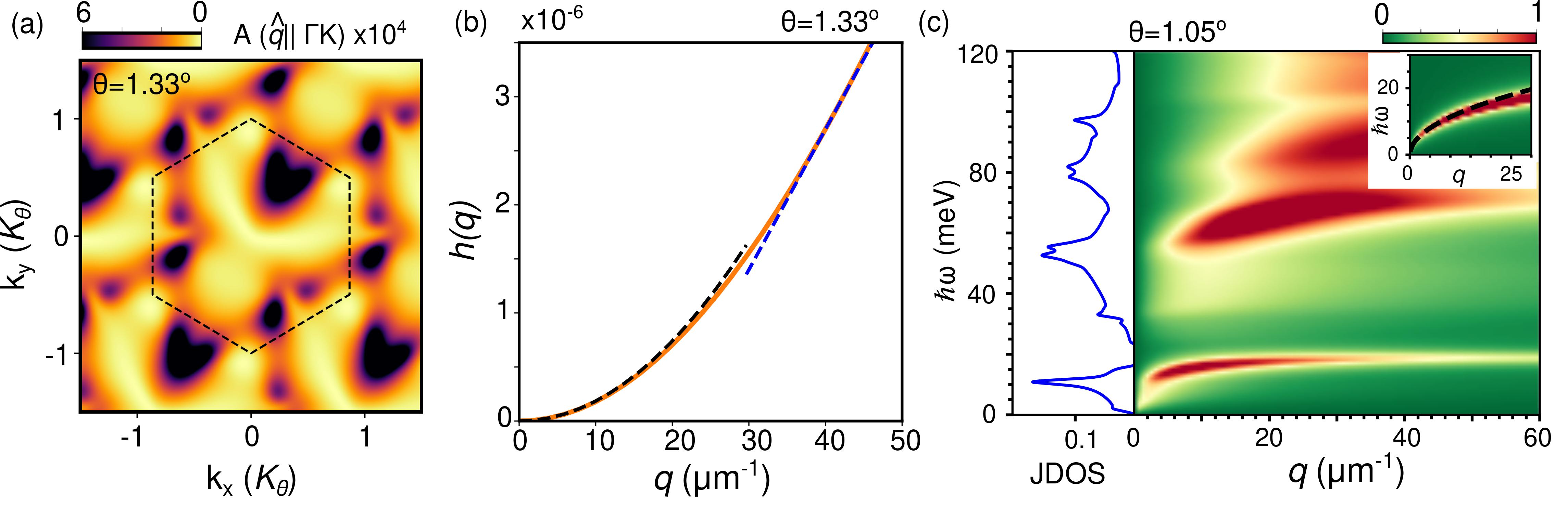
In the long wavelength () limit, we have , where, depends on the direction of and the interband Berry connection, of the pair of bands involved. The distribution of over the 2D BZ for momentum transfer along the direction is presented in Fig. 3(a) for . This gives a universal analytical form for the long wavelength interband plasmon dispersion,
| (9) |
This highlights i) the universal nature of the 2D interband plasmon dispersion in the long wavelength limit, and ii) the interband plasmon mode exists only in presence of a finite interband Berry connection for those pair of bands that contribute dominantly to the JDOS peak. We have calculated Eq. (9) for the pair of flat bands near CNP (16 meV) at , and shown in Fig. 2 (b) to compare with the numerically calculated lowest interband plasmon dispersion. From the quadratic fit of , we estimate , given in as shown in Fig. 3 (b). Furthermore, we have also checked Eq. (9) for two other examples of graphene, and in a toy model for bilayer graphene with a large effective mass, which also supports interband plasmons (see Sec. E and Sec. F of the SI Not (2022) for details). The small expansion of Eq. (9) reduces to a linear dispersion very close to the origin [see Fig. 2 (b)] Hesp et al. (2021); Zhang et al. (2017). Therefore, the observation of interband plasmon highlights the existence of a finite interband Berry connection for those pair of bands which contribute dominantly to the JDOS peak.
III.3 Flat interband plasmons in the large limit
In contrast to the universal nature of the long wavelength interband plasmon dispersion, the large limit of the interband plasmon dispersion is determined by the non-universal factor in Eq. (8). This nonuniversal factor gives rise to the flat interband plasmon dispersion in moiré superlattices. The numerically calculated , for the two flat bands in an insulating TDBG from the continuum Hamiltonian, is shown in Fig. 3 (b) for along the direction. For small values, the numerical curve follows the quadratic relation as shown by black dashed line. More interestingly, Fig. 3(b) clearly shows that for , the curve starts to deviate from the behavior. In fact, we find that for , it becomes linear (indicated by the blue dashed line). In this linear regime, the term in Eq. (8) becomes independent of , making the interband plasmon nondispersive or flat. Owing to the very small group velocity, these flat plasmons are also referred to as ‘slow’ plasmons da Jornada et al. (2020).
To highlight that the interband plasmon modes need not always have a flat dispersion, we explicitly calculate the interband plasmon dispersion of the monolayer graphene and bilayer graphene model with a large effective mass, in Sec. E and Sec. F of the SI Not (2022), respectively. In both cases, we find that the interband plasmon mode indeed begins from the energy of the VHS in the JDOS. However, we find that, in contrast to being flat in the large limit, the interband plasmon mode disperses linearly in the monolayer graphene and massive bilayer graphene model. This reaffirms the nonuniversal and material dependent aspect of the large limit of the interband plasmon mode.
IV Flat intraband plasmon in metallic moiré systems
In addition to the interband plasmons arising from interband correlations, metallic moire systems also host an intraband plasmon mode arising from density fluctuations around the Fermi surface. The long wavelength (or ) limit of the intraband plasmon dispersion can be computed from charge stiffness or Drude weight () Novelli et al. (2020); Sachdeva et al. (2015), and it is given by
| (10) |
The undoped TDBG shows metallic behavior at the CNP for the magic angle [see Fig. 1 (a)]. We present the color plot of the loss function for TDBG in Fig. 3 (c). The inset shows only the intraband contribution to the loss function, with the black dashed line representing the intraband plasmon dispersion relation of Eq. (10). The Drude weight is numerically calculated to be 13.5 meV in scale of (see Sec. B of the SI Not (2022) for details). This intraband mode is also outside the electron-hole continuum and is long lived, as shown in SI Not (2022). Clearly, the low energy intraband plasmon dispersion in TDBG deviates significantly from expected behavior as shown in Fig. 3(c). Similarly to the case of the interband plasmon mode, with increasing , the intraband plasmon dispersion in TDBG also becomes flat and nondispersive, giving rise to slow plasmons. This can be clearly seen in Fig. 3 (c), where the intraband plasmon dispersion in the energy window - meV becomes flat in large limit. This is primarily an influence of the strong interband correlations of the flat bands, which have a JDOS peak at meV [see Fig. 3 (c)], which drastically modifies the intraband plasmon dispersion.
To understand the (i) nature of the intraband plasmon dispersion under the influence of large interband transitions, and (ii) the flatness of the dispersion at large , we express the Lindhard function as the sum of two different contributions, Lewandowski and Levitov (2019). These contributions are separated depending on the energy difference = being smaller or larger than . For example, at the magic angle, the TDBG band dispersion has a gap between the flat bands and the higher energy moiré bands. Therefore, to explore the dispersion of the intraband mode, the flat band contribution should be retained in the first term, while the contribution of the higher bands will go in the second term. In the () term, we have () in the denominator of Eq. (3), and we approximate,
| (11a) | |||||
| (11b) | |||||
Here, the summation () runs over the pair of bands such that the eigenvalues satisfy (). This allows us to express the dielectric function as
| (12) |
where we have defined and . Now, the overall plasmon dispersion can be obtained from the roots of the dielectric function to be,
| (13) |
which is valid for both small and large limit. In the small limit, the intraband band overlap function dominates compared to the interband overlap function (see Eq. S19 of SI. Not (2022)). Therefore, term in the denominator have vanishingly small contribution in low limit. So, the plasmon dispersion is predominantly dictated by (intraband contributions only) and we have [see Sec. D of the SI Not (2022) for details]. This establishes that, in the long wavelength limit, the intraband plasmon mode in 2D moire systems also disperses as .
In the large limit, comparable to the half of the moire reciprocal lattice vectors, the contribution of becomes large compared to unity, and it starts influencing the plasmon dispersion. Consequently, the dispersion of the plasmons is modified to Lewandowski and Levitov (2019). The ratio becomes nearly independent of for large in TDBG, and this is what modifies the dispersion to become nearly independent flat dispersion, supporting very slow plasmons. This clearly highlights the role of strong interband transitions [term ] in modifying the intraband plasmon dispersion in the large limit.
Having established the universal and the non-universal features of both the intraband and the interband plasmon mode, we now study their tunability.
V Tunability of the plasmon modes in TDBG
One of the experimental advantages of TDBG is the relatively large tunability of the electronic band dispersion as highlighted in Fig. 1. In this section we demonstrate that the vertical electric field, the twist angle and electronic doping can also be used as knobs to modulate the interband and intraband plasmon dispersion in TDBG. Experimentally, electrostatic gating via a combination of the top and the back gate can be used to apply a vertical electric field and to change the electron doping in a controlled way Sinha et al. (2020, 2022).
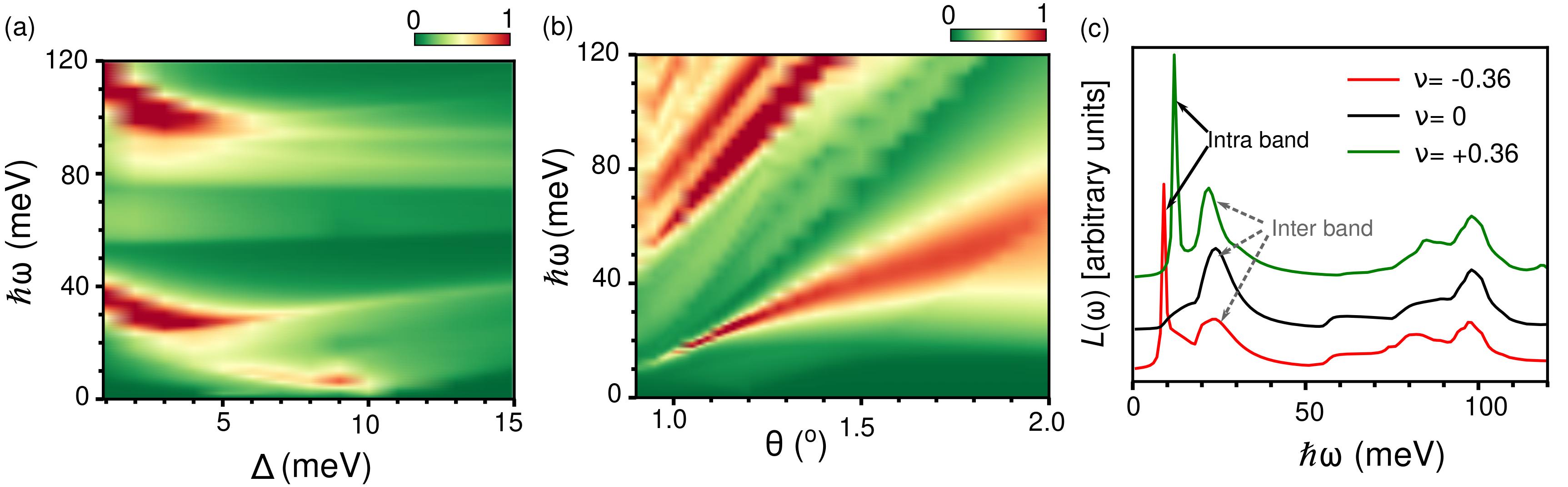
The impact of the vertical electric field on the low energy plasmon modes of small angle TDBG is shown in Fig. 4 (a), for . With increasing electric field strength, the plasmon peaks in Fig. 4 (a) trace the evolution of the JDOS peaks and mark the metal insulator transition. For , the plasmon mode at meV originates from the interband transitions between the two flat bands, whereas the correlations between the flat bands and the moiré bands give rise to the plasmon mode around meV. On initially increasing the electric field, the band gap and the location of the VHS first decreases upto meV. This is reflected in the loss function spectrum as a red shift of the plasmon mode. As , the flat bands touch each other at the high symmetry / points [see Fig. S7 (c) in the SI Not (2022)] giving rise to a metallic state. The transition to the metallic state is reflected in Fig. 4(a) as an extra peak (around meV) for an intraband plasmon mode. Further increment in meV opens up a gap in the electronic spectrum, and consequently the intraband plasmon mode vanishes. With gradual enhancement of the electric field, the bands become more dispersive, and the VHS peak in the JDOS decreases in strength. This is well captured by the loss function spectrum and is reflected in the diminishing weight of the interband plasmon peaks for meV. This clearly establishes that the loss function spectrum can also be used to probe the metal insulator transition and the evolution of the JDOS peaks in TDBG and in other moiré systems as well. More interestingly, experimentally accessible electric field values can tune the plasmon frequencies by more than 30%.
The variation of the plasmon dispersion on changing the twist angle is captured in Fig. 4 (b). We find that the ladder of plasmon modes in TDBG persists for a wide range of twist angles. TDBG is metallic up to with relatively flat bands that give rise to VHS in the DOS. This is reflected in the sharp low energy intraband plasmon peak for small angle TDBG. When the twist angle becomes larger than a critical value (), the system becomes insulating, and the sharp intraband plasmon mode evolves into a more dispersive and relatively less intense interband plasmon mode arising from transitions between the flat bands. In addition to this, the energy separation between the bands, and consequently the location of the VHS increases linearly with increasing twist angle. This is also captured by the loss function in Fig. 4(b) as the energy of all the interband plasmon modes simply traces the location of the VHS in the JDOS.
Another control parameter for tuning the low energy plasmon modes in TDBG and other moiré systems is the electron doping (). For example, by tuning the chemical potential to lie within the CNP gap or within the moiré gap, we can eliminate the intraband plasmon mode. We show this explicitly in the plot for three different electron doping values ( and 0) in Fig. 4 (c). At in Fig. 4 (c), there are only interband plasmon peaks at and meV, arising from the VHS in the JDOS for interband transitions. Tuning the chemical potential to be in either the conduction () or in the valence () band, gives rise to an additional intraband plasmon peak in the loss function spectrum, whose dispersion and intensity can be further tuned by varying the electron doping.
VI Discussion
We have demonstrated that small angle TDBG hosts several long lived and slow plasmon modes with a flat dispersion in an energy window of 0-100 meV. We showed that the necessary criteria for the existence of the interband plasmon modes are i) the presence of a VHS in the JDOS, and ii) a finite interband Berry connection between the pair of bands giving rise to the VHS. We find that each of these interband plasmons has a universal gapped dispersion of the form in the long wavelength limit, where marks the location of the VHS in the JDOS, and is a material specific parameter. In addition to the interband plasmon modes, metallic TDBG also supports a gapless intraband plasmon mode, which disperses as as . The intraband as well as the interband plasmon modes have a nonuniversal dispersion in the large limit, which becomes flat in moiré superlattices.
We have demonstrated that the long lived and flat plasmon modes in TDBG are highly tunable and they can be controlled by the vertical electric field, electron doping and they persist over a wide range twist angle. We have shown that the change of the interband plasmon peak with the twist angle or vertical electric field captures the separation of the flat and moiré bands or the VHS in the JDOS. The low energy, flat, long lived and tunable terahertz plasmon modes in TDBG offers a unique platform for studying the fundamental aspects and potential application of photon based quantum information processing.
Acknowledgment
A.C acknowledges Indian Institute of Technology, Kanpur and Science and Engineering Research Board (SERB) National Postdoctoral Fellowship (PDF/2021/000346), India for funding. We thank Mandar M. Deshmukh and Barun Ghosh for useful comments. We acknowledge the Science and Engineering Research Board (SERB) and the Department of Science and Technology (DST) of the Government of India for financial support. We thank CC-IITK for providing the high performance computing facility.
References
- Pines and Bohm (1952) D. Pines and D. Bohm, Physical Review 85, 338 (1952).
- Pines and Schrieffer (1962) D. Pines and J. R. Schrieffer, Physical Review 125, 804 (1962).
- Pines and Noziéres (1966) D. Pines and Noziéres, The Theory of Quantum Liquids (1st ed.) (CRC Press, 1966).
- Alonso Calafell et al. (2019) I. Alonso Calafell, J. D. Cox, M. Radonjić, J. R. M. Saavedra, F. J. García de Abajo, L. A. Rozema, and P. Walther, npj Quantum Information 5, 37 (2019).
- Tame et al. (2013) M. S. Tame, K. R. McEnery, Ş. K. Özdemir, J. Lee, S. A. Maier, and M. S. Kim, Nature Physics 9, 329 (2013).
- Wang et al. (2021) J. Wang, X. Sui, W. Duan, F. Liu, and B. Huang, Proceedings of the National Academy of Sciences 118, e2023029118 (2021).
- Politano et al. (2018) A. Politano, G. Chiarello, B. Ghosh, K. Sadhukhan, C.-N. Kuo, C. S. Lue, V. Pellegrini, and A. Agarwal, Phys. Rev. Lett. 121, 086804 (2018).
- Rivera and Kaminer (2020) N. Rivera and I. Kaminer, Nature Reviews Physics 2, 538 (2020).
- Gullans et al. (2013) M. Gullans, D. E. Chang, F. H. L. Koppens, F. J. G. de Abajo, and M. D. Lukin, Phys. Rev. Lett. 111, 247401 (2013).
- Song and Rudner (2016) J. C. W. Song and M. S. Rudner, Proceedings of the National Academy of Sciences 113, 4658 (2016).
- Sadhukhan et al. (2020) K. Sadhukhan, A. Politano, and A. Agarwal, Phys. Rev. Lett. 124, 046803 (2020).
- Yu et al. (2019) H. Yu, Y. Peng, Y. Yang, and Z.-Y. Li, npj Computational Materials 5, 45 (2019).
- Yan et al. (2013) H. Yan, T. Low, W. Zhu, Y. Wu, M. Freitag, X. Li, F. Guinea, P. Avouris, and F. Xia, Nature Photonics 7, 394 (2013).
- Andress et al. (2012) W. F. Andress, H. Yoon, K. Y. M. Yeung, L. Qin, K. West, L. Pfeiffer, and D. Ham, Nano Letters 12, 2272 (2012).
- Agarwal et al. (2014) A. Agarwal, M. Polini, G. Vignale, and M. E. Flatté, Phys. Rev. B 90, 155409 (2014).
- Agarwal et al. (2018) A. Agarwal, M. S. Vitiello, L. Viti, A. Cupolillo, and A. Politano, Nanoscale 10, 8938 (2018).
- Liang et al. (2021) G. Liang, X. Yu, X. Hu, B. Qiang, C. Wang, and Q. J. Wang, Materials Today 51, 294 (2021).
- Woessner et al. (2015) A. Woessner, M. B. Lundeberg, Y. Gao, A. Principi, P. Alonso-González, M. Carrega, K. Watanabe, T. Taniguchi, G. Vignale, M. Polini, J. Hone, R. Hillenbrand, and F. H. L. Koppens, Nature Materials 14, 421 (2015).
- Gao et al. (2012) W. Gao, J. Shu, C. Qiu, and Q. Xu, ACS Nano 6, 7806 (2012).
- Zhou et al. (2012) W. Zhou, J. Lee, J. Nanda, S. T. Pantelides, S. J. Pennycook, and J. C. Idrobo, Nature nanotechnology 7, 161 (2012).
- Jablan et al. (2009) M. Jablan, H. Buljan, and M. Soljačić, Physical Review B 80, 245435 (2009).
- Fei et al. (2012) Z. Fei, A. S. Rodin, G. O. Andreev, W. Bao, A. S. McLeod, M. Wagner, L. M. Zhang, Z. Zhao, M. Thiemens, G. Dominguez, M. M. Fogler, A. H. C. Neto, C. N. Lau, F. Keilmann, and D. N. Basov, Nature 487, 82 (2012).
- Sachdeva et al. (2015) R. Sachdeva, A. Thakur, G. Vignale, and A. Agarwal, Phys. Rev. B 91, 205426 (2015).
- Hwang and Das Sarma (2007) E. H. Hwang and S. Das Sarma, Physical Review B 75, 205418 (2007).
- Kinyanjui et al. (2012) M. K. Kinyanjui, C. Kramberger, T. Pichler, J. C. Meyer, P. Wachsmuth, G. Benner, and U. Kaiser, Euro Physics Letters 97, 57005 (2012).
- Despoja et al. (2013) V. Despoja, D. Novko, K. Dekanić, M. Šunjić, and L. Marušić, Phys. Rev. B 87, 075447 (2013).
- Politano and Chiarello (2014) A. Politano and G. Chiarello, Nanoscale 6, 10927 (2014).
- Ni et al. (2015) G. X. Ni, H. Wang, J. S. Wu, Z. Fei, M. D. Goldflam, F. Keilmann, B. Özyilmaz, A. H. Castro Neto, X. M. Xie, M. M. Fogler, and D. N. Basov, Nature Materials 14, 1217 (2015).
- Wang et al. (2020) J. Wang, W. Bo, Y. Ding, X. Wang, and X. Mu, Materials Today Physics 14, 100238 (2020).
- Bistritzer and MacDonald (2011) R. Bistritzer and A. H. MacDonald, Proceedings of the National Academy of Sciences 108, 12233 (2011).
- Fu et al. (2020) Y. Fu, E. J. König, J. H. Wilson, Y.-Z. Chou, and J. H. Pixley, npj Quantum Materials 5, 71 (2020).
- Haddadi et al. (2020) F. Haddadi, Q. Wu, A. J. Kruchkov, and O. V. Yazyev, Nano Letters 20, 2410 (2020).
- Burg et al. (2019) G. W. Burg, J. Zhu, T. Taniguchi, K. Watanabe, A. H. MacDonald, and E. Tutuc, Physical Review Letters 123, 197702 (2019).
- Andrei and MacDonald (2020a) E. Y. Andrei and A. H. MacDonald, Nature Materials 19, 1265 (2020a).
- Shen et al. (2020) C. Shen, Y. Chu, Q. Wu, N. Li, S. Wang, Y. Zhao, J. Tang, J. Liu, J. Tian, K. Watanabe, T. Taniguchi, R. Yang, Z. Y. Meng, D. Shi, O. V. Yazyev, and G. Zhang, Nature Physics 16, 520 (2020).
- Cao et al. (2020) Y. Cao, D. Rodan-Legrain, O. Rubies-Bigorda, J. M. Park, K. Watanabe, T. Taniguchi, and P. Jarillo-Herrero, Nature 583, 215 (2020).
- Sinha et al. (2022) S. Sinha, P. C. Adak, A. Chakraborty, K. Das, K. Debnath, L. D. V. Sangani, K. Watanabe, T. Taniguchi, U. V. Waghmare, A. Agarwal, and M. M. Deshmukh, “Berry curvature dipole senses topological transition in a moiré superlattice; arxiv:10.48550/arxiv.2204.02848,” (2022).
- Cea and Guinea (2021) T. Cea and F. Guinea, Proceedings of the National Academy of Sciences 118, e2107874118 (2021).
- Liu and Dai (2020) J. Liu and X. Dai, npj Computational Materials 6, 57 (2020).
- Bennett and Remez (2022) D. Bennett and B. Remez, npj 2D Materials and Applications 6, 7 (2022).
- Novelli et al. (2020) P. Novelli, I. Torre, F. H. L. Koppens, F. Taddei, and M. Polini, Physical Review B 102, 125403 (2020).
- Stauber and Kohler (2016) T. Stauber and H. Kohler, Nano Letters 16, 6844 (2016).
- Lewandowski and Levitov (2019) C. Lewandowski and L. Levitov, Proceedings of the National Academy of Sciences 116, 20869 (2019).
- Kuang et al. (2021) X. Kuang, Z. Zhan, and S. Yuan, Physical Review B 103, 115431 (2021).
- Hesp et al. (2021) N. C. H. Hesp, I. Torre, D. Rodan-Legrain, P. Novelli, Y. Cao, S. Carr, S. Fang, P. Stepanov, D. Barcons-Ruiz, H. Herzig Sheinfux, K. Watanabe, T. Taniguchi, D. K. Efetov, E. Kaxiras, P. Jarillo-Herrero, M. Polini, and F. H. L. Koppens, Nature Physics 17, 1162 (2021).
- Sharma et al. (2020) G. Sharma, M. Trushin, O. P. Sushkov, G. Vignale, and S. Adam, Physical Review Research 2, 022040 (2020).
- Lewandowski et al. (2021) C. Lewandowski, D. Chowdhury, and J. Ruhman, Physical Review B 103, 235401 (2021).
- Andrei and MacDonald (2020b) E. Y. Andrei and A. H. MacDonald, Nature Materials 19, 1265 (2020b).
- Not (2022) Supplementary Information: It has more details on, i) the continuum model for TDBG, ii) efficient computation of the dielectric function, iii) optical conductivity of TDBG, iv) direction dependence of the plasmon dispersion, its long wavelength limit, its tunability and v) interband plasmon mode in graphene, and in massive bilayer graphene (2022).
- Choi and Choi (2019) Y. W. Choi and H. J. Choi, Physical Review B 100, 201402 (2019).
- Sinha et al. (2020) S. Sinha, P. C. Adak, R. S. Surya Kanthi, B. L. Chittari, L. D. V. Sangani, K. Watanabe, T. Taniguchi, J. Jung, and M. M. Deshmukh, Nature Communications 11, 5548 (2020).
- Giuliani and Vignale (2005) G. Giuliani and G. Vignale, Quantum Theory of the Electron Liquid (Cambridge University Press, 2005).
- Dutta et al. (2022) D. Dutta, B. Ghosh, B. Singh, H. Lin, A. Politano, A. Bansil, and A. Agarwal, Phys. Rev. B 105, 165104 (2022).
- Dong et al. (2021) Y. Dong, L. Xiong, I. Y. Phinney, Z. Sun, R. Jing, A. S. McLeod, S. Zhang, S. Liu, F. L. Ruta, H. Gao, Z. Dong, R. Pan, J. H. Edgar, P. Jarillo-Herrero, L. S. Levitov, A. J. Millis, M. M. Fogler, D. A. Bandurin, and D. N. Basov, Nature 594, 513 (2021).
- Chen et al. (2012) J. Chen, M. Badioli, P. Alonso-González, S. Thongrattanasiri, F. Huth, J. Osmond, M. Spasenović, A. Centeno, A. Pesquera, P. Godignon, A. Zurutuza Elorza, N. Camara, F. J. G. de Abajo, R. Hillenbrand, and F. H. L. Koppens, Nature 487, 77 (2012).
- Roth et al. (2014) F. Roth, A. König, J. Fink, B. Büchner, and M. Knupfer, Journal of Electron Spectroscopy and Related Phenomena 195, 85 (2014).
- Agarwal and Vignale (2015) A. Agarwal and G. Vignale, Phys. Rev. B 91, 245407 (2015).
- Zhang et al. (2017) F. Zhang, J. Zhou, D. Xiao, and Y. Yao, Physical Review Letters 119, 266804 (2017).
- da Jornada et al. (2020) F. H. da Jornada, L. Xian, A. Rubio, and S. G. Louie, Nature Communications 11, 1013 (2020).